DESIGN, FABRICATION AND RF
CHARACTERIZATION OF KA-BAND
SILICON IMPATT DIODE
TAPAS KUMAR PAL
Research Centre Imarat Vignyana Kancha Hyderabad – 500 069, INDIA.
J. P. BANERJEE
Centre for Millimeterwave Semiconductor Devices and Systems Institute of Radiophysics and Electronics
University of Calcutta, Kolkata – 700009, INDIA.
Abstract:
A silicon (p+nn+) SDR IMPATT diode for Ka-band operation has been designed by using a double iterative DC and Small signal simulation which involves simultaneous solution of Poisson’s equation and Carrier continuity equation, satisfying appropriate boundary conditions in the depletion layer edges. Using the design parameters, silicon epitaxial n/n+ wafers of appropriate thickness and resistivity of the epitaxial layer have been selected for fabrication of (p+nn+) SDR IMPATT diode for Ka-band operation. The (p+nn+) SDR IMPATT diode has been fabricated through diffusion technique. The optimized process steps of fabrication, starting from wafer cleaning to packaging have been described in details. The DC V-I and RF characteristics of fabricated IMPATT diode have been measured by using an integrated heat sink cum resonant cap waveguide cavity.
Keywords: Design, Fabrication, RF characterization, Small signal simulation, Silicon SDR IMPATT diode.
1. Introduction
IMPact Avalanche Transit Time (IMPATT) devices have emerged as most powerful solid-state devices for generation of high CW and pulsed power at millimeter wave frequencies [1], [2]. These devices provide high oscillator output power with high DC to RF conversion efficiency in Silicon Monolithic Millimeter Wave Integrated Circuits (SIMMWIC) [3]. The authors have designed a silicon (p+nn+) SDR IMPATT diode for Ka-band operation by using double iterative DC and Small signal simulation methods which involve simultaneous solution of Poisson’s and Carrier continuity equation with appropriate boundary conditions at the depletion layer edges [4]. Based on the DC and Small Signal simulation the authors have appropriately selected silicon epitaxial wafers with phosphorus and antimony as n and n+ dopants respectively. The substrate resistivity is selected in the range of 0.0174 - 0.0185 ohm-cm and epitaxial resistivity in the range of 0.45-0.55 ohm-cm [5] for fabrication of (p+nn+) SDR Ka- band IMPATT Diode.
The metallurgical junction of a silicon (p+nn+) SDR IMPATT diode can be grown by different techniques i.e. (i). Diffusion (ii). Ion implantation (iii). Chemical vapor deposition and ( iv). Molecular Beam Epitaxy (MBE) . The authors have chosen the diffusion route since it is the simplest method of fabrication of single drift diode, which involves diffusion of p-type impurities in n/n+ epitaxial wafer [6]. The authors have used Boron as p-type dopant since it can be diffused into silicon by solid source like Boron Nitride (BN), liquid source like Boron Tri Bromide (BBr3) and gaseous source like Diborane (B2H6). The source BBr3 is highly volatile in nature and B2H6 is highly toxic, therefore solid source BN is chosen for easy handling of the doping source.
For DC and RF characterization the diode is to be placed in a suitable microwave/mm wave cavity and mm wave power is delivered by the device biased to break down [7]. The authors have used a resonant cap wave guide mount [8] consisting of a resonant cap structure under which the diode is embedded and the two together are mounted in a rectangular wave guide. The cap and the bottom surface of the wave guide form a localized radial cavity around the diode. The mm wave signal generated by the diode is coupled to the main rectangular wave guide cavity through the vertical open edges of the radial cavity.
2. DC and Small Signal Simulation
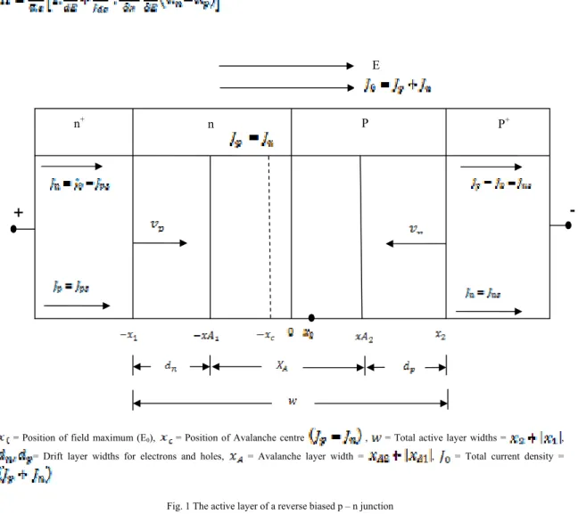
One-dimensional model of a reverse biased junction diode considered by the authors for DC and Small signal simulation has been schematically shown in Fig.1, with symbols having their usual meaning [9]. The total current is composed of conduction current and displacement current only because the diffusion current is negligibly small. The total current density is thus given by
(1)
The spatial variation of electric field in the space charge layer is obtained from Poisson’s equation as
(2)
Where E = electric field, q = electronic charge, = ionized donor density, = ionized acceptor density, p = hole density, n = electron density, = permittivity of the semiconductor.
The equations of continuity for electrons and holes are given by
(3.a)
(3.b)
where g is the generation rate, is the ionization rate and is the velocity of charge carriers. The above mentioned parameters are expressed in the following equations
(3.c)
(3.d)
(3.e)
where indicates the saturated drift velocity and
n,p is the mobility of charge carriers.From the above equations the fundamental time and space dependent differential equation involving the electric field and the total current density under dynamic condition is given by
(4)
= Position of field maximum (E0), = Position of Avalanche centre , = Total active layer widths = ,
= Drift layer widths for electrons and holes, = Avalanche layer width = , = Total current density =
Fig. 1 The active layer of a reverse biased p – n junction
To linearize the non-linear Eq. (4), we introduce a parameter H [10] mentioned above. Hence
(5)
where = ac impedance.
Let the boundaries of regions be at the co-ordinates and respectively. Thus from
Eq. (1), the boundary condition at ( .
(6a)
(6b) from these two equations
E
P P+
n+
n
at the left edge at (n region)
(6d)
Considering and separating the real and imaginary parts, the following second order differential equations are obtained.
(7)
(8)
The boundary conditions are, at
(9a)
(9b)
Similarly at
(9c)
(9d)
The device negative resistance and reactance are obtained from the following
and
Conductance G = (10.a)
Susceptance B (10.b)
Quality factor (11)
3. Design of Ka-band SDR IMPATT Diode
4. Fabrication of SDR IMPATT Diode
Based on the DC and Small signal simulation described in the previous section, the authors have selected the silicon epitaxial n/n+ wafers having the following specification [5] for fabrication of a (p+nn+)SDR Ka- band IMPATT Diode through diffusion route . Fig.6 shows schematic diagram of a silicon epitaxial n/n+ wafer. The optimized process steps followed by the authors are described in details in the following section.
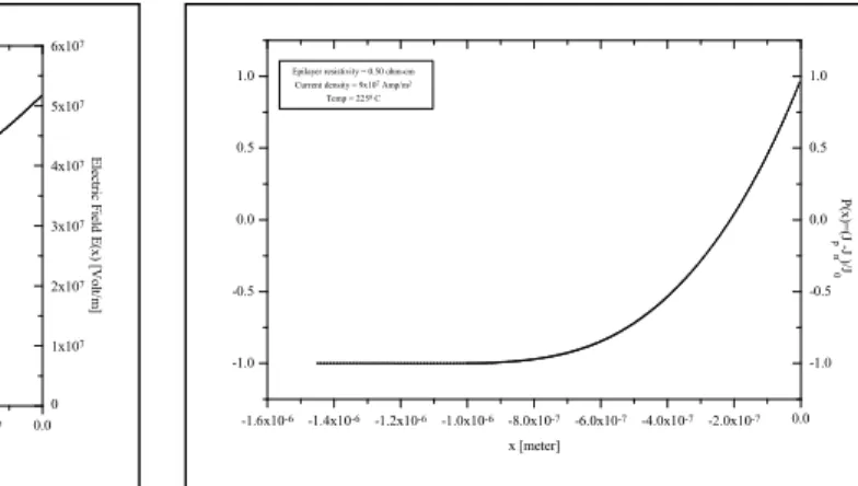
-1.6x10⁻⁶ -1.4x10⁻⁶ -1.2x10⁻⁶ -1.0x10⁻⁶ -8.0x10⁻⁷ -6.0x10⁻⁷ -4.0x10⁻⁷ -2.0x10⁻⁷ 0.0 0 1x10⁷ 2x10⁷ 3x10⁷ 4x10⁷ 5x10⁷ 6x10⁷ Epilayer resistivity = 0.50 ohm-cm
Current density = 9x10⁷ Amp/m2
Temp = 2250 C
E lec tri c F ield E (x) [ V o lt/m ] x [meter]
-1.6x10⁻⁶ -1.4x10⁻⁶ -1.2x10⁻⁶ -1.0x10⁻⁶ -8.0x10⁻⁷ -6.0x10⁻⁷ -4.0x10⁻⁷ -2.0x10⁻⁷ 0.0 -1.0 -0.5 0.0 0.5 1.0 -1.0 -0.5 0.0 0.5 1.0
Epilayer resistivity = 0.50 ohm-cm
Current density = 9x10⁷ Amp/m2
Temp = 2250 C
P( x )= (J p-J n)/ J 0 x [meter]
-1.6x10⁻⁶-1.4x10⁻⁶-1.2x10⁻⁶-1.0x10⁻⁶-8.0x10⁻⁷-6.0x10⁻⁷-4.0x10⁻⁷-2.0x10⁻⁷ 0.0 2.0x10⁻⁷
1.0x10²²
1.5x10²²
2.0x10²²
2.5x10²²
3.0x10²²
Epilayer resistivity = 0.50 ohm-cm
Current density = 9x10⁷ Amp/m2
Temp = 2250 C
D oping de nsi ty [m 3] x [meter]
-4.5 -4.0 -3.5 -3.0 -2.5 -2.0 -1.5 -1.0
0 5 10 15 20
Epilayer resistivity = 0.50 ohm-cm
Current density = 9x10⁷ Amp/m2
Temp = 2250 C
42 GHz 40 GHz 38 GHz 37 GHz 36.5 GHz 36 GHz 35 GHz 34 GHz 32 GHz 30 GHz 28 GHz 26.5 GHz S u sc ep ta n ce( B) x1 0
6 in
m
h
o
/m
2
Conductance(G)x106 in mho/m2
Fig. 2. Electric field E(x) profiles of silicon SDR (p+
nn+
) IMPATT Diode
Fig. 3. P(x) profiles of silicon SDR (p+
nn+
) IMPATT Diode
Fig. 4. Doping profiles of silicon SDR (p+nn+) IMPATT Diode
Fig. 5. Conductance – Susceptance Plot of silicon SDR (p+
nn+
) IMPATT Diode
Wafer Characteristics:
Type /dopant : N/Phosphorus Wafer Diameter : 7.57 - 7.67 cm Substrate Thickness : 381 25 (micron) Substrate Resistivity : 0.0174 - 0.0185 (ohm-cm) Crystal orientation : <111>
Epitaxial Thickness : 3.6-4.4 micron Epitaxial Resistivity : 0.45-0.55 ohm-cm
4.1 Wafer cleaning
Wafer cleaning is a very important step in mm wave device fabrication process because of the variety of organic and inorganic contaminants of unknown origin, which are present on the semiconductor surface, which deteriorate the performance of the device [13].
a) Wafer is kept in a clean beaker containing DI water having 18 MΩ resistivity which is then placed inside an ultrasonic cleaner for 2- 4 minutes. This cleaning removes contaminating additives from the wafer surface through acoustic streaming [14-15].
b) The wafer is then transferred to a beaker containing hot (80-850C) trichloro-ethelyene (TCE) for 10 to 15 minutes to remove the organic particles like air born bacteria, grease and wax from the surface of the wafer. c) Trichloro - ethelyene (TCE) is removed by acetone.
d) The wafer is then rinsed thoroughly by running in DI water to remove acetone.
e) The wafer is then transferred to a beaker containing solution of NH4OH : H2O2 : H2O in ratio of 10:20:70 and heated to 80-850C for 10 to 15 minutes to remove heavy metallic impurities [16].
f) The wafer is rinsed with running DI water.
g) The wafer is immersed in a beaker containing solution of HCL: H2O2 : H2O in the ratio of 10:20:70 and heated to 80-850C for 10-15 minutes to remove light metallic impurities.
h) It is then rinsed thoroughly in running DI water.
i) To make the mirror like hydrophobic surface, the wafer is dipped into a solution containing H2O : HF :: 90:10 for 1-2 minutes.
j) The wafer is finally rinsed by running DI water. Then N2 gas blower is used to dry up the wafer.
4.2 Activation of Boron Nitride (BN)
a) The starting wafer was n/n+ type and p+n junction was formed by boron diffusion. For this purpose, solid source of boron, viz, Boron Nitride (BN) cakes having same diameter as that of silicon wafer was used. b) The BN wafer is placed on a quartz boat and is very slowly pushed to the uniform temperature zone of the
furnace, shown in Fig.7. The BN wafer is activated in Oxygen ambient at 9750 C in the furnace for 20 – 25 minutes with 2-3 lit/minute flow rate of oxygen. During activation, a skin of B2O3 is formed on the surface of BN wafer according to the following reaction: 4BN+3O2=2B2O3+2N2.
Fig.7. Boron Activation
4.3 Stabilization
After activation, oxygen is shut off and nitrogen is passed into the furnace with a flow rate of 2-3 lit/minute for 20 minutes at temperature of 9750C , shown in Fig. 8.
20 min
Fig.8. Stabilization
4.4 Pre-deposition of Boron
The cleaned silicon wafer and the activated BN are then placed in the quartz boat side by side with a spacing of 2 mm in between them. The quartz boat with BN and silicon wafers is then pushed slowly into the middle zone of the furnace, maintained at a temperature of 9750C in N2 ambient. Pre-deposition of Boron was carried out for 1 hour. Boron was transported to the silicon surface by the inert carrier gas (N2) at the diffusion temperature, shown in Fig. 9. Diffusion of Boron takes place according to the following reaction: 2B2O3 + 3Si = 3SiO2 + 4B.
Fig.9. Pre deposition of Boron
4.5 Drive in Diffusion
In drive-in cycle, the impurities (boron) penetrate slowly up to the desired depth into the silicon and results in 1.5 – 2.0 microns epitaxial layer width. During this process only the pre-deposited wafer is placed on quartz boat inside the quartz tube of the furnace in nitrogen ambient. The drive in temperature has been kept at 11000C. Pre-deposited boron layer gradually penetrates deeper inside the wafer with gradual decrease of surface concentration with increase of drive-in diffusion time, shown in Fig.10.
After drive in diffusion the wafer is subjected to annealing at a temperature of 9750 C for 30 minutes so that the deposited impurity atoms can be located at the substitutional sites.
Fig.10. Drive in (Boron diffusion)
4.6 Low Temperature Oxidation (LTO)
During drive-in process at temperature of 11000C, the Boron-Silicate-Glass (BSG) formed during pre deposition process becomes very hard and also acts as an insulating layer. Presence of this layer prevents proper metallic contact with silicon. The wafer (after drive-in) is placed on a quartz boat inside a quartz tube at temperature of 8000C and wet oxygen is passed through the tube for 20 minutes, shown in Fig.11. After Low Temperature Oxidation (LTO), BSG layer is softened which can be easily removed from the surface by treating with low concentrate HF solution (Fig.12).
Fig.11. Low temperature oxidation Fig.12. BSG removal
4.7 Cr-Au Metallization of p+ side
Metallization is one of the important steps of IMPATT device fabrication. Better adhesion gives always better performance of the fabricated device. The wafer is placed on the substrate-holder, which is attached with substrate heater inside the vacuum chamber where vacuum level is achieved up to 10-6 mm of Hg with the help of Rotary Pump (RP) and Diffusion Pump (DP). After pouring liquid Nitrogen into Liquid-Nitrogen-Trap (LNT) chamber, vacuum level increases up to 10-7 mm of Hg. The substrate temperature is kept at 2200 C and 2800 C respectively during chromium (Cr) and gold (Au) deposition to form a total metallization thickness of 1.0 micron on the p+ side by electron beam evaporation technique as shown in Figs.13. (a) and (b).The process parameters for chromium and gold deposition by electron beam technique have been tabulated in Table : 1 and the Cr –Au metalized wafer is shown in Fig.14.
Table : 1
The Process Parameters for Chromium and Gold deposition by Electron Beam evaporation technique
Metal Vacuum (mm of Hg)
E-Beam Voltage (KV)
E-Beam Current (mA)
Substrate Temperature(0C)
Chromium (Cr) 3.4×10⁻⁵ 5.4 - 5.5 100 2200C
Gold (Au) 2.0×10⁻⁵ 5.4 - 5.5 100 2800C
Fig.14. Metallization of p+ side with Chromium and Gold
4.8 Electroplating of p+ side
Due to low efficiency of SDR IMPATT diode maximum part of input d.c power is converted into heat at p+n junction region of SDR device. For better heat sinking, integral heat-sink is necessary. The integral heat-sink is formed by electroplating gold to a thickness of 20-30 micron on p+ side after e-beam evaporation of Cr and Au, shown in Fig.15.
Fig.13.(a). Chromium metallization of p+
Fig.15. Electroplating process
4.9 Thinning of n+side
Thinning of the substrate is the most important process step to reduce the series resistance caused by undepleted epitaxial layer. The negative resistance of the device can be improved by reducing the parasitic series resistance arising mostly from unswept epitaxy. This is achieved by thinning the substrate first mechanically and then chemically. The initial substrate thickness was 385 micron and thinning was carried out by mechanical lapping upto 100 micron. The wafer is placed on a stainless steel holder and then lapping of n+ side is carried out by carborandum power. Next the substrate is thinned upto 50 micron by using Alumina as polishing material. Then the substrate is thinned by chemical etching [17] process by using an appropriate mixture of Hydrofluoric acid, Nitric acid and Acetic acid in volume ratio of 8:1:1.The substrate thickness is thus reduced up to 20-25 micron (Fig.16). During etching, the p+ side was covered with epizone wax.
Fig.16. Thinning of n+
side
4.10Cr – Au Metallization of n+ side
Fig.17. Metallization of n+
side with Chromium and Gold
4.11 Photolithography
An array of circular dots are reproduced on silicon wafer by using ultraviolet source and photo resist. The dot-like image is formed with a dark field mask. The wafer is coated with negative photo-resist by keeping the wafer on spinner by using vacuum. The spinning speed is set at 2000 rpm and timer is set at 2 minutes so that the thickness of the photo-resist is neither too thin nor too thick. Pre-baking is done in a baking furnace at a temperature of 700C for duration of 30 minutes. This is followed by exposing the photo-resist coated wafer with UV source for 2 minutes in a Mask aligner. Post baking is done at a temperature of 800C for duration of 30 minutes. Then the wafer is dipped in a developer.
4.12 Mesa etching
After photolithography process, first gold (Au) and then (Cr) chromium is removed from n+ side of the silicon wafer by using selective chemicals. After removing metalized layers, the wafer was dipped into mesa etching solution of HF, HNO3 and CH3COOH for 20 minutes and an array of mesa chips with appropriate diameter of 50 micron is obtained, shown in Fig.18 and photographs of array of mesa chips in Fig.19. All the chips are now ready for bonding and packaging.
4.13 Chip separation
Chip separation is a very difficult task because the substrate is thinned up to 20 microns. During chip separation at least 50 % of mesa chips are damaged due to irregular shape and breaking of mesa structure. The square chips of 0.5 mm size are successfully separated by using a surgical blade. Fig.20 shows the complete IMPATT chip with dimensions and Fig.21 shows the photograph of IMPATT chip developed.
Fig.20. IMPATT Chip Fig.21. Photograph of IMPATT Chip
4.14 Die and wire Bonding
After chip separation, the separated chips are die-bonded inside the S4 package using Gold Eutectic. Wire bonding of the devices was carried out using the wire edge bonder. One end of a 25 micron diameter of gold wire is bonded on the top of chip by thermo sonic compressor and other end is connected with gold coated ring of S4 package by using silver epoxy baked at 1500C for 30 minutes as shown in Fig.22. Fig. 23 shows the photograph of packaged IMPATT chip. Then the S4 packages are bonded to gold coated copper cylinders of diameter 3 mm and length 5 mm for integral heat sink purpose. Now the IMPATT diodes are ready for DC and RF characterization.
5. DC and RF characterization of IMPATT diode
For DC and RF characterization of IMPATT diode, the diode is placed in a proper microwave / mm wave cavity to get oscillation and RF power. The diode having device admittance (GD + jBD) is mounted in a microwave /
mm wave cavity .The device is biased to breakdown and connected to load having admittance (GL + j BL). The
condition for stable oscillation is fulfilled when the magnitude of the negative conductance of the device equals the magnitude of the positive conductance of the load, i.e.
GD = GL
and the magnitude of the capacitive susceptance of the device equals the magnitude of the inductive susceptance of the load.
BD = BL
The authors have used a resonant cap cavity [8], in which the device is placed between the broad lower face of a mm wave guide and the bottom face of a circular metal disc called resonant cap, schematically shown Fig.24. The bias is given by a constant current power supply through a low pass mm wave filter connected with the top surface of the resonant cap. The low pass type filter prevents high frequency oscillations from coupling with the power supply when dc or low frequency bias current can pass through the filter and the diode. Considerable heat is generated in the diode junction where large current is flowing at breakdown. Therefore an integral heat sink cum wave guide cavity is used whose photograph is shown in Fig.25. The cap and the bottom surface of the wave guide form a localized radial cavity around the diode. The mm wave signal generated by the diode is coupled to the main rectangular wave guide cavity through the vertical open edges of the radial cavity.
Fig. 26. Block Diagram of Ka-band Measurement Test Set up
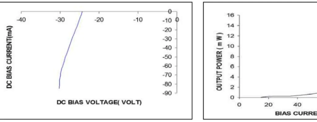
Fig.26 shows a block diagram of a Ka-band measurement test set up used for DC and RF characterization of IMPATT diode. Fig. 27 shows the DC V-I characteristic of the fabricated IMPATT diode. It is seen from the graph that the diode has a soft break down in the range of 25 -31 volt. A maximum current up to 85 mA is pushed through the device. Fig. 28 and Fig. 29 shows the plot of DC bias current vs output power and frequency
Fig.24. Schematic diagram of a Ka-band resonant cap waveguide cavity
Fig.25. Photograph of resonant cap oscillator
Spectrum Analyzer Frequency counter
10 dB 10 dB
DC Bias
Sliding short tuner
Voltmeter
Attenuator Isolator
IMPATT Oscillator Ampere meter
14. 65 mW has been achieved at a frequency of 35.70 GHz with a bias current of 85 mA and break down voltage of 31 volt.
6. Conclusion
In this paper the design of a SDR Ka-band IMPATT diode and then fabrication process steps following the diffusion technique are described in details followed by measurement of DC and RF characterization of developed IMPATT diode. A silicon (p+nn+) SDR IMPATT diode for Ka-band operation has been designed by using double iterative DC and Small signal simulation methods which involve simultaneous solution of Poisson’s equation and Carrier continuity equation under appropriate boundary conditions. The computation starts from the field maximum point in the depletion layers and proceeds towards the depletion layer edges. The current density and junction temperature have been taken to be 9×10⁷ A/m2 and 2250C respectively. The realistic field and temperature dependence of carrier ionization rates and the drift velocities at 2250 C and the effect of mobile space charge have been considered in the simulation. The design has been optimized to get the peak negative conductance at 36.5 GHz. Based on the DC and Small signal simulation, the authors have selected the thickness and resistivity of silicon epitaxial n/n+ wafers for fabrication of a (p+nn+)SDR Ka-band IMPATT Diode through diffusion route . The optimized process flow chart for realization of Ka-band SDR IMPATT is shown below.
A resonant cap cavity has been used for DC and RF characterization of the fabricated diode. A power output of 14. 65 mW at a frequency of 35.70 GHz has been achieved at a bias current of 85 mA with break down voltage of 31 volt. It is observed that the frequency of operation of the fabricated diode closely matches with the design frequency. The power and frequency can be optimized by thinning the substrate in the range of 5 -10 micron so as to minimize the effects of series resistance. To get the maximum output power at the desired frequency the operating dc bias current is in the range of 150 - 200 mA without the problem of thermal burnout of the device.
Fig. 27. V- I Characteristic of Ka-band IMPATT diode Fig. 28. Bias current Vs output power
IMPATT Diode Fabrication Process Flow
Acknowledgement
The first authoris thankful to Shri. S.K. Ray, DS & Director, Research Centre Imarat, Hyderabad, Shri. R. Das, Director, RF Systems, Dr. V.G. Borkar, Head, Antenna & Components Group and Shri. J.V. Prasad, Head, MMW Seekers & Sensors Division for their consistent support and encouragement for carrying out the research work.
References
[1] Roy, S.K., “Transit Time Device”, “Encyclopaedia of Electron Devices” vol. 24, Edited by John G. Webster, Wiley & Sons, New York 1999.
[2] Banerjee, J.P., Luy, J.F. and Schaffler, F., “Comparison of theoretical and experimental 60GHz silicon Impatt diode performance, Electronic Lett. (UK) vol 27, No.. 12, pp. 1049-1051 (1991).
[3] Russer, Peter., “Si and SiGe Millimeter-wave Integrated Circuits”, IEEE Trans. on MTT, Vol. 46, No. 5, pp. 590-603,1998.
[4] Sharfetter, D.L. and Gummel, H.K.,” Large signal analysis of a silicon Read diode oscillator”, IEEE Trans. Electron Devices, Vol ED- 16, No.1, pp.64-77, Jan.1969.
[5] Wolf, Helmut F., “Silicon Semiconductor Data”, Signetics Corporation, Pergamon Press, First Edition 1969.
[6] Howes, M. J. and Morgan, D.V., ‘Microwave Devices; Device Circuit Interactions’, A Wiley – Interscience Publication, Jhon Wiley & Sons, 1976.
[7] Gibbons, G., ‘Avalanche diode microwave oscillators’, Oxford University Press, Oxford 1973, Ch.4, pp. 45-65.
[8] Pal, Tapas Kumar., ‘A Tunable Millimeter wave (Ka-Band) IMPATT Source Using an Integrated Heat Sink cum Waveguide mount’, Patent no. 221758, INDIA, 15.02.2001.
[9] Roy, S.K., Banerjee, J.P. and Pati, S.P., “A computer analysis of the distribution of high frequency negative resistance in the depletion layer of IMPATT diodes”, Proceedings of the conference on Numerical Analysis of Semiconductor Devices (NASECODE IV) (Dublin, Republic of Ireland: Bolle Press), p. 494, 1985.
[10] Gummel, H. K. and Blue, J. L., “A small signal theory of avalanche noise in IMPATT diodes”, IEEE Trans. Electron Devices, vol. ED-14, pp.569-580.1967.
[11] Grant, W. N., “Electron and hole ionization rates in epitaxial silicon at high electric field”, Solid State Electron.,Vol. 16, p.1189,1973. [12] Canali, C., Ottaviani, G. and Quaranta, A.A., “Drift velocity of electron and holes and associated anisotropic effects in silicon”, J.
Phys. Chem. Solids, Vol. 32, p.1707. 1971.
[13] Kern, Werner., “The Evolution of Silicon Wafer Cleaning Technology” , J. Electrochem. Soc., vol.137, No. 6, June 1990, pp. 1887-1892.
[14] Nadtochiy, A., Podolian, A., Kuryluik,V. Kuryliuk, A., Korotchenkov,O., Schmid, Julian., and Schlosser , Viktor., ‘Electrical and Micromechanical Performance of Ultrasonically Cleaned Silicon Wafers’ Published, 27th
International Conference on Microelectronics (Miel 2010), NIS, Serbia, 16-19 May, 2010.pp. 261-264.
[15] Gale, G. W. and Busnaina, A. A., “Removal of particulate contaminants using ultrasonic and megasonics: A Review”, Particulate Sci. Technol., 1995, vol.13, pp.197 -211.
[16] Itano, Mitsushi., Kern, Frederick W., Mayashita, Jr. and Ohmi ,Tadahiro., “ Particle Removal from Silicon Wafer Surface in Wet Cleaning Process , IEEE Transactions on Semiconductor Manufacturing, Vol.6. No.3, Aug, 1993. Pp. 258 -269.
[17] William, Kirt R. and Muller Richard S., “Etch Rates for Micromachining Processing”, Journal of Microelectromechanical Systems, Vol.5. No.4, December 1996. pp. 256-269.
Low Temperature
Oxidation Drive in Diffusion
Pre-deposition of Boron
Mesa etching Photolithography Cr–Au Metallization of n+
side
Chip separation Die/wire Bonding
and packaging RF characterization Cr-Au Metallization
of p+
side
Electroplating of metalized p+
side Thinning of n
+
side Wafer cleaning Activation of Boron
Authors
Shri Tapas Kumar Pal, born in October, 1976 at Kolkata, obtained his M.Sc degree in Physics with
specialization in Microwaves from University of Calcutta in 1999. He has worked as a Senior Research Fellow and Senior Scientist at Centre of Advanced Study in Radiophysics & Electronics, University of Calcutta for a period of 2.5 years from Feb 2000 onwards. Later he worked as an Examiner of Patents & Designs at Patent Office, Kolkata till July 2005. Presently he is working as a Scientist ‘D’ at Research Centre Imarat, DRDO, Hyderabad. He is currently engaged in development of MMW Seekers and Sensors. His special interests are Design and Development of MMW IMPATT Diodes, Oscillators and Amplifiers and their computer simulations. He has also been pursuing Ph.D (Tech) Degree at Institute of Radiophysics & Electronics, University of Calcutta, on “Millimeter wave IMPATT Diodes and Oscillators”. He is a Life Member of IETE and Member of IEEE.
Dr J. P. Banerjee obtained B.Sc. (Hons.) and M.Sc. in Physics and Ph.D. in Radio Physics and