Broadband photocurrent enhancement in a-Si:H
solar cells with plasmonic back reflectors
Seweryn Morawiec,1,2,* Manuel J. Mendes,1 Sergej A. Filonovich,3 Tiago Mateus,3 Salvatore Mirabella,1 Hugo Águas,3 Isabel Ferreira,3 Francesca Simone,2 Elvira Fortunato,3 Rodrigo Martins,3 Francesco Priolo,1,2,4 and Isodiana Crupi1
1MATIS IMM-CNR, via S. Sofia 64, I-95123 Catania, Italy
2Dipartimento di Fisica e Astronomia, Università di Catania, via S. Sofia 64, I-95123 Catania, Italy 3CENIMAT/I3N, Departamento de Ciência dos Materiais, and CEMOP/UNINOVA, Faculdade de Ciências e
Tecnologia, Universidade Nova de Lisboa, 2829-516 Caparica, Portugal
4Scuola Superiore di Catania, Università di Catania, Via Valdisavoia 9, 95123 Catania, Italy *[email protected]
Abstract. Plasmonic light trapping in thin film silicon solar cells is a promising route to achieve high efficiency with reduced volumes of semiconductor material. In this paper, we study the enhancement in the opto-electronic performance of thin a-Si:H solar cells due to the light scattering effects of plasmonic back reflectors (PBRs), composed of self-assembled silver nanoparticles (NPs), incorporated on the cells’ rear contact. The optical properties of the PBRs are investigated according to the morphology of the NPs, which can be tuned by the fabrication parameters. By analyzing sets of solar cells built on distinct PBRs we show that the photocurrent enhancement achieved in the a-Si:H light trapping window (600 – 800 nm) stays in linear relation with the PBRs diffuse reflection. The best-performing PBRs allow a pronounced broadband photocurrent enhancement in the cells which is attributed not only to the plasmon-assisted light scattering from the NPs but also to the front surface texture originated from the conformal growth of the cell material over the particles.
As a result, remarkably high values of Jsc and Voc are achieved in
comparison to those previously reported in the literature for the same type of devices.
©2014 Optical Society of America
OCIS codes: (290.5850) Scattering, particles; (250.5403) Plasmonics; (350.6050) Solar energy.
References and links
1. H. A. Atwater and A. Polman, “Plasmonics for improved photovoltaic devices,” Nat. Mater. 9(3), 205–213 (2010).
2. F. Priolo, T. Gregorkiewicz, M. Galli, and T. F. Krauss, “Silicon nanostructures for photonics and photovoltaics,” Nat. Nanotechnol. 9(1), 19–32 (2014).
3. J. Müller, B. Rech, J. Springer, and M. Vanecek, “TCO and light trapping in silicon thin film solar cells,” Sol. Energy 77(6), 917–930 (2004).
4. K. Söderström, F. J. Haug, J. Escarré, C. Pahud, R. Biron, and C. Ballif, “Highly reflective nanotextured sputtered silver back reflector for flexible high-efficiency n–i–p thin-film silicon solar cells,” Sol. Energy Mater. Sol. Cells 95(12), 3585–3591 (2011).
5. M. J. Mendes, S. Morawiec, F. Simone, F. Priolo, and I. Crupi, “Colloidal plasmonic back reflectors for light trapping in solar cells,” Nanoscale (2014), doi: 10.1039/C3NR06768H
6. Z. Ouyang, X. Zhao, S. Varlamov, Y. Tao, J. Wong, and S. Pillai, “Nanoparticle-enhanced light trapping in thin-film silicon solar cells,” Prog. Photovolt. Res. Appl. 19(8), 917–926 (2011).
7. V. E. Ferry, M. A. Verschuuren, M. C. Lare, R. E. I. Schropp, H. A. Atwater, and A. Polman, “Optimized spatial correlations for broadband light trapping nanopatterns in high efficiency ultrathin film a-Si:H solar cells,” Nano Lett. 11(10), 4239–4245 (2011).
8. J. Park, J. Rao, T. Kim, and S. Varlamov, “Highest efficiency plasmonic polycrystalline silicon thin-film solar cells by optimization of plasmonic nanoparticle fabrication,” Plasmonics 8(2), 1209–1219 (2013).
10. C. V. Thompson, “Solid-state dewetting of thin films,” Annu. Rev. Mater. Res. 42(1), 399–434 (2012). 11. S. Morawiec, M. J. Mendes, S. Mirabella, F. Simone, F. Priolo, and I. Crupi, “Self-assembled silver
nanoparticles for plasmon-enhanced solar cell back reflectors: correlation between structural and optical properties,” Nanotechnology 24(26), 265601 (2013).
12. N. C. Lindquist, P. Nagpal, K. M. McPeak, D. J. Norris, and S.-H. Oh, “Engineering metallic nanostructures for plasmonics and nanophotonics,” Rep. Prog. Phys. 75(3), 036501 (2012).
13. K. R. Catchpole and A. Polman, “Design principles for particle plasmon enhanced solar cells,” Appl. Phys. Lett.
93(19), 191113 (2008).
14. F. J. Beck, S. Mokkapati, and K. R. Catchpole, “Light trapping with plasmonic particles: beyond the dipole model,” Opt. Express 19(25), 25230–25241 (2011).
15. S. Pillai, K. R. Catchpole, T. Trupke, and M. A. Green, “Surface plasmon enhanced silicon solar cells,” J. Appl. Phys. 101(9), 093105 (2007).
16. M. J. Mendes, A. Luque, I. Tobías, and A. Martí, “Plasmonic light enhancement in the near-field of metallic nanospheroids for application in intermediate band solar cells,” Appl. Phys. Lett. 95(7), 071105 (2009). 17. C. Eminian, F. J. Haug, O. Cubero, X. Niquille, and C. Ballif, “Photocurrent enhancement in thin film
amorphous silicon solar cells with silver nanoparticles,” Prog. Photovolt. Res. Appl. 19(3), 260–265 (2011). 18. H. Tan, R. Santbergen, A. H. M. Smets, and M. Zeman, “Plasmonic Light Trapping in Thin-film Silicon Solar
Cells with Improved Self-Assembled Silver Nanoparticles,” Nano Lett. 12(8), 4070–4076 (2012).
19. H. Tan, R. Santbergen, Y. Guangtao, A. H. M. Smets, and M. Zeman, “Combined optical and electrical design of plasmonic back reflector for high-efficiency thin-film silicon solar cells,” Phot. IEEE J. 3, 53–58 (2013). 20. A. Araújo, R. Barros, T. Mateus, D. Gaspar, N. Neves, A. Vicente, S. A. Filonovich, P. Barquinha, E. Fortunato,
A. M. Ferraria, A. M. B. Rego, A. Bicho, H. Águas, and R. Martins, “Role of a disperse carbon interlayer on the performances of tandem a-Si solar cells,” Sci. Technol. Adv. Mater. 14(4), 045009 (2013).
21. R. Martins, L. Raniero, L. Pereira, D. Costa†, H. Águas, S. Pereira, L. Silva, A. Gonçalves, I. Ferreira, and E. Fortunato, “Nanostructured silicon and its application to solar cells, position sensors and thin film transistors,” Philos. Mag. 89, 2699–2721 (2009).
22. R. Martins, P. Almeida, P. Barquinha, L. Pereira, A. Pimentel, I. Ferreira, and E. Fortunato, “Electron transport and optical characteristics in amorphous indium zinc oxide films,” J. Non-Cryst. Solids 352(9-20), 1471–1474 (2006).
23. P. Barquinha, G. Gonçalves, L. Pereira, R. Martins, and E. Fortunato, “Effect of annealing temperature on the properties of IZO films and IZO based transparent TFTs,” Thin Solid Films 515(24), 8450–8454 (2007). 24. R. S. A. Sesuraj, T. L. Temple, and D. M. Bagnall, “Optical characterisation of a spectrally tunable plasmonic
reflector for application in thin-film silicon solar cells,” Sol. Energy Mater. Sol. Cells 111, 23–30 (2013). 25. T. L. Temple and D. M. Bagnall, “Broadband scattering of the solar spectrum by spherical metal nanoparticles,”
Prog. Photovolt. Res. Appl. 21, 600–611 (2013).
26. M. J. Mendes, E. Hernández, E. López, P. García-Linares, I. Ramiro, I. Artacho, E. Antolín, I. Tobías, A. Martí, and A. Luque, “Self-organized colloidal quantum dots and metal nanoparticles for plasmon-enhanced intermediate-band solar cells,” Nanotechnology 24(34), 345402 (2013).
27. C. Pahud, O. Isabella, A. Naqavi, F.-J. Haug, M. Zeman, H. P. Herzig, and C. Ballif, “Plasmonic silicon solar cells: impact of material quality and geometry,” Opt. Express 21(S5), A786–A797 (2013).
28. H. Sai, K. Saito, and M. Kondo, “Enhanced photocurrent and conversion efficiency in thin-film microcrystalline silicon solar cells using periodically textured back reflectors with hexagonal dimple arrays,” Appl. Phys. Lett.
101(17), 173901 (2012).
29. J. Zhu, C.-M. Hsu, Z. Yu, S. Fan, and Y. Cui, “Nanodome solar cells with efficient light management and self-cleaning,” Nano Lett. 10(6), 1979–1984 (2010).
30. P. Kowalczewski, M. Liscidini, and L. C. Andreani, “Light trapping in thin-film solar cells with randomly rough and hybrid textures,” Opt. Express 21(S5), A808–A820 (2013).
31. S. Calnan and A. N. Tiwari, “High mobility transparent conducting oxides for thin film solar cells,” Thin Solid Films 518(7), 1839–1849 (2010).
32. J. A. Thornton, “High Rate Thick Film Growth,” Annu. Rev. Mater. Sci. 7(1), 239–260 (1977).
33. M. Adamov, B. Perović, and T. Nenadović, “Electrical and structural properties of thin gold films obtained by vacuum evaporation and sputtering,” Thin Solid Films 24(1), 89–100 (1974).
34. D. Depla, S. Mahieu, and J. E. Greene, “Chapter 5 - Sputter Deposition Processes,” in Handbook of Deposition Technologies for Films and Coatings (Third Edition), P. M. Martin, ed. (William Andrew Publishing, 2010), pp. 253–296.
1. Introduction
back reflector in substrate configurations [4]. The texturing approach is limited by the surface roughness that it introduces which contributes to the creation of defects and increased recombination in the bulk and surface of the silicon layers, thereby deteriorating the electrical performance of the cells. Therefore, recently there is a growing interest in the application of subwavelength metallic nanoparticles (NPs) for light trapping in TF solar cells [5–8] as they can scatter light efficiently over a broad wavelength range of the solar spectrum, due to the localized surface plasmon (LSP) resonances, with the theoretical possibility of exceeding the classical
4
n
2 limit of geometrical optics [5, 9].To be directly applicable in the photovoltaic industry, the NPs fabrication method needs to be reliable, low-cost and scalable up to square meter sizes. Therefore, self-assembly methods attract much attention, amongst which the most commonly used is the solid state dewetting (SSD) process [10, 11] (deposition of a precursor thin film followed by thermal treatment). Silver (Ag) is the metal of choice for the NPs as it enables high radiative efficiency and low imaginary permittivity in the visible and near-infrared (NIR) [12]. The scattering and absorption properties of the NPs are strongly dependent on their geometry (size and shape) and on the refractive index of the surrounding medium [13–16]. Thus, the proper design of the NPs and the device structure is essential to maximize the scattering and minimize absorption (termed parasitic absorption) over the wavelength range important for light trapping. The optical losses in the NPs at short wavelengths can be suppressed by placing them on the rear side of the solar cell, so that they interact only with the long-wavelength photons which are not absorbed during the first pass through the cell absorber material. Therefore, the NPs are preferentially located between the silicon and the back reflector (BR), forming a so-called plasmonic back reflector (PBR) [17].
Recently, Tan et. al. [18] have demonstrated that SSD self-assembled Ag NPs in a PBR configuration can provide light trapping performance comparable to state-of-the-art random texturing in single-junction TF hydrogenated amorphous silicon (a-Si:H) solar cells. Nonetheless, the morphology and optical properties of the self-assembled NPs are strongly sensitive to the fabrication conditions [11]. It is thus important to investigate the optical performance of the PBRs according to the range of parameters of the fabrication process, with the aim of optimizing their light trapping efficiency. In this paper, the optical properties of several PBRs formed with distinct fabrication parameters are analyzed and correlated to the photocurrent improvements that they produce in a-Si:H cells. The tuning of parameters allowed us to achieve a pronounced broadband photocurrent enhancement in the cells. In particular, the best-performing devices obtained in this work show high values of short circuit current density (Jsc = 15.75 mA/cm2) and open circuit voltage (Voc = 0.85 V) in comparison with those reported so far for plasmon-enhanced a-Si:H solar cells with self-assembled nanoparticles [17–19].
2. Experimental details
The thicknesses of the Ag and AZO layers are determined from Rutherford Backscattering
Spectrometry (RBS, 2.0 MeV He+ beam) in high resolution mode. The morphology of the
NPs is investigated by Field Emission Scanning Electron Microscopy (SEM – Zeiss Supra 25 microscope). The distributions of NPs were determined by digital analysis of SEM images conducted with the Gatan Digital Microscope software package. The surface morphology of a PBR with NPs formed from a 8 nm Ag precursor film is shown in the tilted SEM of Fig. 1(b). The optical properties of the PBRs, in terms of total and diffuse reflection (RTotal and RDiff, respectively), are measured using a Varian Cary 500 double-beam scanning UV-Vis-NIR spectrophotometer equipped with a 4-inch integrating sphere.
Fig. 1. (a) Schematic drawing of a plasmonic back reflector (PBR) with the structure: Glass substrate/100nm Ag mirror/40nm AZO spacer/Ag NPs/80nm AZO cover. (b) 70° tilted SEM image of the surface morphology of a PBR with NPs formed from a 8 nm thick Ag film annealed at 400 °C for 1 h, covered with a 80 nm AZO layer.
The n-i-p a-Si:H solar cells are deposited on the PBRs at a temperature of 170 °C using a multi-chamber plasma-enhanced chemical vapor deposition (PECVD) system [21], followed by the sputter deposition of the indium doped zinc oxide (IZO) front contact [22, 23]. Finally,
in order to improve the electrical performance, all the cells are annealed in low vacuum at 150 °C for 2 h. The devices are characterized by measuring the J–V curves, under AM1.5G
(100mW/cm2) illumination in a Spire Sun Simulator 240A, and external quantum efficiency (EQE) in short-circuit condition in the 350–800 nm wavelength range with a 10 nm wavelength interval between each measured data point. The open-circuit voltage (Voc) and fill factor (FF) of the cells are extracted from the J-V curves, and the short-circuit current density (Jsc) is determined from the integration of the EQE convoluted with the AM1.5G photon flux.
3. Results and discussion
3.1 Optical properties of plasmonic back reflectors
The morphology of the NPs has a strong impact on the optical properties of the PBRs and can be tuned by several parameters, such as the thickness of the precursor Ag film, annealing temperature and annealing time. It is generally desirable to prevent the formation of small (diameters < 60 nm) or irregularly-shaped NPs, as they are known to increase the parasitic absorption. At the same time, big NP sizes (heights > 200 nm) are not desirable as they can degrade the electrical properties of the cells due to the roughness induced in the Si layers [19]. The impact of the AZO spacer layer thickness on the scattering and parasitic absorption was
recently investigated by Sesuraj et. al. [24] who reported an optimum value in the range of 40 – 50 nm, depending on the size of the NPs. Tan et. al. [19] reported that a AZO cover layer
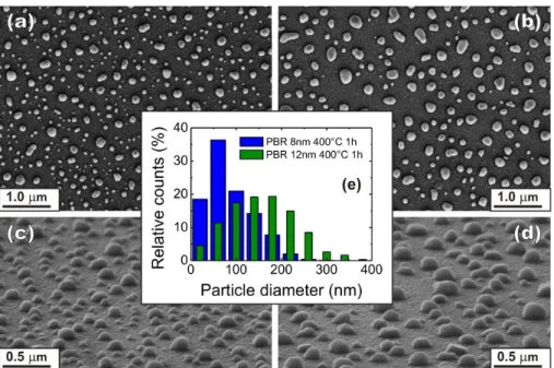
Fig. 2. (a-b) Planar and (c-d) 70° tilted SEM micrographs of uncovered NPs formed, respectively, from 8 and 12 nm thick Ag films annealed at 400 °C for 1 h. (e) Histogram of relative counts (counts normalized to the total number of NPs), as a function of the NPs’ in-plane diameter, for the NPs presented in the micrographs.
Figure 2 depicts the morphology of the NPs formed from 8 [Figs. 2(a) and 2(c)] and 12 nm [Figs. 2(b) and 2(d)] thick Ag films, in the same annealing process (400 °C for 1 h). From the analysis of the tilted SEM images [Figs. 2(c) and 2(d)], it was found that most NPs are roughly semi-spherical and tend to flatten out their shape with increasing size. The corresponding relative counts distribution of the NPs’ in-plane diameters is shown in Fig. 2(e). Comparing the two samples, the nanostructure formed from 8 nm of Ag contains a higher number of particles with diameter lower than 80 nm. The mean surface coverage [11], increases from 136 ± 4 to 206 ± 2 nm when the precursor film thickness is increased from 8 to 12 nm. Thicker precursor films could result in less uniform NP geometries with bigger NP sizes [11] which can be disadvantageous due to the increased roughness that they produce in the solar cell material.
Fig. 3. (a) Total and (b) diffuse reflection of the plasmonic back reflectors (PBRs) with NPs formed from 8 (circles) and 12 nm (triangles) thick Ag films annealed at 400 °C for 1 h, before (solid symbols) and after (open symbols) the deposition of the AZO cover layer. The RTotal and
RDiff of a flat BR reference (without NPs) are also shown (open diamonds) for comparison. The
wavelength range important for light trapping in a-Si:H (600 – 800 nm) solar cells is indicated by the vertical dashed lines.
Figure 3 depicts the spectral behavior of the total and diffuse reflection of a reference flat back reflector and two PBRs with NPs formed from 8 and 12 nm thick Ag films, annealed in the same conditions (400 °C for 1 h), before and after the final deposition of the AZO cover layer. As expected, the reference BR shows nearly 100% RTotal and almost negligible RDiff
over the a-Si:H light trapping spectral window. The PBR with uncovered NPs formed from 8 nm of Ag shows a broad single peak resonance with maximum at 800 nm, while the 12 nm
one shows a double-peak behavior with maxima at 500 and 1050 nm. The embedment of the NPs in AZO results in, first, the decrease of RTotal, second, the increase of RDiff, and third, the spectral broadening of RDiff. Unexpectedly, the RDiff and RTotal of both PBRs become similar in the light trapping window after covering with AZO. The differences are more evident in the
NIR region as the RDiff plateau of the 12 nm PBR extends 300 nm further to longer
wavelengths, from 800 to 1400 nm.
related to the embedment of the NPs in the AZO are chiefly attributed to the change in effective refractive index of the material surrounding the NPs, which redshifts and increases both the scattering (higher RDiff) and the absorption (lower RTotal) cross sections of the NPs [25, 26].
At the LSP resonance frequencies, practically all the incident photons interact with the NPs as almost all the light that is not absorbed is reflected diffusively from the PBRs. Therefore, the main factor limiting the performance of the PBRs is the parasitic absorption. In this respect, there is a significant discrepancy between theoretical calculations and experimental results since, according to single-particle electromagnetic modeling, Ag NPs with sizes above 100 nm should exhibit dominant scattering and negligible absorption cross section [5, 11, 13, 14, 25]. Though the origin of the unexpectedly high absorption remains unclear, it can be attributed to dissipative interactions between the NPs themselves and between the NPs and the mirror, the roughness and sharp features of the NPs, and the possible polycrystalline nature of the NPs material [27].
The suitability of a particular PBR for application in thin film a-Si:H solar cells depends on its optical properties which can be characterized by the average total reflection (<RTotal>)
and the average diffuse reflection (<RDiff >) in the light trapping wavelength range from λ1
toλ2:
2
1 2 1
2 1 X X
R d R
λ
λ
λ λ
λ
λ λ
− = −
(1)
where X corresponds to Total or Diff.
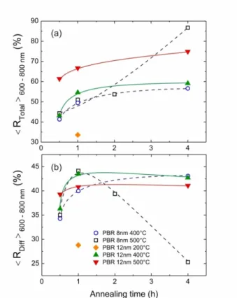
The dependence on annealing time of <RTotal>600 800nm− and <RDiff >600 800nm− is shown in
Fig. 4 for the PBRs with NPs formed from 8 and 12 nm thick Ag films annealed at 200, 400 and 500 °C. First of all, samples fabricated at 200 °C exhibit significantly worse performance, in both <RTotal>600 800nm− and <RDiff >600 800nm− , than those fabricated at 400 and 500 °C. Such
lower performance originates from the irregular nanostructures (irregular, island-like shaped NPs and high surface coverage – not shown here) which are obtained at low annealing temperatures [11]. This reveals the need to use a high temperature for NP formation, in accordance with Tan et al. [18].
The saturation behavior of <RTotal >600 800nm− and <RDiff >600 800nm− when the annealing
time exceeds 1 h is observed for all the samples, except that fabricated from a 8 nm thick Ag film annealed at 500 °C. Furthermore, the 12 nm samples show systematically higher values of total reflection than the 8 nm ones. The highest temperature of 500 °C used for NP formation was found to significantly increase the <RDiff >600 800nm− and decrease the
Total 600 800nm
R −
< > of the 12 nm samples, mostly due to the spectral shift of the plasmonic
Fig. 4. Annealing time dependence of the average (a) total and (b) diffuse reflection in the 600 – 800 nm wavelength range for the plasmonic back reflectors (PBRs) with NPs formed
from 8 (open symbols) and 12 nm (solid symbols) thick Ag films annealed at 200, 400 and 500 °C. The absolute differences in <RTotal>600-800nm and <RDiff>600-800nm observed between PBRs
fabricated in distinct batches, with the same fabrication parameters, were below 2.3%. That is the main error associated to the data points in the plots.
The optical performance of the PBRs analyzed in this section will be affected when they are implemented in solar cells, since the scattering properties of the NPs plus mirror system change when they are placed in the vicinity of a high refractive index material (silicon). The cell material generates additional back-reflected fields interacting with the NPs which can alter their polarizability and, consequently, the PBRs scattering spectra. Despite these effects, in previous studies of PBRs implemented in thin film Si cells [17–19] it has been observed that the reflection spectra of the PBR structures alone correlate with the light extinction and quantum efficiency enhancement spectra achieved when they are coupled to the cells. As such, the results presented in Fig. 4 constitute reasonable quantities for a preliminary evaluation of the PBRs, to determine the preferential fabrication parameters.
3.2 Plasmon-enhanced a-Si:H solar cells
To investigate the plasmonic light trapping in TF silicon solar cells, several PBRs with distinct optical performance were selected as substrates for the fabrication of n-i-p a-Si:H solar cells. Reference cells without NPs were fabricated in the same process on substrates containing only the flat Ag mirror and the AZO layers.
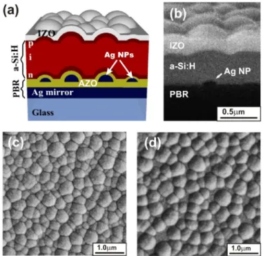
The structure of the a-Si:H n-i-p solar cells deposited on the PBRs is schematically shown
in Fig. 5(a) and in cross SEM (20° tilt angle) in Fig. 5(b). It consists of a stack of 33 nm n-type amorphous, 300 nm intrinsic amorphous, 13 nm type nanocrystalline and 7 nm
Fig. 5. Structure of a-Si:H n-i-p solar cell with plasmonic back reflector (PBR) shown (a) schematically and (b) in SEM cross section at a tilt angle of 20°. (c-d) SEM of the honeycomb-like surface texture of the top IZO layer of the devices fabricated with NPs formed from 8 and 12 nm thick Ag films annealed at 500 °C for 1 h and 400 °C for 4 h, respectively.
The conformal growth of silicon and IZO on top of the NPs resulted in the random honeycomb-like surface texture shown in Figs. 5(c)-5(d) for two of the best-performing PBRs, 8 nm 500 °C 1 h (c) and 12 nm 400 °C 4 h (d), respectively. The surface of the cell with NPs formed from 8 nm of Ag is denser and exhibits smaller features, in agreement with the NPs morphology observed by SEM. The rms roughness determined by atomic force microscopy (AFM) was of 25 and 28 nm for the top surface of, respectively, the 8 and 12 nm cells of Figs. 5(c) and 5(d).
The EQE curves of the cells fabricated on these two PBRs and on a flat BR reference are shown in Fig. 6. Both PBRs provide a broadband EQE enhancement relative to the reference cell, not only in the red-NIR light trapping window (600-800 nm) but also in the blue-green spectral range (430 – 570 nm). The improvement in the short wavelength range originates from the texture of the solar cells front surface, as in this spectral region all the incident light is absorbed in the Si layers during the first pass without interacting with the NPs. The light coupling provided by the honeycomb-like texture is more efficient than the reference flat IZO layer acting as a simple antireflection coating [28, 29]. For wavelengths longer than 600 nm, the EQE enhancement can have contributions from both the surface texture and the plasmon-assisted scattering from the Ag NPs; and the impact of the two mechanisms cannot be measured separately. However, previous computational studies indicate that moderate surface roughness should only significantly increase absorption in Si thin films for wavelengths roughly below 500 nm [30], whereas Ag NP structures can provide pronounced absorption enhancement only at longer wavelengths [13, 14]. Therefore, and considering the diffusion properties of the PBRs analyzed in section 3.1, the main light trapping effect leading to the observed photocurrent gains in the red-NIR range (600 - 800 nm) is attributed to LSP-assisted scattering.
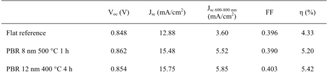
Table 1. Electrical parameters of the solar cells fabricated on two PBRs with NPs formed from 8 and 12 nm thick Ag films, in comparison with the reference cell deposited on a flat
back reflector (EQE curves shown in Fig. 6)*
Voc (V) Jsc (mA/cm2)
Jsc 600-800 nm
(mA/cm2) FF η (%)
Flat reference 0.848 12.88 3.60 0.396 4.33 PBR 8 nm 500 °C 1 h 0.862 15.48 5.52 0.390 5.20 PBR 12 nm 400 °C 4 h 0.854 15.75 5.85 0.403 5.42 *The Jsc 600-800 nm is the current density obtained from integrating the EQE curve, convoluted with the AM1.5G photon
flux, only in the 600-800 nm wavelength range.
The electrical parameters of the cells are listed in Table 1. The JSC value of 15.75 mA/cm2 and VOC of 0.85 V measured for the devices fabricated on the PBR with 12 nm Ag, annealed at 400 °C for 4 h, are among the highest values reported for plasmonic light trapping in a-Si:H solar cells with self-assembled NPs [17–19] due to the high photocurrent enhancement (22.3% for the total Jsc and 62.5% for the Jsc over the 600-800 nm range) provided by such PBR, without degrading the Voc of the cells.
The devices, however, suffer from low values of fill factor (FF), caused by both high series resistance (RS) and low shunt resistance (RP). The high RS should be mainly caused by
the relatively high resistivity (7.2x10⁻⁴ Ωcm) of the IZO top contact, compared to that (~10−4Ωcm) of state-of-art TCOs [31], and possible defects in the TCOs and doped Si layers.
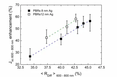
Fig. 7. Plot of short circuit current density enhancement as a function of the average diffused reflection (<RDiff >600 800nm− ) of the PBRs in the 600 – 800 nm wavelength range,
corresponding to the light trapping window of a-Si:H solar cells.
Figure 7 depicts the relation between the optical performance of PBRs, in terms of
Diff 600 800nm
R −
< > , and the Jsc enhancement in the corresponding wavelength range, based on
more than 40 solar cells. Each symbol corresponds to the average value of a set of 4 to 6 cells, while the error bars indicate the maximum and the minimum enhancement of the set. A linear relation between the Jsc 600-800 nm enhancement and <RDiff >600 800nm− was found for both 8 and
12 nm PBRs with approximately the same slope (2.75 ± 0.09 and 2.8 ± 0.4, respectively). The 8 nm PBRs, however, show systematically lower enhancement than the 12 nm ones mainly due to the lower total reflection, and hence higher parasitic absorption, in the 8 nm structures.
Furthermore, the 8 nm samples exhibit lower values of RDiff over the 600 – 700 nm
wavelength range, where light trapping effects contribute more pronouncedly to the generated photocurrent.
The clear linear relations shown in Fig. 7 prove that the EQE enhancement observed in the 600 – 800 nm region originates mainly from the scattering of light by the NPs sustaining plasmonic resonances. In addition, the extrapolation of the linear fits indicates that values of
Diff 600 800nm
R −
< > higher than 24.5% and 22.5%, respectively for 8 and 12 nm PBRs, are
required to compensate the intrinsic loses of light in the NPs and produce a positive Jsc 600-800 nm enhancement. This reveals the importance of the trade-off between beneficial
effects of scattering and negative effects of parasitic absorption on the solar cells’ photocurrent.
4. Conclusions
In conclusion, we investigate the optical properties of plasmonic back reflectors with self-assembled silver nanoparticles, formed by solid-state dewetting with distinct fabrication conditions, and their impact on the performance of n-i-p a-Si:H solar cells. The method used in this work to deposit the precursor Ag films by sputtering is distinct to the conventionally-used thermal evaporation process. This should allow a better crystalline quality of the NPs’ material and thus less energy dissipation at the LSP resonances. The PBRs produced in this way provide broadband quantum efficiency enhancement in the visible and NIR range which is attributed to both the cells front surface texture induced by the NPs shape and to plasmon-assisted scattering.
The best-performing solar cells were obtained with a PBR containing NPs formed from a 12 nm thick Ag film annealed at 400 °C for 4 h. Such PBR provided a pronounced 22.3% enhancement of Jsc (and 62.5% for the photocurrent in the 600-800 nm range), which allowed the achievement of high absolute values of Jsc = 15.75 mA/cm2 and Voc = 0.854 V relative to those reported so far for plasmon-enhanced a-Si:H solar cells. Although the devices suffer from low values of fill factor, no deterioration occurs due to the presence of the NPs since the PBR-enhanced cells have similar FF as the reference cells without particles.
The EQE response of more than 40 solar cells, deposited on distinct types of PBRs, was analyzed and correlated to the previously-measured light scattering properties of the PBRs. This allowed the determination of a linear relation between the average diffuse reflection of the PBRs, in the 600 – 800 nm wavelength range, and the corresponding Jsc enhancement. This reveals that the identification and the minimization of the parasitic absorption in the NPs is a crucial point for further improvement of plasmonic light trapping.
Acknowledgments