Photonic-structured TCO front contacts yielding optical
and electrically enhanced thin-film solar cells
Olalla Sanchez-Sobrado,* Manuel J. Mendes,* Tiago Mateus, João Costa, Daniela Gomes, Hugo Aguas, Elvira Fortunato, Rodrigo Martins
i3N/CENIMAT, Department of Materials Science, Faculty of Science and Technology, Universidade NOVA de Lisboa and CEMOP/UNINOVA, Campus de Caparica, 2829-516
Caparica, Portugal
*[email protected]; *[email protected]
Abstract
Wavelength-structured transparent conductive oxide (TCO) electrodes are highly promising to improve both the optical and electrical performance of photovoltaic (PV) devices, due to wave-optical light-trapping (LT) effects and higher TCO volume without increasing optical losses.
Herein we present a complete study of the benefits of microstructured IZO contacts applied on amorphous-silicon (a-Si) thin film solar cells. The IZO LT structures were integrated by an innovative colloidal lithography process on the front contact of the cells, resulting in enhancements of 26.7% in photocurrent, with respect to planar reference cells, when using an ultra-thin (30 nm) flat IZO layer between the LT structures and the a-Si absorber. However, the best efficiency enhancement (23.1%) was attained with an optimized thickness of 190 nm for this layer, due to a more favorable combination of optical and electrical gains.
In view of the application of this LT strategy in flexible PV devices operating under bending, the angular response of the cells was studied for 0-90º incidence angles. This showed that the LT enhancements are generally higher at oblique incidence, reaching 53.2% and 52%, respectively in photocurrent and efficiency, at ±70º angles with the
optimized flat IZO thickness of 190 nm; and 52.2% in efficiency at ±40º with the ultra-thin thickness of 30 nm. These results are among the highest gains reported thus far for LT-enhanced thin film solar cells.
Keywords: thin film photovoltaics, wave-optical light management, photonic-structured transparent electrodes, amorphous silicon solar cells, angular response of light trapping.
1 Introduction
Thin film solar cells (TFSC) have acquired notorious attention from the energy industry due to their thin absorber dimension, e.g. hundreds of nanometers thick in the case of hydrogenated amorphous silicon (a-Si:H), which favors their exploitation as photovoltaic (PV) devices for consumer-oriented portable and potentially-flexible power sources1,2.
Nevertheless, mainly due to the low thickness of their absorber layer, the photocurrent (and, thus, efficiency) of such devices is severely limited by insufficient sunlight absorption. To address this issue, different optical solutions have been proposed for light absorption enhancement in TFSCs3–8. High refractive index (n) particles and structures
with wavelength-scale dimensions have been considered the preferable light trapping (LT) solutions for integration in the illuminated face of the PV devices,3,9,10,4 due to their
remarkable ability for light in-coupling (anti-reflection) plus scattering towards the absorber medium. Recent theoretical works11,12 have demonstrated that up to ~50%
current enhancement is possible in TF Si cells using arrays of TiO2 (n=2.5-2.7)
pyramidal-like microstructured features patterned on the cells’ front. This optimized TiO2
-based LT geometry has been engineered by the authors, via a low-cost colloidal lithography (CL) procedure, and optically-tested on a-Si:H thin film absorbers which allowed the demonstration of pronounced broadband absorption enhancement (27.3% on spectral average) in the Si medium.9 CL is a particularly advantageous
nano/micro-pattern any material with the dimensions appropriate for efficient light trapping, and implemented in any type of solar cell with different absorbers (e.g. based in perovskites13,14, CIGS15, etc). In a subsequent work the authors have shown that, when
integrated on a-Si TFSCs, such TiO2-based LT structures fabricated by CL can lead to
notorious increments (up to 21.5%) in the short-circuit current density (JSC) but to less
pronounced enhancements (up to 13%) in the efficiencies, with respect to flat reference cells16. Although TiO
2 is an optically-favorable LT material for application in the cells’
front, due to its high real part of the refractive index and low imaginary part (little parasitic absorption), it is a dielectric with very low conductivity and, therefore, it is difficult to integrate with the front transparent conductive oxide (TCO) contact layer of the devices. When the microstructured TiO2 is applied over the cells’ front TCO, a refractive-index
mismatch is created which reduces the light in-coupling towards the absorber and increases reflection losses.
Therefore, a promising solution to circumvent this issue is to develop optically-enhanced TCO materials that can perform the double role of front electrode and LT medium17,
which can bring several advantages: 1) optically, this avoids refractive index mismatches when the light enters the cell, thus eliminating the aforementioned reflection losses; 2) electrically, the use of a microstructured TCO allows higher volume of electrode material without optical losses, thus enabling lower sheet resistance of the front contact; 3) industrially, it avoids the use of another distinct material for the LT medium, since the front TCO can assume such role, thus reducing the process complexity and costs. The work presented here studies this solution, focusing on microstructured IZO top contacts applied on a-Si TFSCs, and evaluating the impact on the photovoltaic performance of the devices. Given the important potential of this technology in the field of portable/flexible electronics, in which the cells are mainly illuminated at oblique incidence during operation, a complete analysis of the angular response of the devices
has also been performed, comparing the response of LT-enhanced cells with that of flat (unpatterned) references.
2 Experimental methods
2.1 Solar cell fabricationSubstrates preparation
Glass slides were cut with 2.5 x 2.5 cm, followed by washing with a MICRO-90 concentrated cleaning solution and rinsed with distilled water. After sonication in distilled water for 15 minutes, the substrates were rinsed in acetone and ethanol. Finally, they were dried under a nitrogen flow.
Deposition of rear contact
The aluminum (Al) rear electrode of the SCs, with a thickness of 120 nm was deposited on glass substrates using resistive thermal evaporation, applying a current of 160 A under 10−6 mbar vacuum. The deposition rate was 0.3 nm/s.
The Al film was coated with an aluminum zinc oxide (AZO) layer of 60 nm, deposited by radio frequency (RF) magnetron sputtering for 18 min using the conditions listed in Table 1. TCO Material O2 Gas Pressure (mbar) Ar Gas Pressure (mbar) Power (W) Deposition rate (nm/min) Distance to the sample (cm) Target AZO 1x10⁻⁶ 1.8x10⁻³ 75 3.3 15 Al2O3/ZnO 99.99% purity, 2.8” diameter IZO 1x10⁻⁵ 1.5x10⁻³ 50 2.9 15 In2O3/ZnO 99.99% purity, 3” diameter
Table 1. Experimental conditions used during the different RF sputtering deposition processes of
the TCO materials composing the devices. A 20 min pre-sputtering was performed before each deposition.
Deposition of a-Si:H layers
The samples were then transferred to an Electtrorava plasma-enhanced chemical vapor deposition (PECVD) system where the silicon layers were deposited according to the n-i-p structure to form the cell junction. A mixture of SiH4 and H2 defines the hydrogen
dilution parameter (DH (%) = [H2/(H2+SiH4 )] ×100). In the case of the intrinsic silicon thin
film a DH = 95% was used with a deposition pressure (Pgas) of 1 Torr and a power density (PW) equal to 69.4 mW/cm2 to obtain a thickness of ~230 nm. Adding
trimethylboron (TMB,B(CH3)3) or PH3to the mixture of SiH4 and H2 produced p- or
n-layers, respectively. A p-a-Si:H layer of 12 nm was deposited with a DH = 74.9%, RTMB = TMB/(TMB+SiH4) = 1.3%, a Pgas = 1.05 Torr and a PW = 48.6 mW/cm2. As for the
n-a-Si:H layer, the parameters were: DH = 95.0%, RPH3 = PH3 /(PH3+SiH4) = 1.3%, Pgas
= 1 Torr, PW = 55.5 mW/cm2 and the corresponding thickness was 30nm.
Deposition of front contact and SC area delimitation
Transparent conductive oxide layers made of IZO with different thicknesses (see Table 3) were deposited by RF magnetron sputtering over the a-Si layers, for time periods comprised between 4 and 80 min employing the conditions listed in Table 1.
To delimit SCs of 3 mm of diameter, the deposition of the IZO front electrodes was carried out using a metallic mask with circular holes of that diameter. Afterwards, SF6 plasma
etching treatment was conducted to remove the a-Si material all over the substrate except in the SCs areas, defined by the IZO contact, which allow access to the AZO-Al back contact.18 This plasma etching process is performed to finalise the devices, namely
to remove the a-Si material in the regions of the sample between the solar cells, i.e. between the areas where the top IZO layer (acting as an etch-stopper) was deposited
via the predefined mask. In this way, this step delimits the areas of the solar cells to 3 mm circles on the sample and reveals the AZO-Al rear contact in the inter-cells regions. SF6 was chosen because it does not affect the IZO in the dry etching process. Finally, to
assist in the external connection to the front TCO contact, two Al pads were deposited at both sides of each SC using another mask.
2.2 Colloidal lithography patterning of photonic coatings
The soft-lithography method used in this work to fabricate the microstructured TCO contacts is briefly explained below, but more detailed descriptions can be found in previous works by the authors9,16.
Assembly of the colloidal monolayer
Colloidal suspensions of polystyrene (PS) spheres were used, purchased from Microparticles GmbH, with a diameter of 1.6 µm dispersed in a mixture of water and ethanol (1:3) at a solution concentration of 2.5% wt. A monolayer of such microspheres was directly deposited on the top flat IZO-coated surface of the SCs following a Langmuir-Blodgett (LB)19 wet-coating methodology. This process started by depositing
400 µl of the colloidal suspension in the interface between water and air, using a syringe. The barriers of the LB system were then closed at a controlled speed of 10 mm/min, driving the floating spheres to self-assemble at such interface in an ordered close-packed hexagonal array. Afterwards, the obtained monolayer was transferred to the surface of the prepared samples by dip coating, with a withdrawal speed of 2 mm/min.
Shaping of colloidal array
The geometry of the colloids, 1.6 µm initial diameter, was tuned by exposing the deposited monolayer to O2 reactive ion etching (RIE) for 150 seconds employing the
conditions in Table 2. The monolayer array of etched colloids acts as the mask to shape the material deposited in the subsequent step.
RIE gas Etched Material Time (s) RIE Power (W) GasPressure (mTorr) Plasma Flow (sccm) O2 Polystyrene 150 90 250 20 Ar/CF4 IZO 90 100 15 4/16 SF6 a-Si:H 240 30 30 10
Table 2. Conditions used during the different reactive ion etching (RIE) processes.
IZO infiltration
The IZO material of the photonic front structures was then deposited by RF sputtering for 4.5 hours, employing the conditions given in Table 1, infiltrating in the inter-spaces between the etched PS colloids.
Lift-off of colloids
The last step of the microstructure fabrication procedure consisted in removing the etched PS particles by sonicating the samples in a toluene bath for 1 minute. Previously, an Ar/CF4 RIE process (see Table 2, row 2) was applied to remove the top capping layer
of IZO over the colloids and facilitate the subsequent dissolution of their PS material in the toluene bath.
2.3 Characterization
Scanning Electron Microscopy
The morphological characterization of the geometrical dimensions of the different components of all fabricated samples was performed by Scanning Electron Microscopy (SEM) measurements using a CARL ZEISS AURIGA Cross Beam workstation.
The optical measurements were performed with a UV-VIS-NIR scanning spectrophotometer (PERKIN ELMER lambda 950), using a 15 cm diameter integrating sphere to obtain the total reflectance (RT) spectra of the solar cells. Total absorptance
spectra were estimated by using the general formula: AT (%) = 100 - RT (%). The optical
angular measurements were taken by adapting a sample holder with a goniometer inside the integrating sphere.
Photovoltaic response
The measurements of the I-V curves of the fabricated solar cells were performed with a LED Sun Simulator (Oriel VeraSol LSH-7520) composed of multiple LEDs at 19 individual wavelength intervals spaced over the spectrum from 400 to 1100 nm, supplying a 1-Sun illumination certified AAA in a 51 x 51 mm area. The external quantum efficiency (EQE) measurements were performed using a Newport QuantX-300 system, equipped with a Xenon lamp of 100 W, at wavelength intervals of 10 nm with a nominal illumination spot size of 0.8 x 1.1 mm. In both cases, angular measurements were taken by adapting the sample holder with a goniometer.
3 Results and discussion
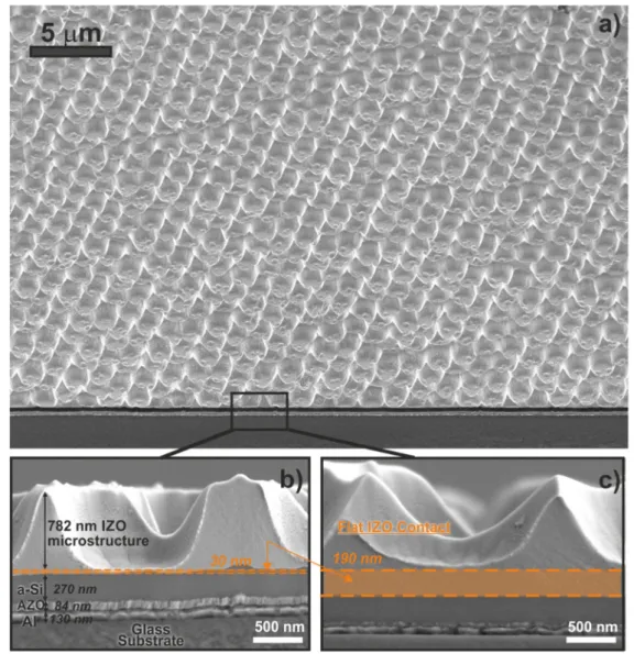
Figure 1 depicts the microstructured IZO top contact layer patterned on the a-Si TFSCs, following the colloidal lithography (CL) process described in the experimental section and in previous contributions9. Briefly, it consists in depositing a monolayer of
close-packed colloidal polystyrene (PS) microspheres by Langmuir Blodgett19. Then, the
microspheres are reduced and shaped by applying an O2 reactive ion etching (RIE)
process, thus resulting in a non-closed-packed hexagonal array of spheroids that acts as mask. The voids between spheroids were infiltrated with IZO deposited by sputtering. The last step consists in lifting off the PS microspheres by combining a CF4 RIE with a
cells’ top surface. The resulting hexagonal arrays of ~850 nm tall pyramidal-shaped features uniformly cover the full active area of the solar cells, with a pitch defined by the 1.6 µm initial diameter of the PS microspheres, as seen in Fig. 1.
Figure 1.(a) Tilted SEM image of a solar cell, composed of the layer structure: glass
(substrate)/Al+AZO (rear contact)/a-Si:H (n-i-p absorber)/IZO (front contact), coated with the top LT structure (made of IZO) that uniformly covers the entire illuminated area of the solar cell. The pyramidal-like features of the LT structure have an average height of 850 nm, and they were fabricated using a mask of PS spheres with 1.6 µm diameter.(b-c) SEM cross sections of devices with two different thicknesses of the flat IZO layer (30 and 190 nm, respectively) between the a-Si:H absorber and the front LT structures.
These wavelength-sized pyramidal microstructures can exhibit strong anti-reflection and light scattering effects at the cells’ front, as described in previous theoretical studies11,12,
such optical effects are maximized when the base of the pyramidal features is directly attached to the high-index Si absorber medium. Nevertheless, as observed in previous experimental tests16, such optically-optimum case does not allow an electrically-effective
front contact, which can only be realized with an additional flat IZO layer deposited prior to the patterning of the microstructured IZO. Therefore, a planar IZO thin film is required between the base of the pyramidal LT structures and the a-Si layer (see Fig. 1b, c), which reduces the LT effects but is necessary to allow a sufficiently low sheet resistance at the front contact. As such, a crucial compromise must be found in the present LT design, since the thicker is this flat IZO layer the higher will be the conductance of the top electrode but the lower will be the optical gains provided by the LT structure.
To evaluate the role played by the flat IZO layer, and to find the optimum electrical vs. optical compromise, a set of seven TFSCs were fabricated with different thicknesses of this layer separating the a-Si absorber from the LT features, which are indicated in Table 3. The performance of these devices is compared further below with that of seven reference cells produced in the same batches, having the same thicknesses of the flat IZO layer but with no LT microstructure patterned on top. The minimum thickness tested was 30 nm since it is necessary to have a conductive flat layer, covering the entire surface beneath the LT structures, to realize reasonably transparent electrodes at the cell front. It was observed that lower thicknesses would hardly allow measurable I-V characteristics of the cells.
Solar cell label: S30 S60 S95 S130 S190 S220 S250
IZO deposition time
(min) 4 14.5 25 47 58 70 80
Table 3. Sputtering deposition time and resulting thickness of the different flat IZO layers,
composing the top contact of the solar cells, located between the a-Si:H absorber and the IZO LT structures.
Figure 2 presents an analysis of the variation of the short-circuit current density (JSC) and
power-conversion efficiency (PCE) of these test cells, extracted from their JV characteristic curves measured under 1-Sun illumination (see section 2.3). The SCs integrating the LT structures produce currents and efficiencies consistently higher than the non-structured reference SCs, as expected, with only one exception for the case of the 250 nm thickness of the flat IZO in which there is still a JSC gain but an overall
efficiency loss. Nonetheless, there is in general a considerable gain in PCE due to LT, which is higher in some cases than the JSC gain. This contrasts with most LT applications
so far, in which the enhancements have been chiefly attained in the photocurrent (due to increased light absorption), while the electrical parameters (open-circuit voltage, VOC,
and fill-factor, FF) are usually reduced4,10,16. However, here the fact that the PCE is even
more enhanced than the JSC shows that our innovative strategy, based on a
wavelength-structured TCO, produces both optical and electrical benefits. This is because it enables the application of a higher volume of TCO material at the front transparent contact (thus decreasing its sheet resistance) while also creating LT effects (anti-reflection plus light scattering) that boost the broadband absorption in the a-Si layer. This is most notorious in the case of the 95 nm flat IZO, where the PCE enhancement is superior to the JSC
enhancement due to the fact that the improvement attained with the inclusion of the LT structure is mainly of electrical (rather than optical) nature. Here the efficiency gain is chiefly a consequence of the reduction of the sheet resistance of the front IZO contact due to the presence of additional IZO material composing the LT structure; while the photonic effects caused by such structure have relatively less expression in the light absorption occurring in the a-Si layer. Also, in the case of the thinner flat IZO thickness
(S30), the LT structure is implemented quite close to the a-Si absorber and highly reinforces the conductance of the ultra-thin (30 nm) TCO top contact.
Looking at the trends of the gains attained in JSC and PCE, shown in Fig. 2b as a function
of the thickness of the flat IZO layer beneath the LT structures, it is notorious that the enhancements are not monotonous with increasing thickness. The JSC and PCE
enhancement curves first decrease up to an IZO thickness of 95 and 60 nm, respectively, and then increase up to 190 nm where there is a local maximum in the curves. Such variation is a consequence of two optical effects:
1) The flat IZO layer acts as an anti-reflection coating (ARC) mainly in the planar regions between the pyramidal features of the LT structures. As is known for planar single-layer ARCs applied on a-Si TFSCs11,20, they lead to a first minimum in reflection for a layer
thickness around 70 nm (corresponding to λ/4nARC) and to a second minimum around
200 nm thickness. Therefore, the JSC of the reference cells is highest at the 60 nm and
190 nm IZO cases, since these are the deposited thicknesses closer to the aforementioned values;
2) The thicker the flat IZO layer the higher is the separation between the LT structures and the Si absorber, so the lower are the LT gains. This second effect is most prominent for the thinner IZO layers, establishing a small separation, so the highest enhancement in JSC (26.7%) is attained for the minimum 30 nm thickness. Here the gain in broadband
light absorption in a-Si is highest, leading to a quite remarkable photocurrent enhancement value in comparison with the current state-of-art of photonic-enhanced a-Si SCs.12,21
For the thicker IZO layers, effect 2) is less dominant, so the enhancement curves present a local peak at 190 nm thickness due to the second maximum of the ARC effect 1).
Figure 2. a) Measured values of photocurrent (JSC) and efficiency (PCE) for the test solar cells of Table 3 with distinct thickness of the flat IZO top layer separating the a-Si absorber from the front LT structures (see Fig. 1). The dashed bars correspond to the respective planar references without the photonic structures. b) Evolution of the enhancement of the JSC and PCE with the flat IZO layer thickness. The value below the horizontal dotted line corresponds to negative enhancement.
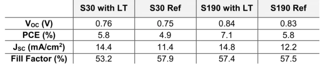
Considering now the absolute values of JSC and PCE in Fig. 2a, there are two prominent
cases highlighted in color, corresponding to the 30 nm (S30) and 190 nm (S190) flat IZO thicknesses. Table 4 summarizes the parameters of the I-V curves of these cases. In S30, the LT features are placed quite close to the a-Si layer, so the attained JSC is high,
IZO layer connecting the front contact. The application of the IZO-based LT structures reinforces the conductance of such contact due to the incorporation of additional IZO material, so the PCE of this cell is highly enhanced due to both optical and electrical improvement. In the case of S190, the larger separation between the LT features and the a-Si is compensated by both the electrical reinforcement of the IZO top contact and the optimized ARC action of the flat IZO layer, thereby enabling the highest PCE gain (23.1%) and highest absolute values in JSC (14.8 mA/cm2) and PCE (7.2%) attained in
this study.
S30 with LT S30 Ref S190 with LT S190 Ref VOC (V) 0.76 0.75 0.84 0.83
PCE (%) 5.8 4.9 7.1 5.8
JSC (mA/cm2) 14.4 11.4 14.8 12.2
Fill Factor (%) 53.2 57.9 57.4 57.5
Table 4. Main parameters of the I-V characteristics of the most relevant LT-enhanced TFSCs
analyzed in this work, and of their respective reference SCs (Ref) without LT.
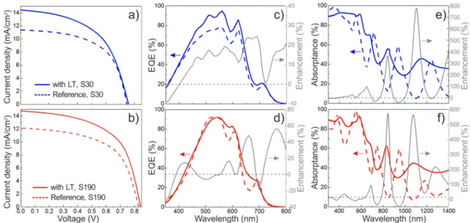
For a more in-depth analysis, Fig. 3 shows the J-V characteristic curves as well as the total absorption and quantum efficiency (QE) spectra of the reference and LT-enhanced cells of samples S30 and S190. Figs. 3c, d reveal that the LT structures lead to a remarkable broadband enhancement of the total light absorbed by the devices, along most of the wavelength range of study (350-1400nm). Nevertheless, the “useful” absorption occurring in the a-Si layer can only be ascribed to the lower (<800 nm) portion of the spectrum, corresponding to the photocurrent-generation wavelength range indicated by the QE spectra of Fig. 3c, d. The total absorption at larger NIR wavelengths is mostly parasitic, occurring chiefly at the front and rear contacts. The gains in useful absorption due to the LT structures translate into a general increment of the QE spectra and of the JSC value.
Figure 3. J-V curves, in a,b), external quantum efficiency, in c,d), and optical absorptance, in e,f),
obtained for samples S30 (blue lines) and S190 (red lines). In all plots the solid lines correspond to the photonic-structured solar cells and the dashed ones to their respective planar references, being the enhancements represented by the grey lines in c-f). Horizontal dashed lines in c, d, e and f) indicates 0% of enhancement.
Angular response
The previously analyzed opto-electronic response of the solar cells was measured under illumination incident normal to the cells. Nevertheless, for practical PV applications it is important to analyze the cells’ response for oblique incidence, particularly with thin film devices that are usually not mounted on sun-tracking platforms. In addition, if the cells are integrated on flexible substrates, they can operate in a bent state having a range of incidence angles shining throughout their active area. Therefore, if their response is not omnidirectional, a JSC reduction in one portion of the active area can cause an overall
drop in the total current supplied by the cells. In view of this, it is advantageous to implement LT structures able to provide JSC values as high and independent as possible
TFSCs, as they can be much more flexible than those with thicker absorbers such as c-Si wafer-based cells.
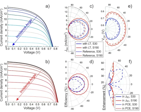
The results of the angle-resolved opto-electronic response are summarized in Fig. 4 for the samples S30 (blue lines) and S190 (red lines) analyzed in Fig. 3. Figs. 4a, b presents the evolution of the J-V curves with the incidence angle, showing that the generated current and voltage are maximum for 0º (light impinging normally to the cells’ surface) and minimum for 90º (light impinging parallel to the surface). As expected, when the incidence angle increases there are increased loses by reflection which reduce the power output. The dependence of the JSC, PCE and VOC with the incidence angle are
shown by the polar plots of Figs. 4c, d, e respectively, while the enhancements in JSC
and PCE are depicted in Fig. 4f. When looking at Figs. 4c-e, it may appear that the presence of the LT structures has little influence on the angular response of the devices, as the angular trends of the JSC, PCE and VOC appear similar when comparing the
LT-enhanced (solid lobes) and reference (dashed lobes) devices. However, when observing the angular response of the enhancement values in Fig. 4f, it is clear that the LT structures are even more beneficial for oblique illumination. For S190, the gains in PCE and JSC are quite similar and increase for angles away from the normal incidence (0º),
reaching respectively 52% and 53.2% at ±70º angle. For S30 the gain in JSC follows a
similar trend, but the PCE enhancement becomes even higher with increasing angle, peaking in 52.2% at ±40º angle, which is mainly due to the fact that the efficiency of the planar reference cell decreases more with increasing angle than that of the LT-enhanced cell. In this case it is particularly evident the superior PCE gains relative to the JSC ones,
which is not common when implementing LT schemes, as previously commented, since they are mainly targeted for absorption (hence photocurrent) enhancement. Nevertheless, here the high PCE gains result from the pronounced improvement produced in the conductance of the front transparent contact while also boosting absorption in the underneath Si material.
Figure 4. (a,b) Evolution with the incidence angle (from 0º to 90º relative to the cells’ surface
normal incidence with a step of 10º) of the J-V curves corresponding to samples S30 (a) and S190 (b). (c-e) Polar plots representing the angular response of the solar cells S30 (blue lines) and S190 (red lines) in terms of JSC (c), PCE (d) and VOC (e). The solid lines correspond to the
photonic-structured solar cells and the dashed ones to their respective planar references. f) Polar plot of the enhancements of JSC (solid lines) and PCE (dashed lines) for solar cells S30 (blue lines) and S190 (red lines).
4 Conclusions
An innovative class of photonic-structured TCO contacts is proposed here for application in thin film solar cells, and an in-depth analysis of their combined electrical and optical role in the photovoltaic performance of the devices has been presented.
The cells with a flat IZO spacer layer of 30 and 190 nm, between the LT-structured TCO and the a-Si absorber, resulted in the highest JSC and PCE, presenting enhancements in
these quantities of, respectively, 26.7% and 18.2% (for 30 nm) and 21.4% and 23.0% (for 190 nm). In a previous contribution of the authors, only more modest enhancements were attained, namely up to 21.5% in JSC with TiO2 photonic structures and 14.4% in
PCE with IZO structures, since this work employed a conventional (not optimized) thickness of the flat IZO separating the LT structures from the Si absorber16. This
highlights the importance of optimizing not only the parameters of the photonic structures but also their precise location in the device.
A key outcome of light trapping schemes, as that investigated here, is the achievement of optically thick TFSCs with physically thin absorber materials; therefore they are essential for the development of portable and flexible photovoltaic devices. In view of such type of applications, the angular response of our photonic-enhanced solar cells was also studied. As expected, for all cases the PCE and JSC decrease linearly with the
incidence angle, but this reduction in generally lower for the LT-structured cells. Therefore, the top gains due to LT are attained at oblique angles, reaching 53.2% enhancement in photocurrent (at ±70º incidence angles) for the cell with the optimized 190 nm thick flat IZO, and 52.2% in efficiency (at ±40º) with the ultra-thin (30 nm) flat IZO.
The novel photonic-structured ZnO-based front contacts presented here are promising and can be straightforwardly applied in a wide range of thin-film photovoltaic technologies, for instance those based in perovskite materials as already predicted in recent modelling works.13,14
This work was financed by FEDER funds through the COMPETE 2020 Programme and National Funds through FCT (Portuguese Foundation for Science and Technology) under the projects UID/CTM/50025/2019, ALTALUZ (PTDC/CTM-ENE/5125/2014), SuperSolar (PTDC/NAN-OPT/28430/2017), TACIT (PTDC/NAN-OPT/28837/2017) and LocalEnergy (PTDC/EAM-PEC/29905/2017).
O. Sanchez-Sobrado acknowledges funding by FCT through the grant SFRH/BPD/114833/2016.
6 References
1. Vicente, A. T. et al. Multifunctional cellulose-paper for light harvesting and smart sensing applications. J. Mater. Chem. C 6, (2018).
2. Chapa, M. et al. All-Thin-Film Perovskite/C-Si Four-Terminal Tandems: Interlayer and Intermediate Contacts Optimization. ACS Appl. Energy Mater. (2019). doi:10.1021/acsaem.9b00354
3. Brongersma, M. L., Cui, Y. & Fan, S. Light management for photovoltaics using high-index nanostructures. Nat Mater 13, 451–460 (2014).
4. Li, X. H., Li, P. C., Hu, D. Z., Schaadt, D. M. & Yu, E. T. Light trapping in thin-film solar cells via scattering by nanostructured antireflection coatings. J. Appl. Phys.
114, 44310 (2013).
5. Dhar, S. et al. Light trapping in a-Si/c-Si heterojunction solar cells by embedded ITO nanoparticles at rear surface. J. Phys. D. Appl. Phys. 50, 495110 (2017).
6. Morawiec, S. et al. Experimental quantification of useful and parasitic absorption of light in plasmon-enhanced thin silicon films for solar cells application. Sci. Rep.
7. Mendes, M. J., Morawiec, S., Simone, F., Priolo, F. & Crupi, I. Colloidal plasmonic back reflectors for light trapping in solar cells. Nanoscale 6, 4796–4805 (2014).
8. Crupi, M. J. M. and S. M. and T. M. and A. L. and H. Á. and I. F. and E. F. and R. M. and F. P. and I. Broadband light trapping in thin film solar cells with self-organized plasmonic nano-colloids. Nanotechnology 26, 135202 (2015).
9. Sanchez-Sobrado, O. et al. Colloidal-lithographed TiO2 photonic nanostructures for solar cell light trapping. J. Mater. Chem. C (2017). doi:10.1039/C7TC01756A
10. Yang, Z., Gao, P., Zhang, C., Li, X. & Ye, J. Scattering effect of the high-index dielectric nanospheres for high performance hydrogenated amorphous silicon thin-film solar cells. Sci. Rep. 6, (2016).
11. Mendes, M. J. et al. Design of optimized wave-optical spheroidal nanostructures for photonic-enhanced solar cells. Nano Energy 26, 286–296 (2016).
12. Mendes, M. J. et al. Optimal-Enhanced Solar Cell Ultra-thinning with Broadband Nanophotonic Light Capture. iScience 3, 238–254 (2018).
13. Alexandre, M. et al. Optimum Luminescent Down-Shifting Properties for High Efficiency and Stable Perovskite Solar Cells. ACS Appl. Energy Mater. (2019). doi:10.1021/acsaem.9b00271
14. Haque, S. et al. Photonic-structured TiO2 for high-efficiency, flexible and stable Perovskite solar cells. Nano Energy (2019). doi:10.1016/j.nanoen.2019.02.023
15. Salomé, P. M. P. et al. Passivation of Interfaces in Thin Film Solar Cells: Understanding the Effects of a Nanostructured Rear Point Contact Layer. Adv.
Mater. Interfaces (2018). doi:10.1002/admi.201701101
16. Olalla Sanchez-Sobrado; Manuel. J. Mendes; Sirazul Haque; Tiago Mateus; Hugo Aguas; Elvira Fortunato; Rodrigo Martins. Lightwave trapping in thin film solar
cells with improved photonic-structured front contacts. J. Mater. Chem. C (2019). doi:10.1039/c8tc06092d.
17. Torrisi, G. et al. Colloidal-structured metallic micro-grids: High performance transparent electrodes in the red and infrared range. Sol. Energy Mater. Sol. Cells (2019). doi:10.1016/j.solmat.2019.03.046
18. Lyubchyk, A. et al. Nanocrystalline thin film silicon solar cells: A deeper look into p/i interface formation. Thin Solid Films 591, 25–31 (2015).
19. Ariga, K., Yamauchi, Y., Mori, T. & Hill, J. P. 25th Anniversary article: What can be done with the langmuir-blodgett method? Recent developments and its critical role in materials science. Advanced Materials 25, 6477–6512 (2013).
20. Grandidier, J., Deceglie, M. G., Callahan, D. M. & Atwater, H. A. Simulations of solar cell absorption enhancement using resonant modes of a nanosphere array. in Physics, Simulation, and Photonic Engineering of Photovoltaic Devices (2012). doi:10.1117/12.909677
21. Morawiec, S. et al. Broadband photocurrent enhancement in a-Si:H solar cells with plasmonic back reflectors. Opt. Express 22, A1059–A1070 (2014).
22. Wilken, K. et al. Light Management in Flexible Thin-Film Solar Cells - The Role of Nanoimprinted Textures and Tilted Surfaces. IEEE J. Photovoltaics (2015). doi:10.1109/JPHOTOV.2015.2470672