Characterization of dielectric properties of
screen-printed MgTiO
3
–CaTiO
3
composite thick
films in the microwave frequency range
J. I. Marulanda, R. A. A. Lima, M. C. R. Carvalho
CETUC / PUC-RioCentro de Estudos em Telecomunicações Pontifícia Universidade Católica do Rio de Janeiro
Rio de Janeiro, Brazil [email protected]
A. F. L. Almeida, A. B. S. Sombra
Departamento de Física Universidade Federal do CearáFortaleza, Brazil [email protected]
L. S. Demenicis
Seção de Engenharia Elétrica Instituto Militar de EngenhariaRio de Janeiro, Brazil [email protected]
Abstract—Dielectric characterization of MgTiO3, CaTiO3 and
MgTiO3(x)–CaTiO3(1-x) composite thick films with different
concentrations (x = 0.95, 0.50, and 0.20) in the microwave frequency range at room temperature is presented. The films were fabricated by screen-printed method with thickness between 105 and 165 µµµµm. Dielectric constant values between 4.2 and 17.5 and loss tangents between 0.0064 and 0.0098 were measured for frequencies in the range from 3.22 to 3.89 GHz using the coplanar waveguide (CPW) resonators technique. A relationship between the concentration ratio of MTO-CTO in the films and the dielectric constant is also presented.
Keywords-microwave ceramic films; thick films; high dielectric constant; MTO; CTO
I. INTRODUCTION
There is a growing demand for high dielectric constant ceramics due to successful applications in microelectronics and microwave industry. The use of high dielectric constant materials allows the miniaturization of microwave structures [1]. In this context, a ceramic must exhibit three basic properties: high dielectric constant, low losses and stable temperature coefficient. Both MgTiO3 (MTO) and CaTiO3 (CTO) are well known as low loss dielectric ceramics and have wide applications in communications systems, especially as base materials to elaborate resonators, filters, antennas, radar and global positioning systems operating at microwave frequencies [2, 3].
High dielectric constant has been reported for MTO and CTO bulk ceramics [4] and for sol-gel prepared thin films at microwave frequencies [5]. However, those values depend on many fabrication variables, such as the film deposition method, film thickness, thermal treatments after film deposition etc. For annealing temperatures of 600, 700, and 800 °C, CTO films of 0.4-µm thickness have exhibited dielectric constant values of
83, 125, and 160 respectively at 6 GHz, showing the strong dependence on the conditions of the post-deposition thermal treatment [5]. Multilayered complex structures of MTO-CTO, consisting in depositing intercalated layers of pure MTO and CTO with different layer thickness, using a solid state reaction process, have been designed to obtain low loss dielectric ceramics with dielectric constant between 19 and 179 at 1 MHz [6, 7], but there are no reported values of these properties in the microwave range for those structures.
Some MTO(x)–CTO(1-x) composite dielectric properties have been studied previously using different characterization methods [8-10]. A comparison of techniques for microwave characterization, including coplanar waveguides, coplanar resonators and interdigital capacitors is presented in [11], founding a good agreement between results for barium strontium titanate (BST) thin films. In this work, the characterization of screen-printed MTO-CTO composite thick films, regarding the concentration ratio of the materials, is assessed for the first time with measurements in the microwave frequency range.
The dielectric properties of MTO, CTO and MTO(x)– CTO(1-x) composite screen-printed thick films at room temperature were measured in the frequency range from 50 MHz to 20 GHz using the coplanar waveguide (CPW) resonator method described in [12]. In this characterization technique, a CPW resonator coated with a deposited high dielectric constant film presents a displacement of the resonance frequency peaks towards lower frequencies when compared to an identical resonator without film (a reference resonator). Once the thickness of the film and the fundamental peak frequency of the film-coated resonator (measured with a network analyzer) are known, the film dielectric constant can be obtained through interpolation among a set of curves simulated for CPW resonators with the same dimensions and different values for film dielectric constant and thickness. The
This work was supported by Conselho Nacional de Desenvolvimento Científico e Tecnológico (CNPq), the Fundação Carlos Chagas Filho de Amparo à Pesquisa do Estado do Rio de Janeiro (FAPERJ) and the Fundação Cearense de Apoio ao Desenvolvimento Científico e Tecnológico (FUNCAP), Brazil.
losses at a given resonance frequency are calculated from the insertion loss and loaded quality factor QL of the resonance
peak [13].
II. EXPERIMENTAL RESULTS
A. Circuit fabrication and film deposition
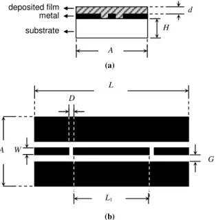
The resonators were fabricated on Piconics® thin-film polished alumina substrate (εr = 9.8, tanδ = 0.0001), using a conventional photolithography process. Schematics and physical parameters of the considered resonators are shown in Fig. 1. The cross-section of the resonators can be observed in Fig. 1 (a). The height and width of the alumina substrate are respectively H = 635 µm and A = 5.0 mm. The thickness d of the film is measured above the circuit gold metallization. According to the top view of the resonator, depicted in Fig. 1 (b), the total length of the circuit is L = 25.4 mm, while the length of the resonator middle-section is L1 = 15.3 mm and the coupling gap is D = 100 µm. Further, the width of the CPW central line and lateral gap are respectively W = 500 µm and
G = 210 µm.
(a)
(b)
Figure 1. Schematics and parameters of the resonators. (a) cross-section, and (b) top view.
All films used in this work were prepared by the screen printed method with double deposition layer over the prepared CPW resonators. After the deposition of the first layer, the films were heated at a rate of 1°C/min from environment temperature to 400°C. Afterwards, the temperature was raised from 400°C to 900°C at a rate of 5°C/min. Once the film had cooled down to room temperature, a second layer was screen-printed over the first one. The same thermal treatment was performed for the second deposited layer. The film thickness (d) was measured with a precision micrometer. The obtained films and their measured thickness are presented in Table I.
B. Microwave measurements
The fundamental resonance peak of each film-coated resonator was measured using a vector network analyzer (HP 8720C; 50 MHz ~ 20 GHz). Fig. 2 shows the experimental insertion loss peaks obtained for the film-coated resonators (S21 parameter) in comparison with a reference CPW resonator (with the same physical dimensions but without film coating).
TABLE I. COMPOSITION AND THICKNESS OF THE DEPOSITED FILMS.
Measured Thickness Film Composition
d (µµµµm)
MTO 113
MTO(0.95)–CTO(0.05) 165
MTO(0.50)–CTO(0.50) 120
MTO(0.20)–CTO(0.80) 135
CTO 105
Figure 2. Measured fundamental resonance peaks for the analyzed resonators.
As can be seen from this figure, starting with pure MTO and increasing the CTO concentrations, a downshift of resonance peaks is observed.
As mentioned previously, having measured the fundamental resonance frequency peak and since the thickness of the film is known, the relative dielectric constant of the ceramic material constituent of the film can be obtained from interpolation in the set of theoretical (simulated) curves, shown in Fig. 3. These curves of fundamental resonance peak as a function of the relative dielectric constant were obtained from the results of multiple simulations of CPW resonators for films with different dielectric constant and thickness using a commercially available microwave-frequency structure simulator – CST Microwave Studio®.
To refine the value of the relative dielectric constant obtained from interpolation, an optimization of the structure simulation was carried out. By making fine adjustments in the
W
D
G
L1
L
A
metal
substrate deposited film
H
A
d
relative dielectric constant, it was possible to find the value for the best match between theoretical and experimental results. This optimization procedure was carried out for each fabricated film. As an example, Fig. 4 shows the measured and simulated insertion loss for the resonator with MTO(0.2)–CTO(0.8). It can be observed that both results are in very good agreement.
The highest dielectric constant value measured was 17.5 for the CTO film and the lowest one was 4.2 for the MTO film. A strong relationship between the film relative dielectric constant and the concentration of CTO (or alternatively MTO) in the composite was observed. Fig. 5 displays the measured values for the dielectric constant according to the relative concentrations of CTO and MTO. An exponential fitting was applied to these data and the resulting curve is depicted also in Fig. 5, laying emphasis on this relationship. This characteristic could be used as a guide to formulate a particular material with a specific dielectric constant at some given frequency.
The film loss at a given resonance frequency can be determined from the insertion loss and loaded quality factor QL
of the measured resonance peak. The value of QL is extracted
from the S21 parameter measurement by means of the expression:
QL = fR /∆f3dB (1)
where fR is the peak frequency and ∆f3dB is the 3 dB bandwidth of the resonance peak. The unloaded quality factor Q0 can be calculated from [13]:
( )
( )
( )20
0 21
10 1
R
f S
R L R
f Q f
Q
−
= (2)
Finally, the dielectric loss can be calculated with the following approximate expression:
0
1 tan
Q
≈
δ (3)
Expression (3) is used assuming that dielectric losses are considerably higher than conductor and radiation losses [14]. The results found for dielectric loss tangent of the films remained between 0.0064 and 0.0098, for frequencies in the range from 3.22 to 3.89 GHz. The dielectric properties of the films analyzed in this work are summarized in Table II. These values are proximate to the measuring sensibility of the method, considering the dimensions of the resonator used, indicating that the actual values of film loss are probably lower than the ones observed.
The quality factor of ceramic films can be improved by means of a diversity of methods. Doping MTO with niobium increases the dielectric constant and helps eliminate defects [15]. Annealing process and the use of complex layered structures of MTO-CTO are other techniques to improve the dielectric properties of ceramic films [16, 17]. The list of variations that can be tentatively applied in the fabrication
processes in order to obtain materials with higher dielectric constant and lower losses is extensive.
TABLE II. EXPERIMENTAL RESULTS FOR THE DEPOSITED FILMS.
Film Composition Fundamental peak
frequency (GHz) r tan
MTO 3.89 4.2 0.0064
MTO(0.95)–CTO(0.05) 3.88 5.1 0.0082
MTO(0.50)–CTO(0.50) 3.66 8.3 0.0066
MTO(0.20)–CTO(0.80) 3.38 12.4 0.0090
CTO 3.22 17.5 0.0090
Figure 3. Theoretical prediction for the relationship between the fundamental resonance frequency and the film relative dielectric constant for
different thickness (d in µm) for the dimensions of the elaborated CPW resonators.
Figure 4. Measured and simulated insertion loss for the resonator with MTO(0.2)–CTO(0.8).
Figure 5. Relationship between the film relative dielectric constant and the concentration of CTO.
III. CONCLUSIONS
Dielectric constant and losses of MTO, CTO and MTO(x)–
CTO(1-x) composite screen-printed thick films at room temperature were measured for the first time in the microwave frequency range using the CPW resonator method. Experimental results are in a very good agreement with theoretical analysis. The highest dielectric constant value measured was 17.5 for the CTO film and the lowest one was 4.2 for the MTO film; the dielectric loss tangent of the films observed was between 0.0064 and 0.0098, for frequencies in the range from 3.22 to 3.89 GHz. A strong dependence of the
dielectric constant with the MTO-CTO composite
concentrations in the films was observed and can be eventually used as a method to elaborate some material with a determinate dielectric constant value at a specific frequency.
ACKNOWLEDGMENT
This work was supported by Conselho Nacional de Desenvolvimento Científico e Tecnológico (CNPq), the Fundação Carlos Chagas Filho de Amparo à Pesquisa do Estado do Rio de Janeiro (FAPERJ) and the Fundação Cearense de Apoio ao Desenvolvimento Científico e Tecnológico (FUNCAP), Brazil.
The ceramic films were fabricated by the group of Dr. A. S. B. Sombra, Department of Physics, UFC, Brazil. The resonators were printed by photolithography at LabSem (Semiconductor Laboratory), PUC-Rio, Brazil. All microwave measurements were carried out at CETUC/PUC-Rio, Brazil.
The authors acknowledge the use of FDTD software CST Microwave Studio® under the CST Cooperation License
Agreement with CETUC/PUC-Rio. All simulations of the microwave structures (resonators) presented in this work were carried out in this platform.
REFERENCES
[1] S. J. Fiedziuszko, and others, “Dielectric Materials, Devices, and Circuits,” IEEE Transactions on Microwave Theory and Techniques, vol. 50, no. 3, pp. 706-720, March 2002.
[2] D. Iddles, and I. M. Reaneyw, “Microwave dielectric ceramics for resonators and filters in mobile phone networks,” J. Am. Ceram. Soc., vol. 89, no. 7, pp. 2063–2072, 2006.
[3] C-L. Huang, and M-H Weng, “Improved high Q value of MgTiO3– CaTiO3 microwave dielectric ceramics at low sintering temperature,” Materials Research Bulletin 36, pp. 2741–2750, 2001.
[4] K. Wakino, “Recent development of dielectric resonator materials and filters in Japan,” Ferroelectrics, vol. 91, no. 1, pp. 69 – 86, 1989. [5] B. D. Lee, K. H. Yoon, E. S. Kim, and T. H. Kim, “Microwave
dielectric properties of CaTiO3 and MgTiO3 thin films,” Jpn. J. Appl. Phys., vol. 42, pp. 6158–6161, 2003.
[6] X. M. Chen, L. Li, and X. Q. Liu, “Layered complex structures of MgTiO3 and CaTiO3 dielectric ceramics,” Materials Science and Engineering B99, pp. 255–258, 2003.
[7] L. Li, X. M. Chen, and X. C. Fan, “Characterization of MgTiO3– CaTiO3-layered microwave dielectric resonators with TE01δ mode,” J. Am. Ceram. Soc., vol. 89, no. 2, pp. 557–561, 2006.
[8] M. R. P. Santos, M. A. S. Silva, A. S. B. Sombra, and F. N. A. Freire, “Síntese e estudo das propriedades dielétricas dos compósitos [x]CaTiO3-[1-x]MgTiO3. In: XXVI Encontro de Físicos do Norte e Nordeste, 2008, Recife-PE, Brazil. Proc. of XXVI Encontro de Físicos do Norte e Nordeste, ID: 774-1, 2008.
[9] Q. Zhang, and P. J. McGinn, “Characterization of calcium titanate eutectic by scanning microwave microscopy,” J. Am. Ceram. Soc., vol. 89, no. 12, pp. 3817-3823, 2006.
[10] S. H. Shim, et al., “Microwave Characteristics of MgTiO3–CaTiO3 Dielectric Ceramics Fabricated Using Spark Plasma Sintering, ” Jpn. J. Appl. Phys. vol. 44, no. 7A, pp. 5073-5075, 2005.
[11] P. M. Suherman, T. J. Jackson and M. J. Lancaster. “Comparison of Techniques for Microwave Characterization of BST Thin Films, ” IEEE Transactions on Microwave Theory and Techniques, vol. 55, no. 2, pp. 397-401, February 2007.
[12] L. S. Demenicis, R. A. A. Lima, L. F. M. Conrado, W. Margulis and M. C. R. Carvalho, “A CPW linear resonator method for the microwave characterization of high dielectric constant films,” Microwave and Opt Technol Lett, vol. 49, no. 3, March 2007.
[13] R. E. Collin, Foundations for Microwave Engineering , 2nd edition. Hoboken, NJ: Wiley-IEEE Press, 2001.
[14] K. C. Gupta, R. Garg, I. J. Bahl, and P. Bhartia, Microstrip Lines and Slotlines, 2nd edition. Norwood, MA: Artech, 1996.
[15] V. M. Ferreira, and J. L. Baptista, “Role of niobium in magnesium titanate microwave dielectric ceramics,” J. Am. Ceram. Soc., vol. 79, no. 6, pp. 1697-1698, 2006.
[16] B. D. Lee, H. R. Lee, and K. H. Yoon, “Effect of stacking layers on the microwave dielectric properties of MgTiO3–CaTiO3 multilayered thin films,” J. Am. Ceram. Soc., vol. 88, no. 5, pp. 1197-1200, 2005. [17] L. Li, X. M. Chen, and X. C. Fan, “Microwave Dielectric Properties of
MgTiO3–CaTiO3 Dielectric Ceramics,” J. Eur. Ceram. Soc., vol. 26, pp. 2817-2821, 2006.