Data Sheet
Information contained in this publication regarding device applications and the like is provided only for your convenience and may be superseded by updates. It is your responsibility to ensure that your application meets with your specifications. MICROCHIP MAKES NO REPRESENTATIONS OR WARRANTIES OF ANY KIND WHETHER EXPRESS OR IMPLIED, WRITTEN OR ORAL, STATUTORY OR OTHERWISE, RELATED TO THE INFORMATION, INCLUDING BUT NOT LIMITED TO ITS CONDITION, QUALITY, PERFORMANCE, MERCHANTABILITY OR FITNESS FOR PURPOSE. Microchip disclaims all liability arising from this information and its use. Use of Microchip devices in life support and/or safety applications is entirely at the buyer’s risk, and the buyer agrees to defend, indemnify and hold harmless Microchip from any and all damages, claims, suits, or expenses resulting from such use. No licenses are conveyed, implicitly or otherwise, under any Microchip intellectual property rights.
Trademarks
The Microchip name and logo, the Microchip logo, dsPIC, KEELOQ, KEELOQ logo, MPLAB, PIC, PICmicro, PICSTART, rfPIC and UNI/O are registered trademarks of Microchip Technology Incorporated in the U.S.A. and other countries. FilterLab, Hampshire, HI-TECH C, Linear Active Thermistor, MXDEV, MXLAB, SEEVAL and The Embedded Control Solutions Company are registered trademarks of Microchip Technology Incorporated in the U.S.A.
Analog-for-the-Digital Age, Application Maestro, CodeGuard, dsPICDEM, dsPICDEM.net, dsPICworks, dsSPEAK, ECAN, ECONOMONITOR, FanSense, HI-TIDE, In-Circuit Serial Programming, ICSP, Mindi, MiWi, MPASM, MPLAB Certified logo, MPLIB, MPLINK, mTouch, Octopus, Omniscient Code Generation, PICC, PICC-18, PICDEM, PICDEM.net, PICkit, PICtail, PIC32 logo, REAL ICE, rfLAB, Select Mode, Total Endurance, TSHARC, UniWinDriver, WiperLock and ZENA are trademarks of Microchip Technology Incorporated in the U.S.A. and other countries.
SQTP is a service mark of Microchip Technology Incorporated in the U.S.A.
All other trademarks mentioned herein are property of their respective companies.
© 2009, Microchip Technology Incorporated, Printed in the U.S.A., All Rights Reserved.
Printed on recycled paper. intended manner and under normal conditions.
• There are dishonest and possibly illegal methods used to breach the code protection feature. All of these methods, to our knowledge, require using the Microchip products in a manner outside the operating specifications contained in Microchip’s Data Sheets. Most likely, the person doing so is engaged in theft of intellectual property.
• Microchip is willing to work with the customer who is concerned about the integrity of their code.
• Neither Microchip nor any other semiconductor manufacturer can guarantee the security of their code. Code protection does not mean that we are guaranteeing the product as “unbreakable.”
Code protection is constantly evolving. We at Microchip are committed to continuously improving the code protection features of our products. Attempts to break Microchip’s code protection feature may be a violation of the Digital Millennium Copyright Act. If such acts allow unauthorized access to your software or other copyrighted work, you may have a right to sue for relief under that Act.
Microchip received ISO/TS-16949:2002 certification for its worldwide headquarters, design and wafer fabrication facilities in Chandler and Tempe, Arizona; Gresham, Oregon and design centers in California and India. The Company’s quality system processes and procedures are for its PIC®MCUs and dsPIC® DSCs, KEELOQ®code hopping
Universal Serial Bus Features:
• USB V2.0 Compliant• Low Speed (1.5 Mb/s) and Full Speed (12 Mb/s) • Supports Control, Interrupt, Isochronous and Bulk
Transfers
• Supports up to 32 Endpoints (16 bidirectional) • 1 Kbyte Dual Access RAM for USB
• On-Chip USB Transceiver with On-Chip Voltage Regulator
• Interface for Off-Chip USB Transceiver
• Streaming Parallel Port (SPP) for USB streaming transfers (40/44-pin devices only)
Power-Managed Modes:
• Run: CPU on, Peripherals on • Idle: CPU off, Peripherals on • Sleep: CPU off, Peripherals off• Idle mode Currents Down to 5.8 μA Typical • Sleep mode Currents Down to 0.1 μA Typical • Timer1 Oscillator: 1.1 μA Typical, 32 kHz, 2V • Watchdog Timer: 2.1 μA Typical
• Two-Speed Oscillator Start-up
Flexible Oscillator Structure:
• Four Crystal modes, including High-Precision PLL for USB
• Two External Clock modes, Up to 48 MHz • Internal Oscillator Block:
- 8 user-selectable frequencies, from 31 kHz to 8 MHz
- User-tunable to compensate for frequency drift • Secondary Oscillator using Timer1 @ 32 kHz • Dual Oscillator Options allow Microcontroller and
USB module to Run at Different Clock Speeds • Fail-Safe Clock Monitor:
- Allows for safe shutdown if any clock stops
Peripheral Highlights:
• High-Current Sink/Source: 25 mA/25 mA • Three External Interrupts
• Four Timer modules (Timer0 to Timer3)
• Up to 2 Capture/Compare/PWM (CCP) modules: - Capture is 16-bit, max. resolution 5.2 ns (TCY/16) - Compare is 16-bit, max. resolution 83.3 ns (TCY) - PWM output: PWM resolution is 1 to 10-bit • Enhanced Capture/Compare/PWM (ECCP) module:
- Multiple output modes - Selectable polarity - Programmable dead time - Auto-shutdown and auto-restart • Enhanced USART module:
- LIN bus support
• Master Synchronous Serial Port (MSSP) module Supporting 3-Wire SPI (all 4 modes) and I2C™ Master and Slave modes
• 10-Bit, Up to 13-Channel Analog-to-Digital Converter (A/D) module with Programmable Acquisition Time • Dual Analog Comparators with Input Multiplexing
Special Microcontroller Features:
• C Compiler Optimized Architecture with OptionalExtended Instruction Set
• 100,000 Erase/Write Cycle Enhanced Flash Program Memory Typical
• 1,000,000 Erase/Write Cycle Data EEPROM Memory Typical
• Flash/Data EEPROM Retention: > 40 Years • Self-Programmable under Software Control • Priority Levels for Interrupts
• 8 x 8 Single-Cycle Hardware Multiplier • Extended Watchdog Timer (WDT):
- Programmable period from 41 ms to 131s • Programmable Code Protection
• Single-Supply 5V In-Circuit Serial Programming™ (ICSP™) via Two Pins • In-Circuit Debug (ICD) via Two Pins
• Optional Dedicated ICD/ICSP Port (44-pin, TQFP package only)
• Wide Operating Voltage Range (2.0V to 5.5V)
Device
Program Memory Data Memory
I/O 10-Bit A/D (ch)
CCP/ECCP (PWM) SPP
MSSP
SA
R
T
ar
at
or
s
Timers 8/16-Bit Flash # Single-Word SRAM EEPROM
SPI Master
Pin Diagrams
40-Pin PDIP PIC18 F 24 5528-Pin PDIP, SOIC
PIC18 F 25 50 10 11 2 3 4 5 6 1 8 7 9 12 13 14 15 16 17 18 19 20 23 24 25 26 27 28 22 21
MCLR/VPP/RE3
RA0/AN0 RA1/AN1
RA2/AN2/VREF-/CVREF
RA3/AN3/VREF+
RA4/T0CKI/C1OUT/RCV RA5/AN4/SS/HLVDIN/C2OUT VSS OSC1/CLKI OSC2/CLKO/RA6 RC0/T1OSO/T13CKI
RC1/T1OSI/CCP2(1)/UOE
RC2/CCP1 VUSB RB7/KBI3/PGD RB6/KBI2/PGC RB5/KBI1/PGM RB4/AN11/KBI0
RB3/AN9/CCP2(1)/VPO
RB2/AN8/INT2/VMO RB1/AN10/INT1/SCK/SCL RB0/AN12/INT0/FLT0/SDI/SDA VDD VSS RC7/RX/DT/SDO RC6/TX/CK RC5/D+/VP RC4/D-/VM RB7/KBI3/PGD RB6/KBI2/PGC RB5/KBI1/PGM RB4/AN11/KBI0/CSSPP
RB3/AN9/CCP2(1)/VPO
RB2/AN8/INT2/VMO RB1/AN10/INT1/SCK/SCL RB0/AN12/INT0/FLT0/SDI/SDA VDD VSS RD7/SPP7/P1D RD6/SPP6/P1C RD5/SPP5/P1B RD4/SPP4 RC7/RX/DT/SDO RC6/TX/CK RC5/D+/VP RC4/D-/VM RD3/SPP3 RD2/SPP2
MCLR/VPP/RE3
RA0/AN0 RA1/AN1
RA2/AN2/VREF-/CVREF
RA3/AN3/VREF+
RA4/T0CKI/C1OUT/RCV RA5/AN4/SS/HLVDIN/C2OUT RE0/AN5/CK1SPP RE1/AN6/CK2SPP RE2/AN7/OESPP VDD VSS OSC1/CLKI OSC2/CLKO/RA6 RC0/T1OSO/T13CKI
RC1/T1OSI/CCP2(1)/UOE
RC2/CCP1/P1A VUSB RD0/SPP0 RD1/SPP1 1 2 3 4 5 6 7 8 9 10 11 12 13 14 15 16 17 18 19 20 40 39 38 37 36 35 34 33 32 31 30 29 28 27 26 25 24 23 22 21 PI C 1 8F4 455 PI C 1 8F4 550
Pin Diagrams (Continued)
PIC18F4455 44-Pin TQFP 44-Pin QFN PIC18F4455 PIC18F4550 PIC18F4550 10 11 2 3 6 118 19 20 21 22 12 13 14 15
38
8 7
44 43 42 41 40 39
16 17 29 30 31 32 33 23 24 25 26 27 28 36 35 34
9 37 RA3 /AN3 /V RE F + RA2 /AN 2 /V RE F -/C V RE F RA1 /AN1 RA0 /AN0 MC LR /V PP /RE 3 NC/ ICCK (2 )/ICP G C (2 ) RB 7/ K B I3 /P GD RB 6/ K B I2 /P GC RB 5 /KBI 1 /P G M RB4 /AN1 1 /K B I0 /C SSPP NC/ICDT (2 )/ICP G D (2 ) RC6 /T X /CK RC5 /D+/VP RC4 /D-/V M RD3 /SPP3 RD2 /SPP2 RD1 /SPP1 RD0 /SPP0 V US B RC2 /CCP1 /P1 A RC1 /T 1 O SI/CCP 2 (1 )/U O E NC/ ICPOR T S (2 )
NC/ICRST(2)/ICVPP(2)
RC0/T1OSO/T13CKI OSC2/CLKO/RA6 OSC1/CLKI VSS VDD RE2/AN7/OESPP RE1/AN6/CK2SPP RE0/AN5/CK1SPP RA5/AN4/SS/HLVDIN/C2OUT RA4/T0CKI/C1OUT/RCV RC7/RX/DT/SDO RD4/SPP4 RD5/SPP5/P1B RD6/SPP6/P1C VSS VDD RB0/AN12/INT0/FLT0/SDI/SDA RB1/AN10/INT1/SCK/SCL RB2/AN8/INT2/VMO
RB3/AN9/CCP2(1)/VPO
RD7/SPP7/P1D 5 4 10 11 2 3 6 1
18 19 20 21 22 12 13 14 15
38
8 7
44 43 42 41 40 39
16 17 29 30 31 32 33 23 24 25 26 27 28 36 35 34
9 37 3 /AN3 /V RE F + 2/V RE F -/C V RE F RA1 /AN1 RA0 /AN0 L R /V PP /RE 3 7 /K B I3 /P GD 6 /K B I2 /P GC /KBI 1 /PG M 1 /KBI 0 /CS SPP NC RC6 /T X/CK RC5 /D +/VP RC4 /D -/ VM RD3 /SPP3 RD2 /SPP2 RD1 /SPP1 RD0 /SPP0 V US B RC2 /C CP 1 /P1 A RC1 /T 1 O S I/CCP2 (1 )/UOE RC0 /T 1 O SO/T 1 3 CKI OSC2/CLKO/RA6 OSC1/CLKI VSS VDD RE2/AN7/OESPP RE1/AN6/CK2SPP RE0/AN5/CK1SPP RA5/AN4/SS/HLVDIN/C2OUT RA4/T0CKI/C1OUT/RCV RC7/RX/DT/SDO RD4/SPP4 RD5/SPP5/P1B RD6/SPP6/P1C VSS VDD RB0/AN12/INT0/FLT0/SDI/SDA RB1/AN10/INT1/SCK/SCL RB2/AN8/INT2/VMO C P 2 (1 )/V P O RD7/SPP7/P1D 5
4 VSS
VDD
Table of Contents
1.0 Device Overview ... 7
2.0 Oscillator Configurations ... 23
3.0 Power-Managed Modes ... 35
4.0 Reset ... 45
5.0 Memory Organization ... 59
6.0 Flash Program Memory ... 81
7.0 Data EEPROM Memory ... 91
8.0 8 x 8 Hardware Multiplier... 97
9.0 Interrupts ... 99
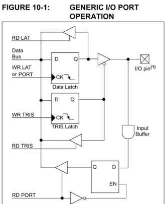
10.0 I/O Ports ... 113
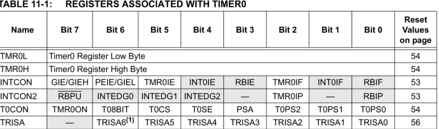
11.0 Timer0 Module ... 127
12.0 Timer1 Module ... 131
13.0 Timer2 Module ... 137
14.0 Timer3 Module ... 139
15.0 Capture/Compare/PWM (CCP) Modules ... 143
16.0 Enhanced Capture/Compare/PWM (ECCP) Module... 151
17.0 Universal Serial Bus (USB) ... 165
18.0 Streaming Parallel Port ... 191
19.0 Master Synchronous Serial Port (MSSP) Module ... 197
20.0 Enhanced Universal Synchronous Asynchronous Receiver Transmitter (EUSART) ... 243
21.0 10-Bit Analog-to-Digital Converter (A/D) Module ... 265
22.0 Comparator Module... 275
23.0 Comparator Voltage Reference Module ... 281
24.0 High/Low-Voltage Detect (HLVD)... 285
25.0 Special Features of the CPU ... 291
26.0 Instruction Set Summary ... 313
27.0 Development Support... 363
28.0 Electrical Characteristics ... 367
29.0 DC and AC Characteristics Graphs and Tables ... 407
30.0 Packaging Information... 409
Appendix A: Revision History... 419
Appendix B: Device Differences... 419
Appendix C: Conversion Considerations ... 420
Appendix D: Migration From Baseline to Enhanced Devices... 420
Appendix E: Migration From Mid-Range to Enhanced Devices ... 421
Appendix F: Migration From High-End to Enhanced Devices... 421
Index ... 423
The Microchip Web Site ... 433
Customer Change Notification Service ... 433
Customer Support ... 433
Reader Response ... 434
TO OUR VALUED CUSTOMERS
It is our intention to provide our valued customers with the best documentation possible to ensure successful use of your Microchip products. To this end, we will continue to improve our publications to better suit your needs. Our publications will be refined and enhanced as new volumes and updates are introduced.
If you have any questions or comments regarding this publication, please contact the Marketing Communications Department via E-mail at [email protected] or fax the Reader Response Form in the back of this data sheet to (480) 792-4150. We welcome your feedback.
Most Current Data Sheet
To obtain the most up-to-date version of this data sheet, please register at our Worldwide Web site at: http://www.microchip.com
You can determine the version of a data sheet by examining its literature number found on the bottom outside corner of any page. The last character of the literature number is the version number, (e.g., DS30000A is version A of document DS30000).
Errata
An errata sheet, describing minor operational differences from the data sheet and recommended workarounds, may exist for current devices. As device/documentation issues become known to us, we will publish an errata sheet. The errata will specify the revision of silicon and revision of document to which it applies.
To determine if an errata sheet exists for a particular device, please check with one of the following: • Microchip’s Worldwide Web site; http://www.microchip.com
• Your local Microchip sales office (see last page)
When contacting a sales office, please specify which device, revision of silicon and data sheet (include literature number) you are using.
Customer Notification System
1.0
DEVICE OVERVIEW
This document contains device-specific information for the following devices:
This family of devices offers the advantages of all PIC18 microcontrollers – namely, high computational performance at an economical price – with the addition of high-endurance, Enhanced Flash program memory. In addition to these features, the PIC18F2455/2550/4455/4550 family introduces design enhancements that make these microcontrollers a log-ical choice for many high-performance, power sensitive applications.
1.1
New Core Features
1.1.1 nanoWatt TECHNOLOGY
All of the devices in the PIC18F2455/2550/4455/4550 family incorporate a range of features that can signifi-cantly reduce power consumption during operation. Key items include:
• Alternate Run Modes: By clocking the controller from the Timer1 source or the internal oscillator block, power consumption during code execution can be reduced by as much as 90%.
• Multiple Idle Modes: The controller can also run with its CPU core disabled but the peripherals still active. In these states, power consumption can be reduced even further, to as little as 4%, of normal operation requirements.
• On-the-Fly Mode Switching: The
power-managed modes are invoked by user code during operation, allowing the user to incorporate power-saving ideas into their application’s software design.
• Low Consumption in Key Modules: The power requirements for both Timer1 and the Watchdog Timer are minimized. See Section 28.0
“Electrical Characteristics” for values.
1.1.2 UNIVERSAL SERIAL BUS (USB)
Devices in the PIC18F2455/2550/4455/4550 family incorporate a fully featured Universal Serial Bus communications module that is compliant with the USB Specification Revision 2.0. The module supports both low-speed and full-speed communication for all sup-ported data transfer types. It also incorporates its own
1.1.3 MULTIPLE OSCILLATOR OPTIONS
AND FEATURES
All of the devices in the PIC18F2455/2550/4455/4550 family offer twelve different oscillator options, allowing users a wide range of choices in developing application hardware. These include:
• Four Crystal modes using crystals or ceramic resonators.
• Four External Clock modes, offering the option of using two pins (oscillator input and a divide-by-4 clock output) or one pin (oscillator input, with the second pin reassigned as general I/O).
• An internal oscillator block which provides an 8 MHz clock (±2% accuracy) and an INTRC source (approximately 31 kHz, stable over temperature and VDD), as well as a range of 6 user-selectable clock frequencies, between 125 kHz to 4 MHz, for a total of 8 clock
frequencies. This option frees an oscillator pin for use as an additional general purpose I/O. • A Phase Lock Loop (PLL) frequency multiplier,
available to both the High-Speed Crystal and External Oscillator modes, which allows a wide range of clock speeds from 4 MHz to 48 MHz. • Asynchronous dual clock operation, allowing the
USB module to run from a high-frequency oscillator while the rest of the microcontroller is clocked from an internal low-power oscillator.
Besides its availability as a clock source, the internal oscillator block provides a stable reference source that gives the family additional features for robust operation:
• Fail-Safe Clock Monitor: This option constantly monitors the main clock source against a reference signal provided by the internal
oscillator. If a clock failure occurs, the controller is switched to the internal oscillator block, allowing for continued low-speed operation or a safe application shutdown.
• Two-Speed Start-up: This option allows the internal oscillator to serve as the clock source from Power-on Reset, or wake-up from Sleep mode, until the primary clock source is available.
• PIC18F2455 • PIC18LF2455
• PIC18F2550 • PIC18LF2550
• PIC18F4455 • PIC18LF4455
1.2
Other Special Features
• Memory Endurance: The Enhanced Flash cells for both program memory and data EEPROM are rated to last for many thousands of erase/write cycles – up to 100,000 for program memory and 1,000,000 for EEPROM. Data retention without refresh is conservatively estimated to be greater than 40 years.
• Self-Programmability: These devices can write to their own program memory spaces under internal software control. By using a bootloader routine, located in the protected Boot Block at the top of program memory, it becomes possible to create an application that can update itself in the field. • Extended Instruction Set: The
PIC18F2455/2550/4455/4550 family introduces an optional extension to the PIC18 instruction set, which adds 8 new instructions and an Indexed Literal Offset Addressing mode. This extension, enabled as a device configuration option, has been specifically designed to optimize re-entrant application code originally developed in high-level languages such as C.
• Enhanced CCP Module: In PWM mode, this module provides 1, 2 or 4 modulated outputs for controlling half-bridge and full-bridge drivers. Other features include auto-shutdown for disabling PWM outputs on interrupt or other select conditions, and auto-restart to reactivate outputs once the condition has cleared.
• Enhanced Addressable USART: This serial communication module is capable of standard RS-232 operation and provides support for the LIN bus protocol. The TX/CK and RX/DT signals can be inverted, eliminating the need for inverting buffers. Other enhancements include Automatic Baud Rate Detection and a 16-bit Baud Rate Generator for improved resolution. When the microcontroller is using the internal oscillator block, the EUSART provides stable operation for applications that talk to the outside world without using an external crystal (or its accompanying power requirement).
• 10-Bit A/D Converter: This module incorporates programmable acquisition time, allowing for a channel to be selected and a conversion to be initiated, without waiting for a sampling period and thus, reducing code overhead.
• Dedicated ICD/ICSP Port: These devices introduce the use of debugger and programming pins that are not multiplexed with other micro-controller features. Offered as an option in select packages, this feature allows users to develop I/O intensive applications while retaining the ability to program and debug in the circuit.
1.3
Details on Individual Family
Members
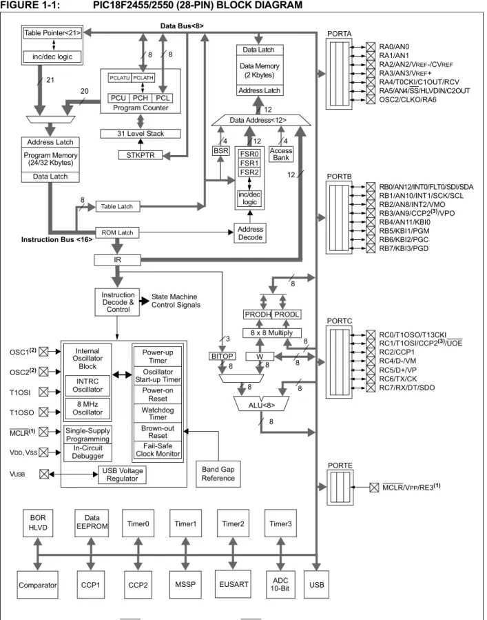
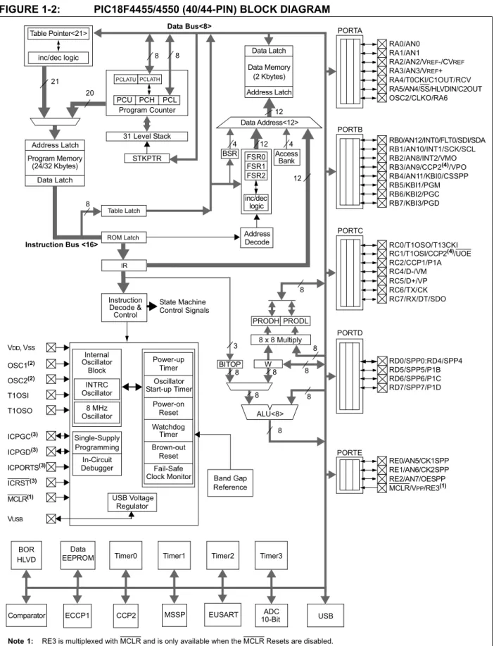
Devices in the PIC18F2455/2550/4455/4550 family are available in 28-pin and 40/44-pin packages. Block diagrams for the two groups are shown in Figure 1-1 and Figure 1-2.
The devices are differentiated from each other in six ways:
1. Flash program memory (24 Kbytes for PIC18FX455 devices, 32 Kbytes for PIC18FX550 devices).
2. A/D channels (10 for 28-pin devices, 13 for 40/44-pin devices).
3. I/O ports (3 bidirectional ports and 1 input only port on 28-pin devices, 5 bidirectional ports on 40/44-pin devices).
4. CCP and Enhanced CCP implementation (28-pin devices have two standard CCP modules, 40/44-pin devices have one standard CCP module and one ECCP module).
5. Streaming Parallel Port (present only on 40/44-pin devices).
All other features for devices in this family are identical. These are summarized in Table 1-1.
The pinouts for all devices are listed in Table 1-2 and Table 1-3.
TABLE 1-1: DEVICE FEATURES
Features PIC18F2455 PIC18F2550 PIC18F4455 PIC18F4550
Operating Frequency DC – 48 MHz DC – 48 MHz DC – 48 MHz DC – 48 MHz
Program Memory (Bytes) 24576 32768 24576 32768
Program Memory (Instructions) 12288 16384 12288 16384
Data Memory (Bytes) 2048 2048 2048 2048
Data EEPROM Memory (Bytes) 256 256 256 256
Interrupt Sources 19 19 20 20
I/O Ports Ports A, B, C, (E) Ports A, B, C, (E) Ports A, B, C, D, E Ports A, B, C, D, E
Timers 4 4 4 4
Capture/Compare/PWM Modules 2 2 1 1
Enhanced Capture/ Compare/PWM Modules
0 0 1 1
Serial Communications MSSP,
Enhanced USART
MSSP, Enhanced USART
MSSP, Enhanced USART
MSSP, Enhanced USART Universal Serial Bus (USB)
Module
1 1 1 1
Streaming Parallel Port (SPP) No No Yes Yes
10-Bit Analog-to-Digital Module 10 Input Channels 10 Input Channels 13 Input Channels 13 Input Channels
Comparators 2 2 2 2
Resets (and Delays) POR, BOR,
RESET Instruction,
Stack Full, Stack Underflow
(PWRT, OST), MCLR (optional),
WDT
POR, BOR,
RESET Instruction,
Stack Full, Stack Underflow
(PWRT, OST), MCLR (optional),
WDT
POR, BOR,
RESET Instruction,
Stack Full, Stack Underflow
(PWRT, OST), MCLR (optional),
WDT
POR, BOR,
RESET Instruction,
Stack Full, Stack Underflow
(PWRT, OST), MCLR (optional),
WDT Programmable Low-Voltage
Detect
Yes Yes Yes Yes
Programmable Brown-out Reset Yes Yes Yes Yes
Instruction Set 75 Instructions;
83 with Extended Instruction Set
enabled
75 Instructions; 83 with Extended
Instruction Set enabled
75 Instructions; 83 with Extended
Instruction Set enabled
75 Instructions; 83 with Extended
Instruction Set enabled
Packages 28-Pin PDIP
28-Pin SOIC
28-Pin PDIP 28-Pin SOIC
40-Pin PDIP 44-Pin QFN 44-Pin TQFP
FIGURE 1-1: PIC18F2455/2550 (28-PIN) BLOCK DIAGRAM Data Latch Data Memory (2 Kbytes) Address Latch Data Address<12> 12 Access BSR 4 4
PCH PCL
PCLATH
8
31 Level Stack Program Counter
PRODL PRODH
8 x 8 Multiply
8 8 8 ALU<8> Address Latch Program Memory (24/32 Kbytes) Data Latch 20 8 8 Table Pointer<21> inc/dec logic 21 8 Data Bus<8> Table Latch 8 IR 12 3 ROM Latch PCLATU PCU PORTE
MCLR/VPP/RE3(1)
Note 1: RE3 is multiplexed with MCLR and is only available when the MCLR Resets are disabled.
2: OSC1/CLKI and OSC2/CLKO are only available in select oscillator modes and when these pins are not being used as digital I/O. Refer
to Section 2.0 “Oscillator Configurations” for additional information.
3: RB3 is the alternate pin for CCP2 multiplexing.
W
Instruction Bus <16>
STKPTR Bank 8 8 8 BITOP FSR0 FSR1 FSR2 inc/dec Address 12 Decode logic EUSART Comparator MSSP 10-Bit ADC Timer2 Timer1 Timer3 Timer0 HLVD CCP2 BOR Data EEPROM USB Instruction Decode & Control State Machine Control Signals Power-up Timer Oscillator Start-up Timer Power-on Reset Watchdog Timer OSC1(2) OSC2(2)
VDD,
Brown-out Reset Internal Oscillator Fail-Safe Clock Monitor Reference Band Gap VSS MCLR(1) Block INTRC Oscillator 8 MHz Oscillator Single-Supply Programming In-Circuit Debugger T1OSI T1OSO USB Voltage Regulator VUSB PORTB PORTC RB0/AN12/INT0/FLT0/SDI/SDA RC0/T1OSO/T13CKI
RC1/T1OSI/CCP2(3)/UOE
RC2/CCP1 RC4/D-/VM RC5/D+/VP RC6/TX/CK RC7/RX/DT/SDO RB1/AN10/INT1/SCK/SCL RB2/AN8/INT2/VMO
RB3/AN9/CCP2(3)/VPO
RB4/AN11/KBI0 RB5/KBI1/PGM RB6/KBI2/PGC RB7/KBI3/PGD PORTA RA4/T0CKI/C1OUT/RCV RA5/AN4/SS/HLVDIN/C2OUT
RA3/AN3/VREF+
RA2/AN2/VREF-/CVREF
RA1/AN1 RA0/AN0
OSC2/CLKO/RA6
FIGURE 1-2: PIC18F4455/4550 (40/44-PIN) BLOCK DIAGRAM Instruction Decode & Control Data Latch Data Memory (2 Kbytes) Address Latch Data Address<12> 12 Access BSR 4 4
PCH PCL
PCLATH
8
31 Level Stack Program Counter
PRODL PRODH
8 x 8 Multiply
8 BITOP 8 8 ALU<8> Address Latch Program Memory (24/32 Kbytes) Data Latch 20 8 8 Table Pointer<21> inc/dec logic 21 8 Data Bus<8> Table Latch 8 IR 12 3 ROM Latch PORTD RD0/SPP0:RD4/SPP4 PCLATU PCU PORTE
MCLR/VPP/RE3(1)
RE2/AN7/OESPP RE0/AN5/CK1SPP RE1/AN6/CK2SPP EUSART Comparator MSSP 10-Bit ADC Timer2 Timer1 Timer3 Timer0 CCP2 HLVD ECCP1 BOR Data EEPROM W
Instruction Bus <16>
STKPTR Bank 8 State Machine Control Signals 8 8 Power-up Timer Oscillator Start-up Timer Power-on Reset Watchdog Timer OSC1(2) OSC2(2)
VDD, VSS
Brown-out Reset Internal Oscillator Fail-Safe Clock Monitor Reference Band Gap MCLR(1) Block INTRC Oscillator 8 MHz Oscillator Single-Supply Programming In-Circuit Debugger T1OSI T1OSO RD5/SPP5/P1B RD6/SPP6/P1C RD7/SPP7/P1D PORTA PORTB PORTC RA4/T0CKI/C1OUT/RCV RA5/AN4/SS/HLVDIN/C2OUT RB0/AN12/INT0/FLT0/SDI/SDA RC0/T1OSO/T13CKI
RC1/T1OSI/CCP2(4)/UOE
RC2/CCP1/P1A RC4/D-/VM RC5/D+/VP RC6/TX/CK RC7/RX/DT/SDO
RA3/AN3/VREF+
RA2/AN2/VREF-/CVREF
RA1/AN1 RA0/AN0
RB1/AN10/INT1/SCK/SCL RB2/AN8/INT2/VMO
RB3/AN9/CCP2(4)/VPO
TABLE 1-2: PIC18F2455/2550 PINOUT I/O DESCRIPTIONS
Pin Name
Pin Number Pin
Type
Buffer
Type Description PDIP,
SOIC
MCLR/VPP/RE3 MCLR
VPP RE3
1 I
P I
ST
ST
Master Clear (input) or programming voltage (input). Master Clear (Reset) input. This pin is an active-low Reset to the device.
Programming voltage input. Digital input.
OSC1/CLKI OSC1 CLKI
9 I I
Analog Analog
Oscillator crystal or external clock input.
Oscillator crystal input or external clock source input. External clock source input. Always associated with pin function OSC1. (See OSC2/CLKO pin.)
OSC2/CLKO/RA6 OSC2
CLKO
RA6
10 O
O
I/O —
—
TTL
Oscillator crystal or clock output.
Oscillator crystal output. Connects to crystal or resonator in Crystal Oscillator mode.
In select modes, OSC2 pin outputs CLKO which has 1/4 the frequency of OSC1 and denotes the instruction cycle rate. General purpose I/O pin.
Legend: TTL = TTL compatible input CMOS = CMOS compatible input or output ST = Schmitt Trigger input with CMOS levels I = Input
O = Output P = Power
Note 1: Alternate assignment for CCP2 when CCP2MX Configuration bit is cleared.
PORTA is a bidirectional I/O port. RA0/AN0 RA0 AN0 2 I/O I TTL Analog Digital I/O. Analog input 0. RA1/AN1 RA1 AN1 3 I/O I TTL Analog Digital I/O. Analog input 1. RA2/AN2/VREF-/CVREF RA2 AN2 VREF-CVREF 4 I/O I I O TTL Analog Analog Analog Digital I/O. Analog input 2.
A/D reference voltage (low) input. Analog comparator reference output. RA3/AN3/VREF+ RA3 AN3 VREF+ 5 I/O I I TTL Analog Analog Digital I/O. Analog input 3.
A/D reference voltage (high) input. RA4/T0CKI/C1OUT/RCV RA4 T0CKI C1OUT RCV 6 I/O I O I ST ST — TTL Digital I/O.
Timer0 external clock input. Comparator 1 output.
External USB transceiver RCV input.
RA5/AN4/SS/ HLVDIN/C2OUT RA5 AN4 SS HLVDIN C2OUT 7 I/O I I I O TTL Analog TTL Analog — Digital I/O. Analog input 4. SPI slave select input.
High/Low-Voltage Detect input. Comparator 2 output.
RA6 — — — See the OSC2/CLKO/RA6 pin.
TABLE 1-2: PIC18F2455/2550 PINOUT I/O DESCRIPTIONS (CONTINUED)
Pin Name Pin Number Pin Type Buffer Type Description PDIP, SOIC
Legend: TTL = TTL compatible input CMOS = CMOS compatible input or output ST = Schmitt Trigger input with CMOS levels I = Input
O = Output P = Power
Note 1: Alternate assignment for CCP2 when CCP2MX Configuration bit is cleared.
PORTB is a bidirectional I/O port. PORTB can be software programmed for internal weak pull-ups on all inputs. RB0/AN12/INT0/FLT0/ SDI/SDA RB0 AN12 INT0 FLT0 SDI SDA 21 I/O I I I I I/O TTL Analog ST ST ST ST Digital I/O. Analog input 12. External interrupt 0.
PWM Fault input (CCP1 module). SPI data in.
I2C™ data I/O. RB1/AN10/INT1/SCK/ SCL RB1 AN10 INT1 SCK SCL 22 I/O I I I/O I/O TTL Analog ST ST ST Digital I/O. Analog input 10. External interrupt 1.
Synchronous serial clock input/output for SPI mode. Synchronous serial clock input/output for I2C mode. RB2/AN8/INT2/VMO RB2 AN8 INT2 VMO 23 I/O I I O TTL Analog ST — Digital I/O. Analog input 8. External interrupt 2.
External USB transceiver VMO output. RB3/AN9/CCP2/VPO RB3 AN9 CCP2(1) VPO 24 I/O I I/O O TTL Analog ST — Digital I/O. Analog input 9.
Capture 2 input/Compare 2 output/PWM2 output. External USB transceiver VPO output.
RB4/AN11/KBI0 RB4 AN11 KBI0 25 I/O I I TTL Analog TTL Digital I/O. Analog input 11. Interrupt-on-change pin. RB5/KBI1/PGM RB5 KBI1 PGM 26 I/O I I/O TTL TTL ST Digital I/O. Interrupt-on-change pin.
Low-Voltage ICSP™ Programming enable pin. RB6/KBI2/PGC RB6 KBI2 PGC 27 I/O I I/O TTL TTL ST Digital I/O. Interrupt-on-change pin.
In-Circuit Debugger and ICSP programming clock pin. RB7/KBI3/PGD RB7 KBI3 PGD 28 I/O I I/O TTL TTL ST Digital I/O. Interrupt-on-change pin.
In-Circuit Debugger and ICSP programming data pin. TABLE 1-2: PIC18F2455/2550 PINOUT I/O DESCRIPTIONS (CONTINUED)
Pin Name Pin Number Pin Type Buffer Type Description PDIP, SOIC
Legend: TTL = TTL compatible input CMOS = CMOS compatible input or output ST = Schmitt Trigger input with CMOS levels I = Input
O = Output P = Power
Note 1: Alternate assignment for CCP2 when CCP2MX Configuration bit is cleared.
PORTC is a bidirectional I/O port. RC0/T1OSO/T13CKI RC0 T1OSO T13CKI 11 I/O O I ST — ST Digital I/O.
Timer1 oscillator output.
Timer1/Timer3 external clock input.
RC1/T1OSI/CCP2/UOE RC1 T1OSI CCP2(2) UOE 12 I/O I I/O O ST CMOS ST — Digital I/O.
Timer1 oscillator input.
Capture 2 input/Compare 2 output/PWM2 output. External USB transceiver OE output.
RC2/CCP1 RC2 CCP1 13 I/O I/O ST ST Digital I/O.
Capture 1 input/Compare 1 output/PWM1 output. RC4/D-/VM RC4 D-VM 15 I I/O I TTL — TTL Digital input.
USB differential minus line (input/output). External USB transceiver VM input. RC5/D+/VP RC5 D+ VP 16 I I/O O TTL — TTL Digital input.
USB differential plus line (input/output). External USB transceiver VP input. RC6/TX/CK RC6 TX CK 17 I/O O I/O ST — ST Digital I/O.
EUSART asynchronous transmit. EUSART synchronous clock (see RX/DT). RC7/RX/DT/SDO RC7 RX DT SDO 18 I/O I I/O O ST ST ST — Digital I/O.
EUSART asynchronous receive.
EUSART synchronous data (see TX/CK). SPI data out.
RE3 — — — See MCLR/VPP/RE3 pin.
VUSB 14 P — Internal USB 3.3V voltage regulator output, positive supply for internal USB transceiver.
VSS 8, 19 P — Ground reference for logic and I/O pins.
VDD 20 P — Positive supply for logic and I/O pins.
TABLE 1-2: PIC18F2455/2550 PINOUT I/O DESCRIPTIONS (CONTINUED)
Pin Name Pin Number Pin Type Buffer Type Description PDIP, SOIC
Legend: TTL = TTL compatible input CMOS = CMOS compatible input or output ST = Schmitt Trigger input with CMOS levels I = Input
O = Output P = Power
Note 1: Alternate assignment for CCP2 when CCP2MX Configuration bit is cleared.
TABLE 1-3: PIC18F4455/4550 PINOUT I/O DESCRIPTIONS
Pin Name
Pin Number Pin Type
Buffer
Type Description PDIP QFN TQFP
MCLR/VPP/RE3 MCLR
VPP RE3
1 18 18
I
P I
ST
ST
Master Clear (input) or programming voltage (input). Master Clear (Reset) input. This pin is an active-low Reset to the device.
Programming voltage input. Digital input.
OSC1/CLKI OSC1 CLKI
13 32 30
I I
Analog Analog
Oscillator crystal or external clock input.
Oscillator crystal input or external clock source input. External clock source input. Always associated with pin function OSC1. (See OSC2/CLKO pin.)
OSC2/CLKO/RA6 OSC2
CLKO
RA6
14 33 31
O
O
I/O —
—
TTL
Oscillator crystal or clock output.
Oscillator crystal output. Connects to crystal or resonator in Crystal Oscillator mode.
In RC mode, OSC2 pin outputs CLKO which has 1/4 the frequency of OSC1 and denotes the instruction cycle rate.
General purpose I/O pin.
Legend: TTL = TTL compatible input CMOS = CMOS compatible input or output ST = Schmitt Trigger input with CMOS levels I = Input
O = Output P = Power
Note 1: Alternate assignment for CCP2 when CCP2MX Configuration bit is cleared.
2: Default assignment for CCP2 when CCP2MX Configuration bit is set.
PORTA is a bidirectional I/O port. RA0/AN0
RA0 AN0
2 19 19
I/O I
TTL Analog
Digital I/O. Analog input 0. RA1/AN1
RA1 AN1
3 20 20
I/O I
TTL Analog
Digital I/O. Analog input 1. RA2/AN2/VREF-/ CVREF RA2 AN2 VREF-CVREF
4 21 21
I/O I I O TTL Analog Analog Analog Digital I/O. Analog input 2.
A/D reference voltage (low) input. Analog comparator reference output. RA3/AN3/VREF+
RA3 AN3 VREF+
5 22 22
I/O I I TTL Analog Analog Digital I/O. Analog input 3.
A/D reference voltage (high) input. RA4/T0CKI/C1OUT/ RCV RA4 T0CKI C1OUT RCV
6 23 23
I/O I O I ST ST — TTL Digital I/O.
Timer0 external clock input. Comparator 1 output.
External USB transceiver RCV input.
RA5/AN4/SS/ HLVDIN/C2OUT RA5 AN4 SS HLVDIN C2OUT
7 24 24
I/O I I I O TTL Analog TTL Analog — Digital I/O. Analog input 4. SPI slave select input.
High/Low-Voltage Detect input. Comparator 2 output.
RA6 — — — — — See the OSC2/CLKO/RA6 pin.
TABLE 1-3: PIC18F4455/4550 PINOUT I/O DESCRIPTIONS (CONTINUED)
Pin Name Pin Number Pin Type
Buffer
Type Description PDIP QFN TQFP
Legend: TTL = TTL compatible input CMOS = CMOS compatible input or output ST = Schmitt Trigger input with CMOS levels I = Input
O = Output P = Power
Note 1: Alternate assignment for CCP2 when CCP2MX Configuration bit is cleared.
2: Default assignment for CCP2 when CCP2MX Configuration bit is set.
PORTB is a bidirectional I/O port. PORTB can be software programmed for internal weak pull-ups on all inputs. RB0/AN12/INT0/ FLT0/SDI/SDA RB0 AN12 INT0 FLT0 SDI SDA
33 9 8
I/O I I I I I/O TTL Analog ST ST ST ST Digital I/O. Analog input 12. External interrupt 0.
Enhanced PWM Fault input (ECCP1 module). SPI data in.
I2C™ data I/O. RB1/AN10/INT1/SCK/ SCL RB1 AN10 INT1 SCK SCL
34 10 9
I/O I I I/O I/O TTL Analog ST ST ST Digital I/O. Analog input 10. External interrupt 1.
Synchronous serial clock input/output for SPI mode. Synchronous serial clock input/output for I2C mode. RB2/AN8/INT2/VMO
RB2 AN8 INT2 VMO
35 11 10
I/O I I O TTL Analog ST — Digital I/O. Analog input 8. External interrupt 2.
External USB transceiver VMO output. RB3/AN9/CCP2/VPO
RB3 AN9 CCP2(1) VPO
36 12 11
I/O I I/O O TTL Analog ST — Digital I/O. Analog input 9.
Capture 2 input/Compare 2 output/PWM2 output. External USB transceiver VPO output.
RB4/AN11/KBI0/CSSPP RB4
AN11 KBI0 CSSPP
37 14 14
I/O I I O TTL Analog TTL — Digital I/O. Analog input 11. Interrupt-on-change pin. SPP chip select control output. RB5/KBI1/PGM
RB5 KBI1 PGM
38 15 15
I/O I I/O TTL TTL ST Digital I/O. Interrupt-on-change pin.
Low-Voltage ICSP™ Programming enable pin. RB6/KBI2/PGC
RB6 KBI2 PGC
39 16 16
I/O I I/O TTL TTL ST Digital I/O. Interrupt-on-change pin.
In-Circuit Debugger and ICSP programming clock pin. RB7/KBI3/PGD
RB7 KBI3 PGD
40 17 17
I/O I I/O TTL TTL ST Digital I/O. Interrupt-on-change pin.
In-Circuit Debugger and ICSP programming data pin. TABLE 1-3: PIC18F4455/4550 PINOUT I/O DESCRIPTIONS (CONTINUED)
Pin Name
Pin Number Pin Type
Buffer
Type Description PDIP QFN TQFP
Legend: TTL = TTL compatible input CMOS = CMOS compatible input or output ST = Schmitt Trigger input with CMOS levels I = Input
O = Output P = Power
Note 1: Alternate assignment for CCP2 when CCP2MX Configuration bit is cleared.
2: Default assignment for CCP2 when CCP2MX Configuration bit is set.
PORTC is a bidirectional I/O port. RC0/T1OSO/T13CKI
RC0 T1OSO T13CKI
15 34 32
I/O O I ST — ST Digital I/O.
Timer1 oscillator output.
Timer1/Timer3 external clock input. RC1/T1OSI/CCP2/ UOE RC1 T1OSI CCP2(2) UOE
16 35 35
I/O I I/O O ST CMOS ST — Digital I/O.
Timer1 oscillator input.
Capture 2 input/Compare 2 output/PWM2 output. External USB transceiver OE output.
RC2/CCP1/P1A RC2 CCP1 P1A
17 36 36
I/O I/O O ST ST TTL Digital I/O.
Capture 1 input/Compare 1 output/PWM1 output. Enhanced CCP1 PWM output, channel A. RC4/D-/VM
RC4 D-VM
23 42 42
I I/O I TTL — TTL Digital input.
USB differential minus line (input/output). External USB transceiver VM input. RC5/D+/VP
RC5 D+ VP
24 43 43
I I/O I TTL — TTL Digital input.
USB differential plus line (input/output). External USB transceiver VP input. RC6/TX/CK
RC6 TX CK
25 44 44
I/O O I/O ST — ST Digital I/O.
EUSART asynchronous transmit.
EUSART synchronous clock (see RX/DT). RC7/RX/DT/SDO
RC7 RX DT SDO
26 1 1
I/O I I/O O ST ST ST — Digital I/O.
EUSART asynchronous receive.
EUSART synchronous data (see TX/CK). SPI data out.
TABLE 1-3: PIC18F4455/4550 PINOUT I/O DESCRIPTIONS (CONTINUED)
Pin Name
Pin Number Pin Type
Buffer
Type Description PDIP QFN TQFP
Legend: TTL = TTL compatible input CMOS = CMOS compatible input or output ST = Schmitt Trigger input with CMOS levels I = Input
O = Output P = Power
Note 1: Alternate assignment for CCP2 when CCP2MX Configuration bit is cleared.
2: Default assignment for CCP2 when CCP2MX Configuration bit is set.
PORTD is a bidirectional I/O port or a Streaming Parallel Port (SPP). These pins have TTL input buffers when the SPP module is enabled.
RD0/SPP0 RD0 SPP0
19 38 38
I/O I/O
ST TTL
Digital I/O.
Streaming Parallel Port data. RD1/SPP1
RD1 SPP1
20 39 39
I/O I/O
ST TTL
Digital I/O.
Streaming Parallel Port data. RD2/SPP2
RD2 SPP2
21 40 40
I/O I/O
ST TTL
Digital I/O.
Streaming Parallel Port data. RD3/SPP3
RD3 SPP3
22 41 41
I/O I/O
ST TTL
Digital I/O.
Streaming Parallel Port data. RD4/SPP4
RD4 SPP4
27 2 2
I/O I/O
ST TTL
Digital I/O.
Streaming Parallel Port data. RD5/SPP5/P1B
RD5 SPP5 P1B
28 3 3
I/O I/O O ST TTL — Digital I/O.
Streaming Parallel Port data.
Enhanced CCP1 PWM output, channel B. RD6/SPP6/P1C
RD6 SPP6 P1C
29 4 4
I/O I/O O ST TTL — Digital I/O.
Streaming Parallel Port data.
Enhanced CCP1 PWM output, channel C. RD7/SPP7/P1D
RD7 SPP7 P1D
30 5 5
I/O I/O O ST TTL — Digital I/O.
Streaming Parallel Port data.
Enhanced CCP1 PWM output, channel D. TABLE 1-3: PIC18F4455/4550 PINOUT I/O DESCRIPTIONS (CONTINUED)
Pin Name
Pin Number Pin Type
Buffer
Type Description PDIP QFN TQFP
Legend: TTL = TTL compatible input CMOS = CMOS compatible input or output ST = Schmitt Trigger input with CMOS levels I = Input
O = Output P = Power
Note 1: Alternate assignment for CCP2 when CCP2MX Configuration bit is cleared.
2: Default assignment for CCP2 when CCP2MX Configuration bit is set.
PORTE is a bidirectional I/O port. RE0/AN5/CK1SPP
RE0 AN5 CK1SPP
8 25 25
I/O I O ST Analog — Digital I/O. Analog input 5. SPP clock 1 output. RE1/AN6/CK2SPP
RE1 AN6 CK2SPP
9 26 26
I/O I O ST Analog — Digital I/O. Analog input 6. SPP clock 2 output. RE2/AN7/OESPP
RE2 AN7 OESPP
10 27 27
I/O I O ST Analog — Digital I/O. Analog input 7.
SPP output enable output.
RE3 — — — — — See MCLR/VPP/RE3 pin.
VSS 12, 31 6, 30,
31
6, 29 P — Ground reference for logic and I/O pins.
VDD 11, 32 7, 8,
28, 29
7, 28 P — Positive supply for logic and I/O pins.
VUSB 18 37 37 P — Internal USB 3.3V voltage regulator output, positive
supply for the USB transceiver. NC/ICCK/ICPGC(3)
ICCK ICPGC
— — 12
I/O I/O
ST ST
No Connect or dedicated ICD/ICSP™ port clock. In-Circuit Debugger clock.
ICSP programming clock. NC/ICDT/ICPGD(3)
ICDT ICPGD
— — 13
I/O I/O
ST ST
No Connect or dedicated ICD/ICSP port clock. In-Circuit Debugger data.
ICSP programming data.
NC/ICRST/ICVPP(3) ICRST
ICVPP
— — 33
I P
— —
No Connect or dedicated ICD/ICSP port Reset. Master Clear (Reset) input.
Programming voltage input. NC/ICPORTS(3)
ICPORTS
— — 34 P — No Connect or 28-pin device emulation.
Enable 28-pin device emulation when connected to VSS.
NC — 13 — — — No Connect.
TABLE 1-3: PIC18F4455/4550 PINOUT I/O DESCRIPTIONS (CONTINUED)
Pin Name
Pin Number Pin Type
Buffer
Type Description PDIP QFN TQFP
Legend: TTL = TTL compatible input CMOS = CMOS compatible input or output ST = Schmitt Trigger input with CMOS levels I = Input
O = Output P = Power
Note 1: Alternate assignment for CCP2 when CCP2MX Configuration bit is cleared.
2: Default assignment for CCP2 when CCP2MX Configuration bit is set.
2.0
OSCILLATOR
CONFIGURATIONS
2.1
Overview
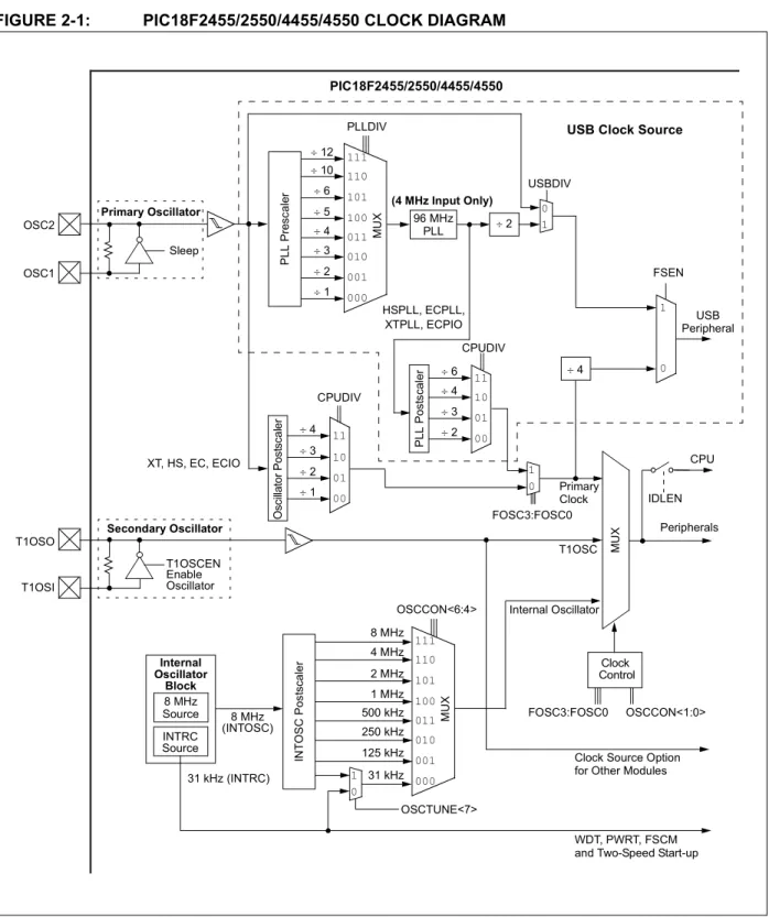
Devices in the PIC18F2455/2550/4455/4550 family incorporate a different oscillator and microcontroller clock system than previous PIC18F devices. The addi-tion of the USB module, with its unique requirements for a stable clock source, make it necessary to provide a separate clock source that is compliant with both USB low-speed and full-speed specifications.
To accommodate these requirements, PIC18F2455/ 2550/4455/4550 devices include a new clock branch to provide a 48 MHz clock for full-speed USB operation. Since it is driven from the primary clock source, an additional system of prescalers and postscalers has been added to accommodate a wide range of oscillator frequencies. An overview of the oscillator structure is shown in Figure 2-1.
Other oscillator features used in PIC18 enhanced microcontrollers, such as the internal oscillator block and clock switching, remain the same. They are discussed later in this chapter.
2.1.1 OSCILLATOR CONTROL
The operation of the oscillator in PIC18F2455/2550/ 4455/4550 devices is controlled through two Configu-ration registers and two control registers. ConfiguConfigu-ration registers, CONFIG1L and CONFIG1H, select the oscillator mode and USB prescaler/postscaler options. As Configuration bits, these are set when the device is programmed and left in that configuration until the device is reprogrammed.
The OSCCON register (Register 2-2) selects the Active Clock mode; it is primarily used in controlling clock switching in power-managed modes. Its use is discussed in Section 2.4.1 “Oscillator Control Register”.
The OSCTUNE register (Register 2-1) is used to trim the INTRC frequency source, as well as select the low-frequency clock source that drives several special features. Its use is described in Section 2.2.5.2 “OSCTUNE Register”.
2.2
Oscillator Types
PIC18F2455/2550/4455/4550 devices can be operated in twelve distinct oscillator modes. In contrast with pre-vious PIC18 enhanced microcontrollers, four of these modes involve the use of two oscillator types at once. Users can program the FOSC3:FOSC0 Configuration bits to select one of these modes:
1. XT Crystal/Resonator
2. HS High-Speed Crystal/Resonator 3. HSPLL High-Speed Crystal/Resonator
with PLL Enabled
4. EC External Clock with FOSC/4 Output 5. ECIO External Clock with I/O on RA6 6. ECPLL External Clock with PLL Enabled
and FOSC/4 Output on RA6 7. ECPIO External Clock with PLL Enabled,
I/O on RA6
8. INTHS Internal Oscillator used as Microcontroller Clock Source, HS Oscillator used as USB Clock Source 9. INTIO Internal Oscillator used as
Microcontroller Clock Source, EC Oscillator used as USB Clock Source, Digital I/O on RA6
10. INTCKO Internal Oscillator used as Microcontroller Clock Source, EC Oscillator used as USB Clock Source, FOSC/4 Output on RA6
2.2.1 OSCILLATOR MODES AND
USB OPERATION
Because of the unique requirements of the USB module, a different approach to clock operation is necessary. In previous PIC® devices, all core and peripheral clocks
were driven by a single oscillator source; the usual sources were primary, secondary or the internal oscilla-tor. With PIC18F2455/2550/4455/4550 devices, the pri-mary oscillator becomes part of the USB module and cannot be associated to any other clock source. Thus, the USB module must be clocked from the primary clock source; however, the microcontroller core and other peripherals can be separately clocked from the secondary or internal oscillators as before.
FIGURE 2-1: PIC18F2455/2550/4455/4550 CLOCK DIAGRAM PIC18F2455/2550/4455/4550 FOSC3:FOSC0 Secondary Oscillator T1OSCEN Enable Oscillator T1OSO T1OSI
Clock Source Option for Other Modules OSC1
OSC2
Sleep
Primary Oscillator
XT, HS, EC, ECIO
T1OSC CPU Peripherals IDLEN IN T O SC Po s ts c a le r MU X MU X 8 MHz 4 MHz 2 MHz 1 MHz 500 kHz 125 kHz 250 kHz OSCCON<6:4> 111 110 101 100 011 010 001 000 31 kHz INTRC Source Internal Oscillator Block
WDT, PWRT, FSCM 8 MHz Internal Oscillator (INTOSC) Clock Control OSCCON<1:0> Source 8 MHz
31 kHz (INTRC)
0 1
OSCTUNE<7>
and Two-Speed Start-up 96 MHz PLL PLLDIV CPUDIV 0 1 0 1
÷ 2
PL L Pr e s c a le r MU X 111 110 101 100 011 010 001 000
÷ 1
÷ 2
÷ 3
÷ 4
÷ 5
÷ 6
÷ 10
÷ 12
11 10 01 00 PL L Po s ts c a le r
÷ 2
÷ 3
÷ 4
÷ 6
USB USBDIV FOSC3:FOSC0 HSPLL, ECPLL, 11 10 01 00 Oscilla to r Po st sca le r
÷ 1
÷ 2
÷ 3
÷ 4
CPUDIV
1
0
Peripheral FSEN
÷ 4
USB Clock Source
XTPLL, ECPIO
Primary Clock
2.2.2 CRYSTAL OSCILLATOR/CERAMIC RESONATORS
In HS, HSPLL, XT and XTPLL Oscillator modes, a crystal or ceramic resonator is connected to the OSC1 and OSC2 pins to establish oscillation. Figure 2-2 shows the pin connections.
The oscillator design requires the use of a parallel cut crystal.
FIGURE 2-2: CRYSTAL/CERAMIC
RESONATOR OPERATION (XT, HS OR HSPLL
CONFIGURATION)
TABLE 2-1: CAPACITOR SELECTION FOR
CERAMIC RESONATORS
Note: Use of a series cut crystal may give a fre-quency out of the crystal manufacturer’s specifications.
Note 1: See Table 2-1 and Table 2-2 for initial values of C1 and C2.
2: A series resistor (RS) may be required for AT strip cut crystals.
3: RF varies with the oscillator mode chosen. C1(1)
C2(1) XTAL
OSC2 OSC1
RF(3)
Sleep To
Logic
PIC18FXXXX
RS(2)
Internal
Typical Capacitor Values Used: Mode Freq OSC1 OSC2
XT 4.0 MHz 33 pF 33 pF
HS 8.0 MHz
16.0 MHz
27 pF 22 pF
27 pF 22 pF
Capacitor values are for design guidance only.
These capacitors were tested with the resonators listed below for basic start-up and operation. These values are not optimized.
Different capacitor values may be required to produce acceptable oscillator operation. The user should test the performance of the oscillator over the expected VDD and temperature range for the application.
See the notes following Table 2-2 for additional information.
Resonators Used:
4.0 MHz 8.0 MHz 16.0 MHz
TABLE 2-2: CAPACITOR SELECTION FOR CRYSTAL OSCILLATOR
An internal postscaler allows users to select a clock frequency other than that of the crystal or resonator. Frequency division is determined by the CPUDIV Configuration bits. Users may select a clock frequency of the oscillator frequency, or 1/2, 1/3 or 1/4 of the frequency.
An external clock may also be used when the micro-controller is in HS Oscillator mode. In this case, the OSC2/CLKO pin is left open (Figure 2-3).
FIGURE 2-3: EXTERNAL CLOCK INPUT
OPERATION (HS OSC CONFIGURATION)
2.2.3 EXTERNAL CLOCK INPUT
The EC, ECIO, ECPLL and ECPIO Oscillator modes require an external clock source to be connected to the OSC1 pin. There is no oscillator start-up time required after a Power-on Reset or after an exit from Sleep mode.
In the EC and ECPLL Oscillator modes, the oscillator frequency divided by 4 is available on the OSC2 pin. This signal may be used for test purposes or to synchronize other logic. Figure 2-4 shows the pin connections for the EC Oscillator mode.
FIGURE 2-4: EXTERNAL CLOCK
INPUT OPERATION (EC AND ECPLL CONFIGURATION)
The ECIO and ECPIO Oscillator modes function like the EC and ECPLL modes, except that the OSC2 pin becomes an additional general purpose I/O pin. The I/O pin becomes bit 6 of PORTA (RA6). Figure 2-5 shows the pin connections for the ECIO Oscillator mode.
FIGURE 2-5: EXTERNAL CLOCK
INPUT OPERATION (ECIO AND ECPIO CONFIGURATION)
The internal postscaler for reducing clock frequency in XT and HS modes is also available in EC and ECIO modes.
Osc Type Crystal Freq
Typical Capacitor Values Tested:
C1 C2
XT 4 MHz 27 pF 27 pF
HS 4 MHz 27 pF 27 pF
8 MHz 22 pF 22 pF
20 MHz 15 pF 15 pF
Capacitor values are for design guidance only.
These capacitors were tested with the crystals listed below for basic start-up and operation. These values are not optimized.
Different capacitor values may be required to produce acceptable oscillator operation. The user should test the performance of the oscillator over the expected VDD and temperature range for the application.
See the notes following this table for additional information.
Crystals Used:
4 MHz 8 MHz 20 MHz
Note 1: Higher capacitance increases the stability of oscillator but also increases the start-up time.
2: When operating below 3V VDD, or when using certain ceramic resonators at any voltage, it may be necessary to use the HS mode or switch to a crystal oscillator.
3: Since each resonator/crystal has its own characteristics, the user should consult the resonator/crystal manufacturer for appropriate values of external components.
4: Rs may be required to avoid overdriving crystals with low drive level specification.
5: Always verify oscillator performance over the VDD and temperature range that is expected for the application.
OSC1
OSC2 Open
Clock from
Ext. System PIC18FXXXX
(HS Mode)
OSC1/CLKI
OSC2/CLKO FOSC/4
Clock from
Ext. System PIC18FXXXX
OSC1/CLKI
I/O (OSC2) RA6
Clock from
2.2.4 PLL FREQUENCY MULTIPLIER
PIC18F2455/2550/4255/4550 devices include a Phase Locked Loop (PLL) circuit. This is provided specifically for USB applications with lower speed oscillators and can also be used as a microcontroller clock source.
The PLL is enabled in HSPLL, XTPLL, ECPLL and ECPIO Oscillator modes. It is designed to produce a fixed 96 MHz reference clock from a fixed 4 MHz input. The output can then be divided and used for both the USB and the microcontroller core clock. Because the PLL has a fixed frequency input and output, there are eight prescaling options to match the oscillator input frequency to the PLL.
There is also a separate postscaler option for deriving the microcontroller clock from the PLL. This allows the USB peripheral and microcontroller to use the same oscillator input and still operate at different clock speeds. In contrast to the postscaler for XT, HS and EC modes, the available options are 1/2, 1/3, 1/4 and 1/6 of the PLL output.
The HSPLL, ECPLL and ECPIO modes make use of the HS mode oscillator for frequencies up to 48 MHz. The prescaler divides the oscillator input by up to 12 to produce the 4 MHz drive for the PLL. The XTPLL mode can only use an input frequency of 4 MHz which drives the PLL directly.
FIGURE 2-6: PLL BLOCK DIAGRAM
(HS MODE)
2.2.5 INTERNAL OSCILLATOR BLOCK
The PIC18F2455/2550/4455/4550 devices include an internal oscillator block which generates two different clock signals; either can be used as the microcontroller’s clock source. If the USB peripheral is not used, the internal oscillator may eliminate the need for external oscillator circuits on the OSC1 and/or OSC2 pins.
The main output (INTOSC) is an 8 MHz clock source which can be used to directly drive the device clock. It also drives the INTOSC postscaler which can provide a range of clock frequencies from 31 kHz to 4 MHz. The INTOSC output is enabled when a clock frequency from 125 kHz to 8 MHz is selected.
The other clock source is the internal RC oscillator (INTRC) which provides a nominal 31 kHz output. INTRC is enabled if it is selected as the device clock source; it is also enabled automatically when any of the following are enabled:
• Power-up Timer • Fail-Safe Clock Monitor • Watchdog Timer • Two-Speed Start-up
These features are discussed in greater detail in
Section 25.0 “Special Features of the CPU”. The clock source frequency (INTOSC direct, INTRC direct or INTOSC postscaler) is selected by configuring the IRCF bits of the OSCCON register (page 33).
2.2.5.1 Internal Oscillator Modes
When the internal oscillator is used as the micro-controller clock source, one of the other oscillator modes (External Clock or External Crystal/Resonator) must be used as the USB clock source. The choice of the USB clock source is determined by the particular internal oscillator mode.
There are four distinct modes available:
1. INTHS mode: The USB clock is provided by the oscillator in HS mode.
2. INTXT mode: The USB clock is provided by the oscillator in XT mode.
3. INTCKO mode: The USB clock is provided by an external clock input on OSC1/CLKI; the OSC2/ CLKO pin outputs FOSC/4.
4. INTIO mode: The USB clock is provided by an external clock input on OSC1/CLKI; the OSC2/ CLKO pin functions as a digital I/O (RA6).
Of these four modes, only INTIO mode frees up an additional pin (OSC2/CLKO/RA6) for port I/O use.
MU
X
VCO Loop Filter and
Prescaler OSC2
OSC1
PLL Enable
FIN FOUT
SYSCLK Phase
Comparator HS/EC/ECIO/XT Oscillator Enable
÷24 (from CONFIG1H Register)
2.2.5.2 OSCTUNE Register
The internal oscillator’s output has been calibrated at the factory but can be adjusted in the user’s applica-tion. This is done by writing to the OSCTUNE register (Register 2-1). The tuning sensitivity is constant throughout the tuning range.
The INTOSC clock will stabilize within 1 ms. Code exe-cution continues during this shift. There is no indication that the shift has occurred.
The OSCTUNE register also contains the INTSRC bit. The INTSRC bit allows users to select which internal oscillator provides the clock source when the 31 kHz frequency option is selected. This is covered in greater detail in Section 2.4.1 “Oscillator Control Register”.
2.2.5.3 Internal Oscillator Output Frequency and Drift
The internal oscillator block is calibrated at the factory to produce an INTOSC output frequency of 8.0 MHz. However, this frequency may drift as VDD or tempera-ture changes, which can affect the controller operation in a variety of ways.
The low-frequency INTRC oscillator operates indepen-dently of the INTOSC source. Any changes in INTOSC across voltage and temperature are not necessarily reflected by changes in INTRC and vice versa.
REGISTER 2-1: OSCTUNE: OSCILLATOR TUNING REGISTER
R/W-0 U-0 U-0 R/W-0 R/W-0 R/W-0 R/W-0 R/W-0
INTSRC — — TUN4 TUN3 TUN2 TUN1 TUN0
bit 7 bit 0
Legend:
R = Readable bit W = Writable bit U = Unimplemented bit, read as ‘0’
-n = Value at POR ‘1’ = Bit is set ‘0’ = Bit is cleared x = Bit is unknown
bit 7 INTSRC: Internal Oscillator Low-Frequency Source Select bit
1 = 31.25 kHz device clock derived from 8 MHz INTOSC source (divide-by-256 enabled) 0 = 31 kHz device clock derived directly from INTRC internal oscillator
bit 6-5 Unimplemented: Read as ‘0’ bit 4-0 TUN4:TUN0: Frequency Tuning bits
01111 = Maximum frequency
• • • • 00001
00000 = Center frequency. Oscillator module is running at the calibrated frequency.
11111
• • • •
2.2.5.4 Compensating for INTOSC Drift
It is possible to adjust the INTOSC frequency by modifying the value in the OSCTUNE register. This has no effect on the INTRC clock source frequency.
Tuning the INTOSC source requires knowing when to make the adjustment, in which direction it should be made and in some cases, how large a change is needed. When using the EUSART, for example, an adjustment may be required when it begins to generate framing errors or receives data with errors while in Asynchronous mode. Framing errors indicate that the device clock frequency is too high; to adjust for this, decrement the value in OSCTUNE to reduce the clock frequency. On the other hand, errors in data may sug-gest that the clock speed is too low; to compensate, increment OSCTUNE to increase the clock frequency.
It is also possible to verify device clock speed against a reference clock. Two timers may be used: one timer is clocked by the peripheral clock, while the other is clocked by a fixed reference source, such as the Timer1 oscillator. Both timers are cleared but the timer clocked by the reference generates interrupts. When an interrupt occurs, the internally clocked timer is read and both timers are cleared. If the internally clocked timer value is greater than expected, then the internal oscillator block is running too fast. To adjust for this, decrement the OSCTUNE register.
Finally, a CCP module can use free-running Timer1 (or Timer3), clocked by the internal oscillator block and an external event with a known period (i.e., AC power frequency). The time of the first event is captured in the CCPRxH:CCPRxL registers and is recorded for use later. When the second event causes a capture, the time of the first event is subtracted from the time of the second event. Since the period of the external event is known, the time difference between events can be calculated.
2.3
Oscillator Settings for USB
When these devices are used for USB connectivity, they must have either a 6 MHz or 48 MHz clock for USB operation, depending on whether Low-Speed or Full-Speed mode is being used. This may require some forethought in selecting an oscillator frequency and programming the device.
The full range of possible oscillator configurations compatible with USB operation is shown in Table 2-3.
2.3.1 LOW-SPEED OPERATION
The USB clock for Low-Speed mode is derived from the primary oscillator chain and not directly from the PLL. It is divided by 4 to produce the actual 6 MHz clock. Because of this, the microcontroller can only use a clock frequency of 24 MHz when the USB module is
active and the controller clock source is one of the primary oscillator modes (XT, HS or EC, with or without the PLL).
This restriction does not apply if the microcontroller clock source is the secondary oscillator or internal oscillator block.
2.3.2 RUNNING DIFFERENT USB AND
MICROCONTROLLER CLOCKS
The USB module, in either mode, can run asynchro-nously with respect to the microcontroller core and other peripherals. This means that applications can use the primary oscillator for the USB clock while the micro-controller runs from a separate clock source at a lower speed. If it is necessary to run the entire application from only one clock source, full-speed operation provides a greater selection of microcontroller clock frequencies.
TABLE 2-3: OSCILLATOR CONFIGURATION OPTIONS FOR USB OPERATION
Input Oscillator Frequency
PLL Division (PLLDIV2:PLLDIV0)
Clock Mode (FOSC3:FOSC0)
MCU Clock Division (CPUDIV1:CPUDIV0)
Microcontroller Clock Frequency
48 MHz N/A(1) EC, ECIO None (00) 48 MHz
÷2 (01) 24 MHz
÷3 (10) 16 MHz
÷4 (11) 12 MHz
48 MHz ÷12 (111) EC, ECIO None (00) 48 MHz
÷2 (01) 24 MHz
÷3 (10) 16 MHz
÷4 (11) 12 MHz
ECPLL, ECPIO ÷2 (00) 48 MHz
÷3 (01) 32 MHz
÷4 (10) 24 MHz
÷6 (11) 16 MHz
40 MHz ÷10 (110) EC, ECIO None (00) 40 MHz
÷2 (01) 20 MHz
÷3 (10) 13.33 MHz
÷4 (11) 10 MHz
ECPLL, ECPIO ÷2 (00) 48 MHz
÷3 (01) 32 MHz
÷4 (10) 24 MHz
÷6 (11) 16 MHz
24 MHz ÷6 (101) HS, EC, ECIO None (00) 24 MHz
÷2 (01) 12 MHz
÷3 (10) 8 MHz
÷4 (11) 6 MHz
HSPLL, ECPLL, ECPIO ÷2 (00) 48 MHz
÷3 (01) 32 MHz
÷4 (10) 24 MHz
÷6 (11) 16 MHz
20 MHz ÷5 (100) HS, EC, ECIO None (00) 20 MHz
÷2 (01) 10 MHz
÷3 (10) 6.67 MHz
÷4 (11) 5 MHz
HSPLL, ECPLL, ECPIO ÷2 (00) 48 MHz
÷3 (01) 32 MHz
÷4 (10) 24 MHz
÷6 (11) 16 MHz
16 MHz ÷4 (011) HS, EC, ECIO None (00) 16 MHz
÷2 (01) 8 MHz
÷3 (10) 5.33 MHz
÷4 (11) 4 MHz
HSPLL, ECPLL, ECPIO ÷2 (00) 48 MHz
÷3 (01) 32 MHz
÷4 (10) 24 MHz
÷6 (11) 16 MHz
12 MHz ÷3 (010) HS, EC, ECIO None (00) 12 MHz
÷2 (01) 6 MHz
÷3 (10) 4 MHz
÷4 (11) 3 MHz
HSPLL, ECPLL, ECPIO ÷2 (00) 48 MHz
÷3 (01) 32 MHz
÷4 (10) 24 MHz
÷6 (11) 16 MHz
8 MHz ÷2 (001) HS, EC, ECIO None (00) 8 MHz
÷2 (01) 4 MHz
÷3 (10) 2.67 MHz
÷4 (11) 2 MHz
HSPLL, ECPLL, ECPIO ÷2 (00) 48 MHz
÷3 (01) 32 MHz
÷4 (10) 24 MHz
÷6 (11) 16 MHz
4 MHz ÷1 (000) XT, HS, EC, ECIO None (00) 4 MHz
÷2 (01) 2 MHz
÷3 (10) 1.33 MHz
÷4 (11) 1 MHz
HSPLL, ECPLL, XTPLL, ECPIO
÷2 (00) 48 MHz
÷3 (01) 32 MHz
÷4 (10) 24 MHz
÷6 (11) 16 MHz
TABLE 2-3: OSCILLATOR CONFIGURATION OPTIONS FOR USB OPERATION (CONTINUED)
Input Oscillator Frequency
PLL Division (PLLDIV2:PLLDIV0)
Clock Mode (FOSC3:FOSC0)
MCU Clock Division (CPUDIV1:CPUDIV0)
Microcontroller Clock Frequency
2.4
Clock Sources and Oscillator
Switching
Like previous PIC18 enhanced devices, the PIC18F2455/2550/4455/4550 family includes a feature that allows the device clock source to be switched from the main oscillator to an alternate, low-frequency clock source. These devices offer two alternate clock sources. When an alternate clock source is enabled, the various power-managed operating modes are available.
Essentially, there are three clock sources for these devices:
• Primary oscillators • Secondary oscillators • Internal oscillator block
The primary oscillators include the External Crystal and Resonator modes, the External Clock modes and the internal oscillator block. The particular mode is defined by the FOSC3:FOSC0 Configuration bits. The details of these modes are covered earlier in this chapter.
The secondary oscillators are those external sources not connected to the OSC1 or OSC2 pins. These sources may continue to operate even after the controller is placed in a power-managed mode.
PIC18F2455/2550/4455/4550 devices offer the Timer1 oscillator as a secondary oscillator. This oscillator, in all power-managed modes, is often the time base for functions such as a Real-Time Clock (RTC). Most often, a 32.768 kHz watch crystal is connected between the RC0/T1OSO/T13CKI and RC1/T1OSI/ UOE pins. Like the XT and HS Oscillator mode circuits, loading capacitors are also connected from each pin to ground. The Timer1 oscillator is discussed in greater detail in Section 12.3 “Timer1 Oscillator”.
In addition to being a primary clock source, the internal oscillator block is available as a power-managed mode clock source. The INTRC source is also used as the clock source for several special features, such as the WDT and Fail-Safe Clock Monitor.
2.4.1 OSCILLATOR CONTROL REGISTER
The OSCCON register (Register 2-2) controls several aspects of the device clock’s operation, both in full-power operation and in power-managed modes.
The System Clock Select bits, SCS1:SCS0, select the clock source. The available clock sources are the primary clock (defined by the FOSC3:FOSC0 Configu-ration bits), the secondary clock (Timer1 oscillator) and the internal oscillator block. The clock source changes immediately after one or more of the bits is written to, following a brief clock transition interval. The SCS bits are cleared on all forms of Reset.
The Internal Oscillator Frequency Select bits, IRCF2:IRCF0, select the frequency output of the internal oscillator block to drive the device clock. The choices are the INTRC source, the INTOSC source (8 MHz) or one of the frequencies derived from the INTOSC postscaler (31 kHz to 4 MHz). If the internal oscillator block is supplying the device clock, changing the states of these bits will have an immediate change on the internal oscil-lator’s output. On device Resets, the default output frequency of the internal oscillator block is set at 1 MHz.
When an output frequency of 31 kHz is selected (IRCF2:IRCF0 = 000), users may choose which inter-nal oscillator acts as the source. This is done with the INTSRC bit in the OSCTUNE register (OSCTUNE<7>). Setting this bit selects INTOSC as a 31.25 kHz clock source by enabling the divide-by-256 output of the INTOSC postscaler. Clearing INTSRC selects INTRC (nominally 31 kHz) as the clock source.
This option allows users to select the tunable and more precise INTOSC as a clock source, while maintaining power savings with a very low clock speed. Regardless of the setting of INTSRC, INTRC always remains the clock source for features such as the Watchdog Timer and the Fail-Safe Clock Monitor.
The OSTS, IOFS and T1RUN bits indicate which clock source is currently providing the device clock. The OSTS bit indicates that the Oscillator Start-up Timer (OST) has timed out and the primary clock is providing the device clock in primary clock modes. The IOFS bit indicates when the internal oscillator block has stabilized and is providing the device clock in RC Clock modes. The T1RUN bit (T1CON<6>) indicates when the Timer1 oscil-lator is providing the device clock in secondary clock modes. In power-managed modes, only one of these three bits will be set at any time. If none of these bits are set, the INTRC is providing the clock or the internal oscillator block has just started and is not yet stable.
The IDLEN bit determines if the device goes into Sleep mode, or one of the Idle modes, when the SLEEP instruction is executed.
The use of the flag and control bits in the OSCCON register is discussed in more detail in Section 3.0 “Power-Managed Modes”.
Note 1: The Timer1 oscillator must be enabled to select the secondary clock source. The Timer1 oscillator is enabled by setting the T1OSCEN bit in the Timer1 Control regis-ter (T1CON<3>). If the Timer1 oscillator is not enabled, then any attempt to select a secondary clock source will be ignored.