Carolina Fidalgo Marques
Bachelor of Science in Engineering of Micro and Nanotechnologies
Perovskite Photovoltaic Materials:
towards a flexible and low cost solar
cell technology
Dissertation to obtain the Master Degree in Engineering of Micro and Nanotechnologies
Supervisor: Elvira Maria Correia Fortunato
Full Professor, Universidade Nova de Lisboa
Co-supervisor: Manuel João de Moura Dias Mendes
Marie Curie Post-Doc Fellow, Universidade Nova de
Lisboa
Jury President:Examiner: To be announced
Member:
III
Perovskite Solar Cells – Towards a flexible and low cost solar cell
Copyright©
Carolina Fidalgo Marques, Faculdade de Ciências e Tecnologia, Universidade Nova de Lisboa
A Faculdade de Ciências e Tecnologia e a Universidade Nova de Lisboa têm o direito, perpétuo e sem limites geográficos, de arquivar e publicar esta dissertação através de exemplares
V
“For a successful technology, reality must take precedence over public relations, for Nature cannot be fooled.”
“Study hard what interests you the most in the most undisciplined, irreverent and original manner possible.”
“You have no responsibility to live up to what other people think you ought to accomplish. I have no responsibility to be like they expect me to be. It's their mistake, not my failing.”
VII
Acknowledgements
Em primeiro lugar, gostaria de agradecer à minha orientadora, Prof.ª Dra. Elvira Fortunato, pela oportunidade de trabalhar num tema ainda tão recente e com tanto para oferecer. Não poderia deixar de agradecer também ao Presidente do Departamento de Materiais, Prof. Dr. Rodrigo Martins por se ter preocupado sempre em garantir boas condições de trabalho para os seus alunos. Agradeço também ao meu co-orientador, Manuel Mendes, por ter confiado em mim e no meu método de trabalho. O que me remete para o Alexandre Fonseca, por ser a única pessoa com quem podia falar de perovskite sem olhar para mim como se fosse maluca.
Não podia deixar de agradecer a toda a equipa do CENIMAT e CEMOP pelos sorrisos, pela companhia e pela competência: Sónia Pereira, Alexandra Gonçalves, Raquel Água, Rita Branquinho, Emanuel Carlos (Manu!), Daniela Gomes, Ana Rovisco, Sofia Ferreira, Olalla Sanchez, Tiago Mateus e Paul Grey. Em especial à minha homónima, Carolina Marques, só porque quis escrever o meu nome numa linha especial dos agradecimentos. E aos professores Luís Pereira e Pedro Barquinha, por me ensinarem praticamente tudo o que sei até hoje.
Ao pessoal do Tico e Quês, que se expandiu para 202 e Quês, por todos os cafés, todas as noitadas a escrever relatórios, todas as maratonas de estudo à última da hora e por todos os anos de carinho e amizade: Ana Figueiredo, Ana Gaspar, António Almeida, Bruno Fernandes, Carolina Natal, Constança Oliveira, Daniel Fernandes, Gabriel Pires de Souza, Gonçalo Santos, Jaime Machado Faria, Joana Almeida, João Ribas, Pedro Pinto, Ricardo Farinha e Sofia Chamiço. Sem vós, eu não teria conseguido. E aos amigos que, por razões de força maior (PREGUIÇA), estão mais presentes de modo virtual: Ricardo Ramos, Joana Salgueiro, José Rosa, Nuno Pereira e Raquel Ariosa.
Ao melhor professor de Ballet do mundo, João Cabaça, por me ensinar que os limites estão na minha cabeça. E claro, às meninas todas por me ajudarem a manter a sanidade mental.
Aos meus amigos patudos por todo o amor incondicional: Goya, Miró, Shéu. Em especial ao Jonas pelas diretas a escrever a tese. Mas o meu agradecimento mais especial vai para o Simão, o cão movido a pão. Onde quer que estejas, espero que estejas rodeado!
Ao Tomás, por todos os abraços que me impediram de atirar o computador pela varanda e por seres o melhor companheiro que poderia pedir nesta aventura que é a vida.
IX
Abstract
The exploitation of solar energy has become a necessity for sustainable development. One of the approaches has been the use of photovoltaic materials to convert this never-ending energy source in electrical energy. For this approach to be reliable, it ought to combine high efficiency with low production costs, while also promising flexible devices. Perovskite structured compounds act as the light harvesting material in solar cells and can be produced using simple methods such as solvent-engineering and spin coating. This work focuses on the study of perovskite compounds ABX3, where A is methylammonium or caesium cations, B is a lead cation and X is a halide ion such as bromine, chlorine and iodine. These films were produced via spin coating and the solvent-mix used was DMF:DMSO in different ratios (2:3, 3:2 and 4:1). The influence of toluene dropping during the spinning process was also studied. The careful tuning of these processes allowed the formation of poly-crystalline perovskite films, deposited on top of Glass/FTO/ZTO-NPs, that presented optical absorbance values between 80-90% and optical bandgaps of 1.5 eV for MAPbI3 and 1.7 eV for MAPbI2Br0.85Cl0.15, as expected from the state-of-art materials.
Keywords: renewable energy, flexible and low-cost thin-film photovoltaics,
XI
Resumo
A exploração da energia solar tornou-se numa necessidade para um desenvolvimento sustentável. Uma das abordagens tem sido a utilização de materiais fotovoltaicos para a conversão desta fonte de energia renovável em energia elétrica. Para que esta abordagem seja segura, deve combinar alta eficiência com baixos custos de produção e a promessa de dispositivos flexíveis. Compostos com a estrutura da perovskite atuam como material activo numa célula solar e podem ser produzidos usando métodos simples como solvent-engineering e spin-coating. Este trabalho
apresenta um estudo de compostos de perovskite ABX3, onde o A é um catião de metilamónio ou césio, o B é um catião de chumbo e o X é um haleto (bromo, cloro e/ou iodo). Estes filmes foram produzidos via spin-coating e a mistura de solventes usada foi DMF:DMSO com diferentes rácios
(2:3, 3:2, 4:1). Foi também estudada a influência da adição de tolueno durante o processo de
spinning. O ajuste destes processos permitiu a formação de filmes de perovskite policristalinos,
depositados em cima de vidro/FTO/ZTO-NPs, com valores de absorvância entre 80-90%, e hiatos ópticos de 1.5 eV para MAPbI3 e 1.7 eV para MAPbI2Br0.85Cl0.15, o que está de acordo com o
state-of-art.
XIII
Index of contents
1 Introduction ... 1
1.1 Perovskite Solar Cell ... 1
1.1.1 Perovskite Structure ... 1
1.1.2 Perovskite Solar Cell Architecture ... 4
1.1.3 Electron Transport Layer... 4
1.1.4 Hole Transport Layer ... 5
2 Materials and Methods ... 7
2.1 Zinc Tin Oxide (Zn2SnO4) Nanoparticles Synthesis ... 7
2.1.1 Hydrothermal Synthesis ... 7
2.1.2 Solution-processed Synthesis ... 7
2.2 Precursor Solutions Preparation ... 7
2.2.1 ETL Precursor Solution ... 7
2.2.2 HTL Precursor solution ... 7
2.2.3 Perovskite precursor solutions... 7
2.2.4 Thin Films Deposition ... 8
2.3 Characterization ... 8
2.3.1 SEM-EDS ... 8
2.3.2 XRD ... 9
2.3.3 UV-Vis Spectroscopy ... 9
3 Results and Discussion ... 11
3.1 Zn2SnO4 Nanoparticles Characterization ... 11
3.2 Perovskite Thin Film Characterization... 12
3.2.1 Morphological Characterization ... 13
3.2.2 Structural Characterization ... 15
3.2.3 Optical Characterization ... 19
3.3 Solar Cells ... 21
4 Conclusions and Future Perspectives ... 25
4.1.1 Future perspectives ... 26
5 References ... 27
XIV
Appendix B ... 36
Appendix C ... 40
Appendix D ... 42
XV
Index of figures
XVI
Figure 18 - Schematic of the solar cell envisioned. ... 22 Figure 19 - SEM-FIB Cross section of MAPbI3 solar cells: a,c) 150 uL; b,d) 750 uL. ... 22 Figure 20 – EDS mapping of the cross section of a MAPbI3 solar cell produced with 150 µL of toluene. The scale bars are 1µm. ... 23 Figure 21 - Spectrums of the EDS mapping of the cross section of the MAPbI3 solar cell. ... 23 Figure 22 – EDS mapping of the cross section of a MAPbI3 solar cell produced with 750 µL. The scale bars are 1µm. ... 24 Figure 23 - Spectrums of the EDS mapping of the cross section of a MAPbI3 solar cell produced with 750 µL. The scale bar is 1µm. ... 24
Figure A 1 - Formation mechanism of ZSO NPs. (a) Schematic illustration of the formation mechanism of crystalline ZSO NPs via low-temperature process. (b) Formation map of ZSO with different temperature and hydrazine/Zn ratio. Image from [31] ... 31 Figure A 2 – SEM image of nanoparticles resultant from solution-processed synthesis of Zn2SnO4 at 90ºC. These nanoparticles have around 20 nm of diameter. ... 32 Figure A 3 - SEM image of the nanoparticles resultant from the solution-processed synthesis of Zn2SnO4 at 100ºC with the aid of a heating mantle. Nanoparticle sizes are around 20-30 nm. .. 32 Figure A 4 - SEM image of nanoparticles resultant from the hydrothermal synthesis of Zn2SnO4. Nanoparticle size vary from 20 to 100 nm. ... 33 Figure A 5 - SEM-EDS mapping images of the product resultant from the solution-processed synthesis at 90ºC with no heating mantle. The scale bars are 2.5 µm. ... 33 Figure A 6 -EDS spectrums of the product obtained with low-temperature synthesis of Zn2SnO4. Scale bar is 2.5 µm. ... 34 Figure A 7 – SEM-EDS mapping images and spectrum of low-temperature solution-processed synthesis of Zn2SnO4 at 100ºC with a heating mantle. The scale bars are 1 µm... 34 Figure A 8 – EDS spectrum of ZTO NPs produced by hydrothermal method. The scale bar is 2.5 µm. ... 35
XVII Figure B 5 - SEM-EDS mapping images of MAPbI3 with a solvent-mix ratio DMF:DMSO of 2:3. Scale bar is 2.5 µm. ... 37 Figure B 6 - SEM-EDS spectrum of MAPbI3 with a solvent-mix ratio DMF:DMSO of 2:3 ... 38 Figure B 7 - SEM-EDS mapping of MA0.9Cs0.1PbI3 with a solvent-mix ratio DMF:DMSO of 4:1. The volume of toluene added during the spin coating process was 750 µL. The scale bars are 2.5 µm. ... 38 Figure B 8 - SEM-EDS mapping of MA0.9Cs0.1PbI3 with a solvent-mix ratio DMF:DMSO of 3:2. The volume of toluene added during the spin coating process was 750 µL. The scale bars are 2.5 µm. ... 38 Figure B 9 - SEM-EDS mapping of MA0.9Cs0.1PbI2Br0.85Cl0.15 with a solvent-mix ratio DMF:DMSO of 4:1. The volume of toluene added during the spin coating process was 750 µL. The scale bars are 2.5 µm. ... 39 Figure B 10 - SEM-EDS mapping of MA0.9Cs0.1PbI2Br0.85Cl0.15 with a solvent-mix ratio DMF:DMSO of 2:3. The volume of toluene added during the spin coating process was 750 µL. The scale bars are 2.5 µm. ... 39
Figure D 1 - Optical absorbance of a perovskite samples with linear fitting to determine the optical bandgap. ... 42
XIX
Index of tables
Table 1- Silicon solar cells vs. Perovskite solar cells. ... XXV Table 2 - Influence of the electron transport layer on PSC factors. ... 4 Table 3 - Quantities of each reagent for 1M of perovskite. ... 8 Table 4 - the Goldschmidt tolerance factor calculated for six pristine perovskites: MAPbI3, MAPbBr3, MAPbCl3, CsPbI3, CsPbBr3, CsPbCl3. ... 16 Table 5 - Optical bandgaps calculated from the optical absorption for MAPbI3 and MA0.9Cs0.1PbI3 samples. ... 19 Table 6 - Optical bandgaps calculated from the optical absorption for MAPbI2Br0.85Cl0.15 and MACsPbI2Br0.85Cl0.15 samples. ... 21
XXI
Abbreviations
DMF – N,N-dimethylformamide
DMSO – Dimethyl Sulfoxide
FTO – Fluorine-doped tin oxide
ETL – Electron Transport Layer
EDS – Energy Dispersive Spectroscopy
HTL – Hole transport Layer
MA0.9Cs0.1PbI3– Caesium-doped Methylammonium Lead Iodide
MA0.9Cs0.1PbI2Br0.85Cl0.15–Caesium-doped Methylammonium Lead Trihalide
MAPbI3– Methylammonium Lead Iodide
MAPbI2Br0.85Cl0.15–Methylammonium Lead Trihalide
PSC – Perovskite Solar Cell
Rpm – rotations per minute
SEM – Scanning Electron Microscopy
Spiro-MeOTAD - 2,2’,7,7’-tetrakis(N,N-di-p-meth-oxyphenylamine)-9’,9’-spirobifluorene
TCO – Transparent Conducting Oxide
UV – Ultraviolet
Uv-Vis – Ultraviolet-Visible
XRD – X-ray Diffraction
ZTO – Zinc Tin Oxide Nanoparticles produced by hydrothermal method
ZTO NPs – Zinc Tin Oxide Nanoparticles
XXIII
Symbols
Br – Bromine
Cl – Chlorine
Cs – Caesium
CsI – Caesium Iodide
cm - centimeter
CuSCN – Copper Thiocyanate
EPH– Photon energy
Eg– Optical bandgap
h – hour
I – Iodine
IPA – 2-propanol
M – Molar concentration
MA – Methylammonium
MAI – Methylammonium Iodide
MABr – Methylammonium Bromide
min – Minute
mL – milliliter
mm - milimeter
N2H4.H2O – Hydrazine hydrate
NaCO3 – Sodium carbonate
Pb – Lead
PbCl2– Lead chloride
PbBr2– Lead bromide
PbI2– Lead iodide
s – Second
SnCl2.5H2O – Tin Chloride Pentahydrate
SnO2– Tin dioxide
TiO2 – Titanium dioxide
ZnCl2– Zin dichloride
ZnO – Zinc oxide
Zn2SnO4– Zinc Tin Oxide
°C – Degrees Celsius
Ω– ohm
XXV
Motivation and Objectives
Silicon has been the favored photovoltaic material in microelectronics. However, there is demand for a semiconductor able to combine low-temperature solution-processability with efficient fulfilment of the three primary functions of a solar cell active layer: light absorption, free-carrier generation, and transport of both holes and electrons to their selective contacts with minimum losses. A new generation of mixed-organic halide perovskites offers prospects on higher energy conversion efficiencies and lower processing costs.
The lowest cost and highest throughput method of fabrication is solution based production. It is hard to envisage a solar technology breaking into the large-scale power market unless it can compete closely with c-Si on efficiency, and beat it on price. The usual requirement of high temperatures for processing limits the choice of possible substrates.
Table 1- Silicon solar cells vs. Perovskite solar cells.
Silicon Solar cells Perovskite Solar Cells
Expensive, multistep process conducted at high temperatures in high vacuum and special clean room facilities
Simpler wet chemistry techniques in a traditional laboratory environment.
Solvent and vapor deposition techniques.
An ideal solar cell requires low cost, trouble free, abundant material resources with good stability and high-power conversion and should be able to be integrated into a large area device.
The main goal of this work was to pave the way towards producing a flexible and low cost solar cell, using a novel perovskite-structured material as the active layer. For that, and with the temperature dependence of flexible substrates, all the materials chosen had to be low-cost and easily fabricated.
This work was divided in:
Optimization of the production of zin tin oxide (Zn2SnO4) nanoparticles through a large-scale solution method;
study of perovskite materials thin films and its dependence on the anti-solvent (toluene), solvent mix ratio and doping;
1
1
Introduction
A solar cell is an electronic device that takes advantage of the photovoltaic effect in which electromagnetic radiation is converted into electrical energy. For that, a material in which the absorption of light causes the excitation of an electron, and its consequent dislocation to the external circuit of the solar cell, is needed.
When a solar cell is illuminated, if the photon energy is higher than the band gap of the semiconductor material (EPH > Eg), electron-hole pairs are generated (EHP) which are then collected, generating an external current. This is the main principle of a solar cell. In summary, there are three essential steps towards a working solar cell: electron-hole generation, minority carriers separation, and its sub sequential collection.
Figure 1 - Solar device scheme.
1.1
Perovskite Solar Cell
A perovskite solar cell (PSC) includes a perovskite structured compound, most commonly a hybrid organic-inorganic lead halide-based material, as the light-harvesting active layer. These materials are cheap to produce and simple to manufacture.
1.1.1
Perovskite Structure
2
energy, while having high absorption coefficient and charge carrier mobility, functioning as an ambipolar layer and absorbing broadly across the solar spectrum. [5]–[8]
These perovskite absorbers do not require expensive and complicated techniques, resulting from simple preparation, such as solution-processing, spin coating or printing. In addition, perovskite can be solution-processed in air under low temperature conditions, positioning it as a promising material for photovoltaic devices.[8]–[10] The possibility to tune the optical properties of the organo-metal halide perovskite paves the way to high voltage cells.[4], [9]
Figure 2 – Structure models of MAPbI3 with a) cubic, b) tetragonal and c) orthorhombic structures. Image adapted from [11]
The crystal structure of perovskite materials can be cubic, tetragonal or orthorhombic (Figure 2)
which can also be estimated using the Goldschmidt tolerance factor.[4] This factor is explained in Appendix C. The electronic properties of organometallic halides depend on various factors
which can be controlled experimentally. These factors include lattice constants, which can be varied by applying external pressure or internal chemical pressure; the type of halide ion, controlled by chemical substitution; and the type of organic ion. [12]
1.1.1.1
Halide Influence
3
1.1.1.2
A-Cation Influence
The organic compound tunes the binding exciton energy as it influences the dielectric constant.[9] The cation (A) in ABX3 perovskites commonly includes alkylammonium (e.g. methylammonium, caesium, etc.). The identity of the A cation strongly influences the band gap and electronic properties of perovskites through its influence on the crystal structure. [19] Recent studies have revealed that the introduction of Cs+ cations in small quantities (10 mol%) can effectively alter the crystalline lattice, modulate the thermodynamic phase stability, and control the film formation of hybrid perovskites.[20] Partial replacement of MAI with CsI in the precursor solution influences the crystallization rate and film formation of perovskites, not affecting significantly the resulting optical gap. [21] The similar size of Cs+ and MA+ cations allows Cs ions to substitute and coexist with MA without fundamentally changing the crystal structure. [19]
1.1.1.3
Spin Coating
Spin coating is one of the cheapest film production methods, being widely used in solution-processed perovskite solar cells. Evaporation and the convective self-assembly process during spinning induces the immediate formation of well-crystallized perovskite materials due to strong ionic interactions between the metal cations and halogen ions.[22]
Pre-heating both the substrate and precursor solutions results in more uniform and highly crystalline thin films, and the use of toluene washing has been reported to lead to fast crystallization and short thermal annealing times. The rapid change in film color from yellow to reddish-brown, shown in Figure 3, shows crystalline perovskite formation after adding the
anti-solvent during spinning. When toluene reacts with the perovskite solution, forces its precursors to precipitate. Hence, the volume of anti-solvent used is very critical for reproducible efficient perovskite cells.[23]
Figure 3 - Scheme of the solvent washing process. Adapted from [23]
1.1.1.4
Solvent Influence
4
while the relatively higher evaporation rate of DMF facilitates solvent evaporation during spin coating.[24]
1.1.2
Perovskite Solar Cell Architecture
The cell structures used can be classified into two types: porous and planar architectures (Figure
4). Early perovskite solar cells were based on a mesoporous oxide structure that is commonly
used in dye-sensitized solar cells.[25] The titanium dioxide (TiO2) mesoporous layer in perovskite solar cells has an important role in electron transport, as well as in the mechanical support of the perovskite crystal as a scaffold.[26] However, mesoporous layer-based devices require high-temperature sintering, which precludes the use of either plastic substrates or roll-to-roll processing. To overcome the issue, the planar perovskite solar cell was developed and showed comparable performance.[9], [27], [28]
Figure 4 - Representative scheme of a mesoporous PSC (right) and planar PSC (left).
The ability to use perovskite in sensitized or planar architecture, in addition to its ambipolar properties, are competitive advantages towards achieving high power conversion efficiencies.
1.1.3
Electron Transport Layer
The main goal for an electron transport layer (ETL) is to extract photo generated electrons from perovskite and transport these charges to electrodes. Its influence on several factors can be observed in Table 2. [29]
Table 2 - Influence of the electron transport layer on PSC factors.
Factor Influence
Energy level Charge injection and recombination
Trap states Charge recombination and transport
Electron mobility Charge transport and collection
Interface Charge recombination
5 The most used material for ETL is TiO2, a semiconductor oxide with favorable energy level, easy fabrication, and long electron lifetimes. However, it also shows low electron mobility, high density of electronic trap states below the conduction band, and it requires high-temperature processing, which presents a serious problem for flexible solar cells production. [25] For that, a zinc oxide (ZnO) layer was introduced as an alternative ETL, which presented better electron mobility than titanium oxide and low temperature preparation.[28] However, its chemical and thermal instability made this material a poor solution.[29] A tin dioxide (SnO2) layer has also been employed with the advantages of possessing excellent optical properties and good stability, however a hysteresis behavior is associated with this material.[30] To solve these problems, zinc tin oxide (ZTO) nanoparticles films have been introduced as a more favorable electron extractors in perovskite solar cells. This material is prepared in solution below 100 ºC and some of its appealing properties are: a conduction band edge position similar to TiO2 and ZnO, and its chemical stability with respect to acid/base solution and polar organic solvents which make it an excellent candidate for solution processing. [31]
1.1.4
Hole Transport Layer
7
2
Materials and Methods
2.1
Zinc Tin Oxide (Zn
2SnO
4) Nanoparticles Synthesis
Two different methods were used to produce Zn2SnO4 nanoparticles: a small scale hydrothermal synthesis, and a large-scale solution-processed synthesis. Both methods used zinc dichloride (ZnCl2, Sigma-Aldrich) as the zinc source and tin chloride pentahydrate (SnCl2.5H2O, Sigma-Aldrich) as the tin source.
2.1.1
Hydrothermal Synthesis
ZnCl2 and SnCl4.5H20 were dissolved separately in deionized water to form two transparent solutions. Then, the tin tetrachloride solution was slowly added to the zinc chloride solution (Zn:Sn ratio of 2:1). Sodium carbonate (NaCO3), used as a mineralizer, was dissolved in deionized water and added dropwise to the mixture under magnetic stirring. After stirring for 15 min, the solution (15 mL) was transferred into an autoclave (Model 4744, Parr) and subjected to hydrothermal conditions at 200 °C for 24h and then cooled at room temperature. The resulting precipitates were washed with deionized water and ethanol via centrifugation. These nanoparticles will be referred as ZTO.
2.1.2
Solution-processed Synthesis
ZnCl2 and SnCl4.5H20 (2:1) were dissolved in deionized water (80 mL) under vigorous magnetic stirring. Hydrazine hydrate (N2H4.H20) was added with a molar ratio N2H4:Zn of 8:1 and the resultant solution was heated on a hot plate, with and without a heating mantle, at 100 °C for 18h. The obtained products were washed with deionized water and ethanol via centrifugation. These nanoparticles will be referred as ZSO.
2.2
Precursor Solutions Preparation
2.2.1
ETL Precursor Solution
The electron transport layer precursor solution was prepared dissolving the ZTO powder in IPA (15 mg ml-1) via ultrasonication for 30 minutes, resulting in a milky solution.
2.2.2
HTL Precursor solution
The hole transport layer precursor was prepared by dissolving copper(I) thiocyanate (Sigma-Aldrich) in dipropyl sulphide (Sigma-(Sigma-Aldrich) with a concentration of 15 mg ml-1. The solution was stirred for 48h.
2.2.3
Perovskite precursor solutions
8
(MA0.9Cs0.1PbI2Br0.85Cl0.15). All the reagents were purchased from Sigma-Aldrich. The powders used were methylammonium iodide (MAI), methylammonium bromide (MABr), caesium iodide(CsI), lead iodide (PbCl2), lead bromide (PbBr2) and lead chloride (PbCl2). The solvent mix was produced with dimethylformamide (DMF) and dimethyl sulfoxide (DMSO) with ratios (DMF:DMSO) of 4:1, 3:2, 2:3 and 1:3. These solutions were made with a concentration of 1M and then stirred at 60 °C until it turned into a translucid yellow solution. Table 3 presents the
quantities used for 1 ml of precursor solution for each perovskite
Table 3 - Quantities of each reagent for 1M of perovskite.
Reagents
(mmol) MAPbI3 MA0.9Cs0.1PbI3 MAPbI2Br0.85Cl0.15 MA0.9Cs0.1PbI2Br0.85Cl0.15
MAI 1 0.9 0.5 0.4
MABr - 0.1 0.5 0.5
CsI - 0.1
PbI2 1 0.75
PbBr2 - 0.15
PbCl2 - 0.1
2.2.4
Thin Films Deposition
Fluorine-doped tin oxide (FTO) coated glass (100 mm x 100 mm x 2.2 mm, 13 Ω/sq, 82-84.5% transmittance) were obtained from Sigma-Aldrich and cut into smaller pieces of 2.5 × 2.5 cm2 to be used as the spin coating substrates. These substrates were then cleaned with detergent and deionized water and then placed in an ultrasonic bath in IPA for 15 min, followed by a 15 min UV treatment. Afterwards, a ZTO thin film was spin coated for 30 s at 4000 rpm.
The substrates and the perovskite precursor solutions were heated at 70 °C. Perovskite thin films were deposited by spin coating a single layer of the perovskite precursor solutions (1M) using a 2-step method that consisted in 10 s step at 1000 rpm followed by a 20 s step at 5000 rpm followed by an immediate hot plate annealing at 100 °C for 15 min. Toluene was added in the final 10 s with volumes between 0 and 750 µL.
2.3
Characterization
2.3.1
SEM-EDS
9
2.3.2
XRD
The structural analysis of both ZTO/ZSO nanoparticles and perovskite thin films was done by X-ray diffraction (XRD) using a PANalyticalX’Pert Pro X-ray diffractometer in Bragg–Brentano geometry, with a monochromatic Cu-Kα radiation source (wavelength 1.5406 Å). XRD measurements were carried out from 10 ° to 65 º (2θ). The spectra analysis was acquired with High Score Plus software (PANalytical).
2.3.3
UV-Vis Spectroscopy
11
3
Results and Discussion
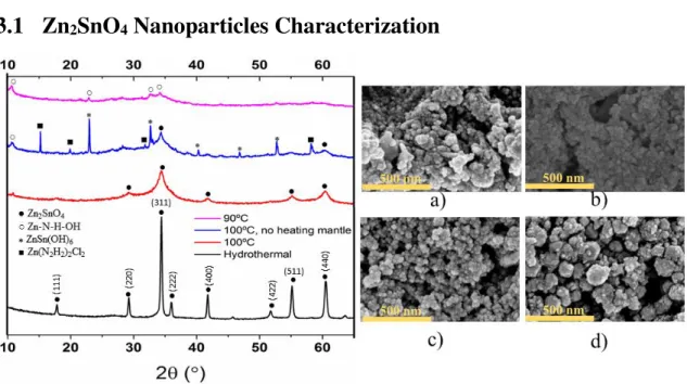
3.1
Zn
2SnO
4Nanoparticles Characterization
Figure 5 - XRD diffractogram of the results using different synthesis methods (left) and SEM images (right) of the samples: Solution-processed synthesis: a) at 90ºC; b) at 100ºC with no heating mantle; c) at 100ºC with a heating mantle. d) Hydrothermal Synthesis. EDS mapping can be found on Appendix A.
In the hydrothermal method, ZnSn(OH)6 forms from the slurries of Sn and Zn by consuming OH -ions. The mineralizer used, NaCO3, can continuously supply OH- ions until all the intermediate hydroxide is fully converted to Zn2SnO4 (Reactions 1-4 – Appendix A). No impurities are formed because the nanoparticles can be effectively formed from both Zn(OH)4 and Sn(OH)6 ions (Reaction 5–Appendix A), which can be confirmed with the XRD patterns showed in Figure
5. The size of the nanoparticles obtained was in a range from 20-150 nm (Figure A4–Appendix A).
12
(Figure A3–Appendix A) and it can be explained with the lack of homogeneity throughout the
volume of the synthesis solution.
At last, the reaction performed at 100 ºC with the aid of a heating mantle presents a diffractogram similar to the one obtained for ZTO, confirming that Zn2SnO4 was indeed present. The greater height of ZTO peaks indicate a larger particle size related to ZSO, which is confirmed with SEM images. The range of sizes for the ZSO nanoparticles obtained were in the range of 20-30 nm (Figure A2 – Appendix A).
3.2
Perovskite Thin Film Characterization
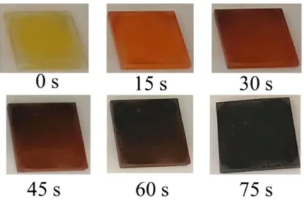
Figure 6 - Change of color during the annealing process of a MAPbI3 perovskite thin film.
Perovskite thin films deposited by spin-coating are not easily reproduced, since the way the anti-solvent is dropped can affect the uniformity of the obtained film, such as the round defect in the middle of the MAPbI3 samples showed in Figure 6. By the end of the spin-coating process, the MAPbI3 samples presented a darker color than the MAPbI2Br0.85Cl0.15 samples, which can be explained by the crystallization rate being slower when bromide is present. As the crystallization process occurs, it can be observed a change in the color from reddish-brown to brown, and then grey-black in MAPbI3 perovskites (Figure 6), and from yellow, to orange, to brown, and finally to grey-black in MAPbI2Br0.85Cl0.15 perovskites (Figure 7).
13
3.2.1
Morphological Characterization
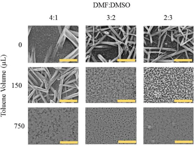
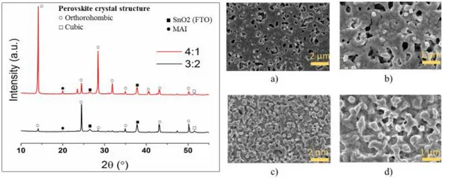
Control over the morphology and coverage of high-quality perovskite films is the main issue affecting planar-structured perovskite solar cells fabricated by solution processing. The morphology of perovskite films was investigated for different solvent-mix ratios, and volumes of toluene dropped during the spin-coating process. The SEM images in Figure 8 show the changes
in morphology of the prepared perovskite films. The EDS mapping of the perovskite samples can be found in Appendix B.
3.2.1.1
Methylammonium triiodide perovskite
Figure 8 - SEM images of MAPbI3 samples with different solvent mix ratios used and different toluene volumes added. The scale bar is 10 µm.
As observed in Figures 8 and 9, when no toluene is dropped during the spin-coating processing
it affects the way perovskite crystallizes resulting in poor coverage of the substrate (Figure B1-
Appendix B), which can be confirmed for the three solvent-mix ratios used. When dropping 150
14
precursors, leaving a narrower window of opportunity for humidity to react with the hygroscopic methylammonium cation, since films are extremely moisture-sensitive until fully crystallized. Hence, the drier the sample is before the annealing process, the more uniform the film morphology will be.
DMSO has a low evaporation rate and high viscosity and it functions both as a solvent and as a coordination reagent, in the form of PbI2-MAI-DMSO complex; while DMF only functions as a solvent with a relatively higher evaporation rate than DMSO. The formation of the PbI2 -MAI-DMSO intermediate-phase film retards the rapid reaction between PbI2 and MAI during the evaporation of DMF. It is observable in both Figures 8 and 9 that, when DMF is the main solvent
(4:1 ratio), results in several large bundles of perovskite with lengths over 10 µm woven together in a network on the surface of the substrate, even when 150 µL of toluene is dropped during solvent washing. Even though these bundles are still formed when more DMSO is used, the surface coverage starts to improve. As toluene is added, the difference between ratios is accentuated.
15
3.2.1.2
Methylammonium lead trihalide perovskite
Figure 10 - SEM images of MA0.9Cs0.1PbI2Br0.85Cl0.15 samples with different solvent mix ratios and toluene volume added. Sample with * was not doped with Caesium. The scale bar is 10 µm.
As observed in MAPbI3 samples (Figures 6 and 7), when no toluene is added during the spin coating process, poor coverage is obtained (Figure 10). This coverage improves with the toluene
volume added, with films becoming smoother and appearing more continuous with the increase of toluene. As mentioned in section 3.2.1.1, DMF is used as the main solvent while DMSO is
used as a coordination reagent. It is still observed the formation of bundles when no toluene was added during the film deposition, however, differences between triiodide and trihalide perovskites appear even when only 150 µL of toluene is added. In this case, not even with excess DMF the formation of bundles is observed. In trihalide perovskite, the influence of caesium appears to be beneficent as the films become more continuous when this element is present. The presence of bromide and chloride presents a visible change in the manner that perovskite crystallizes.
3.2.2
Structural Characterization
Methylammonium lead halides can have three different crystalline phases – cubic, tetragonal and orthorhombic (Figure 2) – and these phases transition with temperature (Table B3 –Appendix
16
2.06 Å for I-, 1.82 Å for Br- and 1.67 Å for Cl-. The tolerance factor was calculated for the six pristine perovskites that could be formed with the reagents that were used, and the results are presented in Table 4.
Table 4 - the Goldschmidt tolerance factor calculated for six pristine perovskites: MAPbI3, MAPbBr3, MAPbCl3, CsPbI3, CsPbBr3, CsPbCl3.
Perovskite MAPbI3 MAPbBr3 MAPbCl3 CsPbI3 CsPbBr3 CsPbCl3 Tolerance
factor 0.81 0.82 0.82 0.85 0.86 0.87
The tolerance factor values calculated indicates that, at room temperature, methylammonium lead halides are not in the ideal cubic structure, but instead adopting a preferential orthorhombic structure. The structural characterization that follows was based on a MAPbI3 crystal structure study performed by Takeo Oku, where each crystalline phase was characterized in their characteristic temperature range, to assure that each peak would correspond to only the phase that was being studied.[11]
3.2.2.1
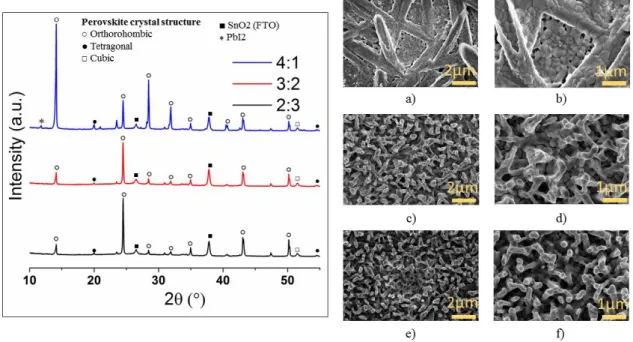
Methylammonium triiodide perovskite
Figure 11 - XRD diffractogram of MAPbI3 perovskites with different DMF:DMSO ratios (left) and SEM images of the same samples: a,b) MAPbI3 4:1; c,d) MAPbI3 3:2; e,f) MAPbI3 2:3. The scale bars are 2µm (left) and 1 µm (right).
As expected, these triiodide perovskites adopted an orthorhombic crystal phase, predicted by the Goldschmidt tolerance factor calculated in Table 4. However, it is also noticeable that, when the
17 perovskites prefer to grow, which may explain the differences in the films morphology, observable in Figure 11 (a-f). When Cs+ was added, a change in peak intensity occurred. For the
solvent-mix of 4:1, the crystal shows preferential growth in two distinct planes which may explain the inexistence of bundles (Figure 12 a and b) when compared to the un-doped one (Figure 11 a and b).
Figure 12 - XRD diffractogram of MA0.9Cs0.1PbI3 with different DMF:DMSO ratios (left) and SEM images of the same samples: a,b) MA0.9Cs0.1PbI3 4:1; c,d) MA0.9Cs0.1PbI3 3:2. . The scale bars are 2µm (left) and 1 µm (right).
In all cases, the peaks of the FTO appear, which is due to lack of surface coverage and the existence of pinholes. This can be confirmed with the EDS characterization in Appendix B.
3.2.2.2
Methylammonium Lead Trihalide Perovskite
18
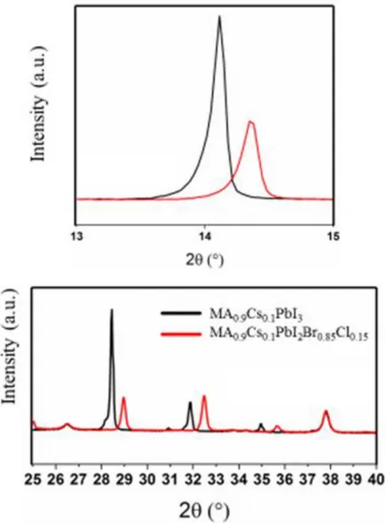
In trihalide perovskites, there is also a prominent peak referent to PbI2 when no toluene is added to the spin coating process. In this case, regardless the solvent-mix ratio, all the samples have the same preferred peak as the most intense one. The main difference is the fact that, contrary to what was observed for MACsPbI3, the worst surface coverage was obtained with the solvent-mix ratio of 2:3 (Figure B10–Appendix B). The structural difference between the two perovskites seems
to originate from the differences in the ionic radii of the halides (Table B2 – Appendix B). The
smaller X ion radius is relatively beneficial for the formation of cubic structure, which can be confirmed by the appearance of a cubic crystal structure peak in the diffractogram.
Figure 14 - XRD intensity peaks of MA0.9Cs0.1PbI3 and MA0.9Cs0.1PbI2Br0.85Cl0.15.
When comparing MA0.9Cs0.1PbI3 and MA0.9Cs0.1PbI2B0.85Cl0.15 diffractograms, it was observed that when bromide and chloride were added the peaks shifted to the right (Figure 14), which can
19
3.2.3
Optical Characterization
3.2.3.1
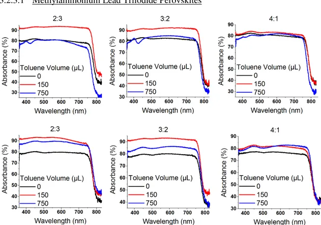
Methylammonium Lead Triiodide Perovskites
Figure 15 – Optical absorption as a function of the wavelength for MAPbI3 (top images) and MACsPbI3 (bottom images) with different solvent-mix ratios.
The optical absorption of triiodide perovskites (Figure 15) demonstrated to be stronger when less
DMF was used in the precursor solution. This is related to the improved surface coverage resultant from the change of solvent-mix ratio from 4:1 to 3:2 and 2:3 (Figures 8 and 9). However, even
though the samples where 750 µL of toluene were added seem to present an improved surface coverage, their absorbance is lower than the ones where 150 µL were added, which is probably due to changes in film thickness. With these data, and since an integrating sphere was used, the optical bandgap of each sample was calculated using the method explained in Appendix D and
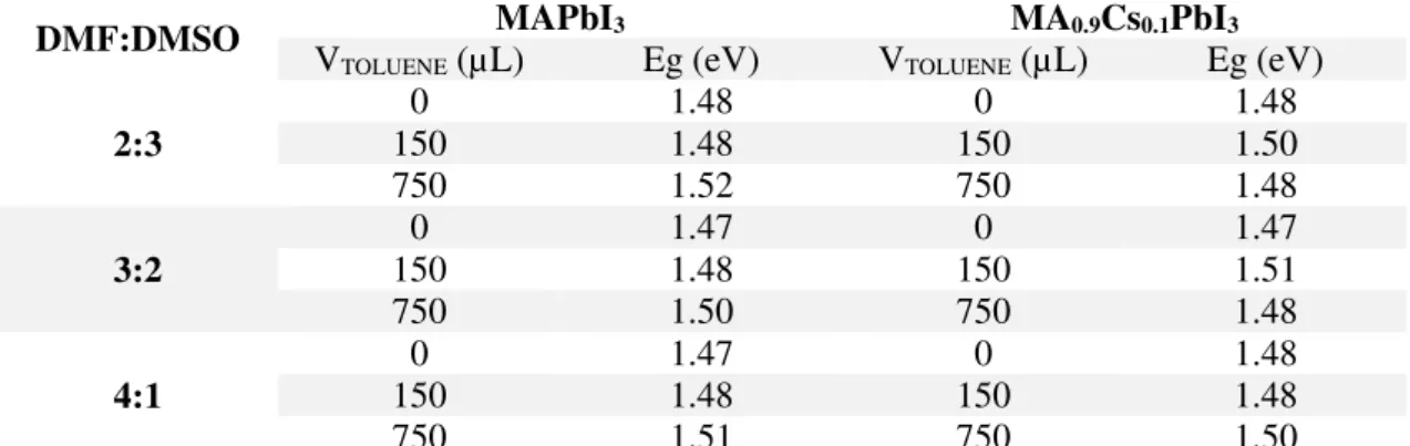
the results are shown in Table 5. The Eg was around 1.5 eV in all samples.
20
DMF:DMSO V MAPbI3 MA0.9Cs0.1PbI3
TOLUENE (µL) Eg (eV) VTOLUENE (µL) Eg (eV)
2:3
0 1.48 0 1.48
150 1.48 150 1.50
750 1.52 750 1.48
3:2
0 1.47 0 1.47
150 1.48 150 1.51
750 1.50 750 1.48
4:1
0 1.47 0 1.48
150 1.48 150 1.48
750 1.51 750 1.50
3.2.3.2
Methylammonium Lead Trihalide Perovskites
Figure 16 - Optical absorption as a function of the wavelength for different solvent-mix ratios. MAPbI2Br0.85Cl0.15 (top left image) and MACsPbI2Br0.85Cl0.15 (top right and bottom images)
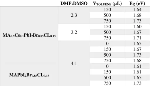
21 bromide and chloride reduces the lattice constant. The optical bandgaps values calculated were around 1.6-1.7 eV and are presented in Table 6.
Table 6 - Optical bandgaps calculated from the optical absorption for MAPbI2Br0.85Cl0.15 and MACsPbI2Br0.85Cl0.15 samples.
DMF:DMSO VTOLUENE (µL) Eg (eV)
MA0.9Cs0.1PbI2Br0.85CL0.15
2:3
150 1.64 500 1.68 750 1.73
3:2
150 1.60 500 1.67 750 1.71
4:1
0 1.65
150 1.67 500 1.73 750 1.68
MAPbI2Br0.85CL0.15
0 1.61
150 1.61 500 1.65 750 1.73
In section 3.2.3.2, the perovskite materials present an optimal bandgap for single junction solar cells, similar to those of record devices. [36], [37] In section 3.2.3.2, it can be observed a consistent increase of 1-2 eV in the bandgap, which has been investigated in the literature to develop wide-bandgap perovskite films, mainly envisaged for the top cell of double-junction devices with Si-based bottom cell. [38]
3.3
Solar Cells
Figure 17 - MAPbI3 solar cells with different DMF:DMSO ratios: 2:3 (left), 3:2 (center), 4:1 (rigth).
To investigate the behaviour of the perovskite thin films produced as a photovoltaic material, solar cells were produced (Figure 17). The ETL and HTL chosen were ZTO and CuSCN,
respectively, as shown in Figure 18. However, it was not possible to obtain an IV curve when
22
Figure 18 - Schematic of the solar cell envisioned.
Even though the perovskite thin films produced present an optimal band gap for a solar cell, absorbing throughout the visible spectrum, and the morphology of the films presented numerous alternatives paths for which the current may travel, thereby short-circuiting the devices. To better understand the reason behind the non-functioning cell, images of cross section of the films were acquired by SEM (Figure 19).
Figure 19 - SEM-FIB Cross section of MAPbI3 solar cells: a,c) 150 uL; b,d) 750 uL.
23 cell, as it can be seen in the EDS analysis (Figures 20 and 21). In this EDS mapping, it can be
perceived that the aluminium penetrated the perovskite film, creating a more favourable path for the current created through the photovoltaic material.
Figure 20 – EDS mapping of the cross section of a MAPbI3 solar cell produced with 150 µL of toluene. The scale bars are 1µm.
24
Figure 22 – EDS mapping of the cross section of a MAPbI3 solar cell produced with 750 µL. The scale bars are 1µm.
Figure 23 - Spectrums of the EDS mapping of the cross section of a MAPbI3 solar cell produced with 750 µL. The scale bar is 1µm.
25
4
Conclusions and Future Perspectives
This work presented a study of solution-processed perovskite thin film materials, envisaged for low cost and flexible solar cells. For that, the photovoltaic devices ought to be fully constituted with inexpensive materials that can be processed at low temperatures. The study also focused in the production of Zn2SnO4 nanoparticles to work as an ETL, as they can be deposited at room temperature.
Two methods were used to produce zin tin oxide (Zn2SnO4) nanoparticles. The hydrothermal method is simple, cost-effective with high reproducibility and good control over the composition and morphology, as long as the temperature is high enough to convert the hydroxides in Zn2SnO4. [39] However, it requires an autoclave and high temperature, making this technique not approachable for a simple production. In view of, a different approach was studied: a large-scale solution-processed synthesis. Even though the literature states that this method can produce nanoparticles at T=90ºC[31], the nanoparticles produced at that temperature were ZnSn(OH)6, which meant the temperature was not enough to convert it in zinc tin oxide. The temperature was raised to 100ºC but still the result was not the expected. Then, a heating mantle was applied to uniformize the temperature throughout the solution resulting in zinc tin oxide nanoparticles with a uniform range of sizes between 20-30 nm (Figure 5c); as opposite of those obtained via
hydrothermal method, which had a larger range of sizes from 20-150 nm (Figure 5d).
The second part of this work was consisted in the study of four types of perovskite compounds: methylammonium lead triiodide (MAPbI3), caesium-doped methylammonium lead triiodide (MA0.9Cs0.1PbI3), methylammonium lead trihalide (MAPbI2Br0.85Cl0.15) and caesium-doped methylammonium lead trihalide (MA0.9Cs0.1PbI2Br0.85Cl0.15). For the precursor solutions, a solvent-mix of DMF:DMSO was used with variable ratios: 4:1, 3:2, 2:3. These perovskite thin films were produced via spin-coating in air which difficulted the perovskite crystallization without defects (Figures 8-10).
XRD diffractograms (Figure 11 and 12) showed that, when crystallized at 100 ⁰C in air, the
26
either by a disordered orientation or by a mobility of the cation in the crystal. The disordering of the MA+ occupation is reduced only when this crystal structure transitions to an orthorhombic symmetry, getting a fixed position.[40]
As for the solar cells, poor morphology can lead to electrical shorting and affect charge/transport/separation and recombination. One step solution-processed perovskite solar cells with planar geometries have issues to solve such as an inhomogeneous surface morphology (Figure 8-10), irregular crystallinity (Figure 11-13) and poor reproducibility. Also, perovskite
crystallinity has a great effect on charge separation, transport and diffusion length, as for the defects in crystals behave as trap sites resulting in charge recombination. [23] Therefore, the poor response obtained with the solar cells produced is mainly attributed to pin-hole formation and incomplete coverage of the perovskite resulting in low-resistance shunting paths and low light absorption in the solar cell. [41]
4.1.1
Future perspectives
The perovskite films produced were porous, therefore this solar cell may benefit from an insulating TiO2 paste that can prevent short circuiting while extracting the photo generated carriers.
To produce perovskite films with improved morphology, a precursor compound (HPbI3) could be the answer to the formation of highly uniform, dense and thick films of MAPbI3.[42] Also, the addition of formamidium (FA+) as a A-cation has been shown to improve thin film uniformity and continuity, and reduces the amount of pinholes and defects.[1]
The main goal of this study was to focus on a perovskite solar cell that could be flexible and low-cost, hence the HTL and ETL materials chosen. So, an obvious step would be, after optimizing all the layers of the solar cell structure, extend this research to flexible substrates such as FTO/ITO-coated PET/PEN.
Another approach could be the incorporation of this wide band-gap materials in a tandem cell. MACsPbI2Br0.85Cl0.15 produced presented band gaps near 1.7 eV, which would be ideal for a top cell together with silicon, which has a bandgap of 1.1 eV. [4] [38]
27
5
References
[1] G. E. Eperon, S. D. Stranks, C. Menelaou, M. B. Johnston, L. M. Herz, and H. J. Snaith,
“Formamidinium lead trihalide: a broadly tunable perovskite for efficient planar heterojunction
solar cells,” Energy Environ. Sci., vol. 7, no. 3, p. 982, 2014.
[2] J. H. Noh, S. H. Im, J. H. Heo, T. N. Mandal, and S. Il Seok, “Chemical management for colorful,
efficient, and stable inorganic-organic hybrid nanostructured solar cells,” Nano Lett., vol. 13, no.
4, pp. 1764–1769, 2013.
[3] B. Cai, Y. D. Xing, Z. Yang, W. H. Zhang, and J. S. Qiu, “High performance hybrid solar cells sensitized by organolead halide perovskites,” Energy Environ. Sci., vol. 6, no. 5, pp. 1480–1485,
2013.
[4] J. T. Jacobsson, J. P. Correa Baena, M. Pazoki, M. Saliba, K. Schenk, M. Grätzel, and A. Hagfeldt,
“An exploration of the compositional space for mixed lead halogen perovskites for high efficiency
devices - SI,” Energy Environ. Sci., vol. 41, no. 0, pp. 1–35, 2016.
[5] B. Conings, L. Baeten, T. Jacobs, R. Dera, J. D’Haen, J. Manca, and H. G. Boyen, “An easy -to-fabricate low-temperature TiO2 electron collection layer for high efficiency planar heterojunction perovskite solar cells,” APL Mater., vol. 2, no. 8, 2014.
[6] J. M. Ball, M. M. Lee, A. Hey, and H. J. Snaith, “Low-temperature processed meso-superstructured to thin-film perovskite solar cells,” Energy Environ. Sci., vol. 6, no. 6, p. 1739, 2013.
[7] V. D’Innocenzo, G. Grancini, M. J. P. Alcocer, A. R. S. Kandada, S. D. Stranks, M. M. Lee, G.
Lanzani, H. J. Snaith, and A. Petrozza, “Excitons versus free charges in organo-lead tri-halide
perovskites.,” Nat. Commun., vol. 5, p. 3586, 2014.
[8] S. D. Stranks, G. E. Eperon, G. Grancini, C. Menelaou, M. J. P. Alcocer, T. Leijtens, L. M. Herz,
A. Petrozza, and H. J. Snaith, “Electron-Hole Diffusion Lengths Exceeding 1 Micrometer in an
Organometal Trihalide Perovskite Absorber,” Science (80-. )., vol. 342, no. 6156, pp. 341–344,
2013.
[9] S. Gamliel and L. Etgar, “Organo-metal perovskite based solar cells: sensitized versus planar
architecture,” RSC Adv., vol. 4, p. 29012, 2014.
[10] C. Wehrenfennig, M. Liu, H. J. Snaith, M. B. Johnston, and L. M. Herz, “Charge carrier recombination channels in the low-temperature phase of organic-inorganic lead halide perovskite
thin films,” APL Mater., vol. 2, no. 8, 2014.
28
[12] R. A. Jishi, “Modified Becke-Johnson exchange potential: improved modeling of lead halides for
solar cell applications,” Aims Mater. Sci., vol. 3, no. 1, pp. 149–159, 2016.
[13] B. Suarez, V. Gonzalez-pedro, T. S. Ripolles, R. S. Sanchez, L. Otero, and I. Mora-sero,
“Recombination Study of Combined Halides (Cl, Br, I) Perovskite Solar Cells,” 2014.
[14] T. J. Jacobsson, L. J. Schwan, M. Ottosson, A. Hagfeldt, and T. Edvinsson, “Determination of Thermal Expansion Coefficients and Locating the Temperature-Induced Phase Transition in Methylammonium Lead Perovskites Using X-ray Diffraction,” Inorg. Chem., vol. 54, no. 22, pp.
10678–10685, 2015.
[15] M. a. Green, a. Ho-Baillie, and H. J. Snaith, “The emergence of perovskite solar cells,” Nat.
Photonics, vol. 8, no. 7, pp. 506–514, 2014.
[16] C. Quarti, E. Mosconi, P. Umari, and F. De Angelis, “Chlorine Incorporation in the CH 3 NH 3 PbI 3 Perovskite: Small Concentration, Big Effect,” Inorg. Chem., p. acs.inorgchem.6b01681, 2016.
[17] Q. Chen, H. Zhou, Y. Fang, A. Z. Stieg, T.-B. Song, H.-H. Wang, X. Xu, Y. Liu, S. Lu, J. You, P.
Sun, J. McKay, M. S. Goorsky, and Y. Yang, “The optoelectronic role of chlorine in
CH3NH3PbI3(Cl)-based perovskite solar cells,” Nat. Commun., vol. 6, pp. 1–9, 2015.
[18] B. Yuan, J. Wang, Y. Chen, X. Wu, H. Luo, S. Deng, and S. Hall, “Electronic Supplementary
Material ( ESI ) for Journal of Materials Chemistry A . This journal is © The Royal Society of Chemistry 2016 Electronic Supplementary Information Unprecedented performance of N-doped
activated hydrothermal carbon towards C 2 H 6 ,” pp. 1–16, 2016.
[19] H. Choi, J. Jeong, H. B. Kim, S. Kim, B. Walker, G. H. Kim, and J. Y. Kim, “Cesium-doped methylammonium lead iodide perovskite light absorber for hybrid solar cells,” Nano Energy, vol.
7, pp. 80–85, 2014.
[20] M. Deepa, M. Salado, L. Calio, S. Kazim, S. M. Shivaprasad, and S. Ahmad, “Cesium Power: Low Cs+ Levels Impart Stability to Perovskite Solar Cells,” Phys. Chem. Chem. Phys., 2017.
[21] X. Liu, Z. Yang, C.-C. Chueh, A. Rajagopal, S. T. Williams, Y. Sun, and A. K.-Y. Jen, “Improved
Efficiency and Stability of Pb-Sn Binary Perovskite Solar Cells by Cs Substitution,” J. Mater.
Chem. A, vol. 0, pp. 1–7, 2016.
[22] N. J. Jeon, J. H. Noh, Y. C. Kim, W. S. Yang, S. Ryu, and S. Il Seok, “Solvent engineering for
high-performance inorganic–organic hybrid perovskite solar cells,” Nat Mater, vol. 13, no. 9, pp.
897–903, 2014.
29
[24] B. Cai, W. H. Zhang, and J. Qiu, “Solvent engineering of spin-coating solutions for planar-structured high-efficiency perovskite solar cells,” Cuihua Xuebao/Chinese J. Catal., vol. 36, no. 8,
pp. 1183–1190, 2015.
[25] A. Kojima, K. Teshima, Y. Shirai, and T. Miyasaka, “Organometal halide perovskites as visible -light sensitizers for photovoltaic cells,” J. Am. Chem. Soc., vol. 131, no. 17, pp. 6050–6051, 2009.
[26] J. Burschka, N. Pellet, S.-J. Moon, R. Humphry-Baker, P. Gao, M. K. Nazeeruddin, and M. Grätzel,
“Sequential deposition as a route to high-performance perovskite-sensitized solar cells.,” Nature,
vol. 499, no. 7458, pp. 316–320, 2013.
[27] K. Hwang, Y. S. Jung, Y. J. Heo, F. H. Scholes, S. E. Watkins, J. Subbiah, D. J. Jones, D. Y. Kim,
and D. Vak, “Toward large scale roll-to-roll production of fully printed perovskite solar cells,” Adv. Mater., vol. 27, no. 7, pp. 1241–1247, 2015.
[28] D. Liu and T. L. Kelly, “Perovskite solar cells with a planar heterojunction structure prepared using
room-temperature solution processing techniques,” Nat Phot., vol. 8, no. 2, pp. 133–138, 2014.
[29] G. Yang, H. Tao, P. Qin, W. Ke, and G. Fang, “Recent progress in electron transport layers for e ffi cient perovskite solar cells,” J. Mater. Chem. A Mater. energy Sustain., vol. 4, pp. 3970–3990,
2016.
[30] J. Song, E. Zheng, X. F. Wang, W. Tian, and T. Miyasaka, “Low-temperature-processed
ZnO-SnO2 nanocomposite for efficient planar perovskite solar cells,” Sol. Energy Mater. Sol. Cells, vol. 144, pp. 623–630, 2016.
[31] S. S. Shin, W. S. Yang, J. H. Noh, J. H. Suk, N. J. Jeon, J. H. Park, J. S. Kim, W. M. Seong, and S.
Il Seok, “High-performance flexible perovskite solar cells exploiting Zn2SnO4 prepared in solution below 100 °C - supplementary infomation,” Nat. Commun., vol. 6, no. May, p. 7410, 2015.
[32] Z. Yu and L. Sun, “Recent Progress on Hole-Transporting Materials for Emerging Organometal
Halide Perovskite Solar Cells,” Adv. Energy Mater., vol. 5, no. 12, 2015.
[33] T. Swetha and S. P. Singh, “Perovskite solar cells based on small molecules hole transporting materials,” J. Mater. Chem. A, vol. 0, pp. 1–16, 2015.
[34] P. Qin, S. Tanaka, S. Ito, N. Tetreault, K. Manabe, H. Nishino, M. K. Nazeeruddin, and M. Grätzel,
“Inorganic hole conductor-based lead halide perovskite solar cells with 12.4% conversion
efficiency.,” Nat. Commun., vol. 5, no. May, p. 3834, 2014.
[35] N. K. McKinnon, D. C. Reeves, and M. H. Akabas, “5-HT3 receptor ion size selectivity is a
property of the transmembrane channel, not the cytoplasmic vestibule portals,” J. Gen. Physiol.,
30
[36] T. Salim, S. Sun, Y. Abe, A. Krishna, A. C. Grimsdale, and Y. M. Lam, “Perovskite-based solar
cells: impact of morphology and device architecture on device performance,” J. Mater. Chem. A Mater. energy Sustain., vol. 3, pp. 8943–8969, 2015.
[37] D. Bi, B. Xu, P. Gao, L. Sun, M. Grätzel, and A. Hagfeldt, “Facile synthesized organic hole transporting material for perovskite solar cell with efficiency of 19.8%,” Nano Energy, vol. 23, pp.
138–144, 2016.
[38] D. P. McMeekin, G. Sadoughi, W. Rehman, G. E. Eperon, M. Saliba, M. T. Horantner, A.
Haghighirad, N. Sakai, L. Korte, B. Rech, M. B. Johnston, L. M. Herz, and H. J. Snaith, “A mixed -cation lead mixed-halide perovskite absorber for tandem solar cells,” Science (80-. )., vol. 351, no. 6269, pp. 151–155, 2016.
[39] A. Annamalai, D. Carvalho, K. C. Wilson, and M. J. Lee, “Properties of hydrothermally synthesized Zn2SnO4 nanoparticles using Na2CO3 as a novel mineralizer,” Mater. Charact., vol. 61, no. 9, pp.
873–881, 2010.
[40] A. Poglitsch and D. Weber, “Dynamic disorder in methylammoniumtrihalogenoplumbates (II)
observed by millimeter-wave spectroscopy,” J. Chem. Phys., vol. 87, no. 11, p. 6373, 1987.
[41] G. E. Eperon, V. M. Burlakov, P. Docampo, A. Goriely, and H. J. Snaith, “Morphological control for high performance, solution-processed planar heterojunction perovskite solar cells,” Adv. Funct.
Mater., vol. 24, no. 1, pp. 151–157, 2013.
[42] F. Wang, H. Yu, H. Xu, and N. Zhao, “HPbI3: A new precursor compound for highly efficient
solution-processed perovskite solar cells,” Adv. Funct. Mater., vol. 25, no. 7, pp. 1120–1126, 2015.
[43] M. Johnsson and P. Lemmens, “Crystallography and Chemistry of Perovskites,” John Wiley Sons,
Ltd., New York, p. 11, 2007.
[44] V. M. Goldschmidt, “Die Gesetze der Krystallochemie,” Naturwissenschaften, vol. 14, no. 21, pp.
477–485, 1926.
[45] G. C. Patwardhan, S. Cao, D. H. Hatch, S. Farha, O. Hupp, J. Kanatzidis, M. G. Shatz, “Introducing
31
Appendix A
NaCO3 as a mineralizer produces an impurity-free Zn2SnO4 single phase due to its ability of continuously supplying OH- ions by hydrolysis during the reaction and thereby stabilize the solution pH value.
𝐶𝑂 32−+ 𝐻2𝑂 → 𝐻𝐶𝑂3−+ 𝑂𝐻− (1)
𝐻𝐶𝑂3−+ 𝐻2𝑂 → 𝐻2𝐶𝑂3+ 𝑂𝐻− (2)
The ions involved in this reaction can effectively form Zn2SnO4 nanoparticles without impurities as it can be seen in the reaction below.
𝑆𝑛4++ 6 𝑂𝐻−→ 𝑆𝑛(𝑂𝐻)
6 2− (3)
𝑍𝑛2++ 4 𝑂𝐻−→ 𝑍𝑛(𝑂𝐻)
4 2− (4)
𝑆𝑛(𝑂𝐻)62−+ 2 𝑍𝑛(𝑂𝐻)42−→ 𝑍𝑛2𝑆𝑛𝑂4+ 4𝐻2𝑂 + 6 𝑂𝐻− (5)
The low-temperature solution process chemical reactions can be observed in Figure A1. The
relevant parameters are the temperature and the ratio between hidrazine and zinc. A low ration results in tin oxide while a high ratio results in both ZSO and ZnSn(OH)6.
32
Figure A 2 – SEM image of nanoparticles resultant from solution-processed synthesis of Zn2SnO4 at 90ºC. These nanoparticles have around 20 nm of diameter.
33
Figure A 4 - SEM image of nanoparticles resultant from the hydrothermal synthesis of Zn2SnO4. Nanoparticle size vary from 20 to 100 nm.
34
Figure A 6 -EDS spectrums of the product obtained with low-temperature synthesis of Zn2SnO4. Scale bar is 2.5 µm.
35
Figure A 8 – EDS spectrum of ZTO NPs produced by hydrothermal method. The scale bar is 2.5 µm.
EDS mapping of the obtained products can help understanding the amount of each element present in the samples. In FigureA5 and Figure A6, it can be perceived that there is more zinc
36
Appendix B
Figure B 1- SEM-EDS mapping images of MAPbI3 with a solvent-mix ratio DMF:DMSO of 4:1. The scale bars are 2.5 µm.
In the samples where MAPbI3 with a solvent-mix ratio of 4:1 was deposited, poor coverage of the substrate was obtained, which can be observed in Figures B1 and B2, where tin can be seen in
the EDS mapping. The spectrums obtained show a great amount of tin in the bundle-uncovered section of the sample, revealing that the substrate (FTO) was not fully covered by the perovskite deposition.
37
Figure B 3 - SEM-EDS mapping images of MAPbI3 with a solvent-mix ratio DMF:DMSO of 3:2. The scale bars are 2.5 µm.
Even though no bundles are formed when using different solvent-mix ratios, it is still possible to observed a poor coverage of the substrate (Figures B3-B6) with the presence of high amounts of
tin in the EDS mapping.
Figure B 4 - SEM-EDS spectrum of MAPbI3 with a solvent-mix ratio DMF:DMSO of 3:2. The scale bar is 2.5 µm.
.
38
Figure B 6 - SEM-EDS spectrum of MAPbI3 with a solvent-mix ratio DMF:DMSO of 2:3
The films obtained had a high number of pores that went all the way through the perovskite film until the FTO substrate. Figures B7 to B10 reveal that, in these pores location, a high amount of
tin is present, hence the FTO is uncovered.
Figure B 7 - SEM-EDS mapping of MA0.9Cs0.1PbI3 with a solvent-mix ratio DMF:DMSO of 4:1. The volume of toluene added during the spin coating process was 750 µL. The scale bars are 2.5 µm.
39
Figure B 9 - SEM-EDS mapping of MA0.9Cs0.1PbI2Br0.85Cl0.15 with a solvent-mix ratio DMF:DMSO of 4:1. The volume of toluene added during the spin coating process was 750 µL. The scale bars are 2.5 µm.
40
Appendix C
Crystallography and Chemistry of Perovskites
In the ideal form the crustal structure of cubic ABX3 perovskite can be described as a consisting of corner sharing [BX6] octahedral with the A cation occupying the 12-fold coordination site formed in the middle of the cube of eigth such octahedral. The relative ion size requirements for stability of the cubic structure are quite stringent, so slight buckling and distortion can produce several lower-symmetry distorted versions, in which the coordination numbers of A cations, B cations or both are reduced. The orthorhombic and tetragonal phases are most common non-cubic variants. Distorted perovskites have reduced symmetry, which is important for their magnetic and electric properties. Hence, most perovskite are distorted and do not have the ideal cubic structure.[43]
Goldschmidt tolerance factor
The Goldschmidt’s tolerance factor t allows an estimation of the degree of distortion. It is based
on ionic radii (Table B2), therefore, purely ionic bonding is assumed, but can be regarded as an indication for compounds with a high degree of ionic bonding. [43]
The Goldschmidt tolerance factor (t) is a dimensionless number that is calculated from the ratio
of the ionic radii[44]:
𝑡 = 𝑟𝐴+ 𝑟𝑋
√2(𝑟𝐵+ 𝑟𝑋) (1)
Where rA is the radius of the A-cation. rB is the radius of the B-cation and rX is the radius of the anion.
Table C 1 - Goldschmidt tolerance factor and its respective structure and explanation.
Goldschmidt tolerance factor (t)
Structure Explanation
>1 Hexagonal or Tetragonal A ion too big or B ion too small.
0.9-1 Cubic A and B ions have ideal size.
0.71-0.9 Orthorhombic/Rhombohedral A ions too small to fit into B ion interstices. <0.71 Different structures A ions and B have similar ionic radii.
The ideal cubic perovskite has t = 1.00. If the A ion is smaller than the ideal value, then t becomes
smaller than 1. Thus, the [BX6] octahedral will tilt to fill space. However, the cubic structure occurs if 0.89 < t < 1. Lower values of t will lower symmetry of the crystal structure. For example,
with t = 0.81 an orthorhombic structure is achieved. On the other hand, if t is larger than 1 due to
41 perovskites are not truly ionic compounds and since the t values also depend on what values are
taken for the ionic radii, the tolerance factor is only a rough estimate.[43]
Table C 2 - Table of ion radius that could be utilized for the Goldschmidt’s tolerance factor.
Coordination
Radius (Å) (VI) (VIII) (X) (XII)
MA+ - - - - 1.8
Cs+ Ionic 1.67 1.78 1.81 1.88
Crystal 1.81 1.88 1.95 2.02
Pb2+ Ionic (Å) 1.19 1.29 1.4 1.49
Crystal 1.33 1.43 1.54 1.63
I- Ionic 2.2 - - -
Crystal 2.06 - - -
Br- Ionic 1.96 - - -
Crystal 1.82 - - -
Cl- Ionic radius 1.81 - - -
Crystal radius 1.67 - - -
Table C 3 - Crystal systems and transition temperatures of CH3NH3PBX3 (X= Cl, Br, or I). [11]
Material CH3NH3PbCl3 CH3NH3PbBr3 CH3NH3PbI3
Crystal system Cubic
Transition temperature
(K) 177 236 330
Crystal system Tetragonal
Transition temperature
(K) 172 149~154 161
42
Appendix D
UV-Vis Absorbance fitting example
Figure D 1 - Optical absorbance of a perovskite samples with linear fitting to determine the optical bandgap.
The optical band gap (Eg) is calculated through a linear fit of the optical absorption as a function of the wavelength graph, as seen in Figure D1. With the values of the slope (b) and interception
value (a) the wavelength correspondent to the bandgap (λg) can be calculated:
𝜆𝑔= |𝑎𝑏| = |800.58165−1.0764 | = 743.7585 𝑛𝑚
With the value of λg, the Eg can be calculated through the expression below, where h is the planck constant and c is the light velocity.
43
Appendix E
Figure E 1 - First attempt at a solar cell: Glass/FTO/ZTO/Perovskite/CuSCN/FTO/Glass. The solar cell is kept together with paper binders. It was responsive to light however no current was possible to measure.
Figure E1 represents a first attempt, out of curiosity, of the production of a perovskite solar cell.
It was based on a simple method[45], where a perovskite layer was deposited via spin-coating on top of a ZTO/FTO/Glass substrate, followed by a CuSCN deposition also via spin coating. To simplify, a FTO-coated glass was put over the CuSCN layer, with the conducting side contacting the HTL. When exposing the cell to light, it was possible to extract a voltage value, but no current.
Figure E 2 - Optical Absorbance of the ETL (ZTO) and HTL (CuSCN).
Figure E2 presents the absorbance of the ETL and HTL materials used. Their optical absorbance