*e-mail: [email protected]
Introduction
Bismuth iodide (BiI3) is a semiconductor having interesting optical properties. BiI3, with its relatively large band gap and heavy atoms (CdI, PbI2), became a good material for gamma-ray detection at room temperature.
Because of van der Waals type force, the bonds within halogen-metal-halogen layer are strong whereas the bonds between neighbor layers are weak. Inserting guest atoms or molecules into the interlayer spaces is easy to achieve, and leads to the variation of many physical properties, such as optical, electrical, crystalline structure 1-4. Regarding nonlinear optic of bismuth iodine, the band gap of was about 2.0 eV. Rhombohedra structure was observed in the XRD analysis of BiI3. Each bismuth ion was octahedrally coordinated with six iodine ions, and each structure layer was consisted of three I-Bi-I sheets. Each anion ion was enclosed with bismuth cation 5. Valance band of bismuth 6s2 electrons interacted with iodine’s 5p6 electrons. Optical properties of BiI3 crystal were hinged on the transition electrons 6s to 6p, which has the lowest energy of the bismuth conduction band (6p) 6,7.
Garg et al., have produced bismuth tri-iodine thin ilm as radiation detector 8. They have calculated the characteristics of the ilm produced by thermal evaporation method as follows: transmission 80%, optic band gap 1.82 eV and particle size 32 nm. Chauduri et al, have also attempted to produce bismuth iodide thin ilms using bismuth sulphide solution 9 . They have calculated optical band gap of the
ilm, produced via this interesting method, as 1.79 eV. Kodzasa et al., have used alkyl-ammonium iodide and spin coating technique 10. They have produced thin ilms with only Bi2I9-3 structure and have performed structural analysis with only XRD data.
The aim of this paper is to examine structural and optical properties of BiI/BiOI thin ilm, produced via chemical bath deposition. The crystal structure, optical and electrical properties of BiI/BiOI can be controlled with pH, deposition temperature and deposition time etc. of the chemical bath, as Bismuth oxi-cation has been formed at pH > 1 or 2. Up to now, nobody worked on BiI3 thin ilm produced via chemical bath deposition for the solar cell substrates, so we are unaware of how deposition time and deposition temperature of the bath would change the structure and optical properties of the ilm.
Experimental
BiI/BiOI thin ilms have been deposited on glass substrate by using chemical bath deposition (CBD) technique. The substrates used for deposition were commercial glass slides of 76 mm × 25 mm. The reagents used in the baths were: Bi(NO3)2.3H2O (Sigma-Aldrich, high purity) / 10-1-10-2-10-3-10-4 M concentration, KI (Sigma-Aldrich, high purity) / 10-1-10-2-10-3-10-4 M concentration and 13.85 mL concentrated HNO3 (Alfa Erba, high purity). The amount of Bi and I were tested for 10-1-10-2-10-3-10-4 M concentration, thus in every trial Bi (10-1-10-2-10-3-10-4
Producing BiI/BiOI Thin Films via Chemical Bath Deposition
İshak Afsin Karipera*
aEducation Faculty, Erciyes University, 38039, Kayseri, Turkey
Received: May 18, 2015; Revised: August 16, 2015; November 17, 2015
In this paper, we tried to describe a different method for producing BiI and BiOI thin ilms, which is chemical bath deposition on glass substrates. Structural and optical properties of BiI and BiOI thin ilms were examined using X-ray diffraction (XRD), scanning electron microscope (SEM), and UV-VIS measurements. Film thicknesses of the ilms were measured by Atomic Force Microscope (AFM). Chemical analysis by EDX was performed with an EDX spectrometer attached to SEM. Various concentrations of bismuth and iodine solutions were tested to determine optimum parameters for BiI and BiOI production. Structures of the ilms were changed with the concentrations of the compounds in the bath. Some properties of the ilms, such as transmittance, relectivity and refractive index were also changed with the change of concentrations in the chemical bath. When the concentration of the bismuth and iodine, which was added to the bath, was 10-1 M, the dominant character observed in the structure was tetragonal BiOI, whereas when 10-2 M bismuth and iodine were added, monoclinic BiI structure was observed with (205) and (31-1) in planes. The mixed phase of BiI and BiOI was also observed with 10-2 M concentration. The refractive index and optical band gap (Eg) were changed with deposition concentration, which were 1.41-1.86 and 3.37-3.67 eV, respectively. The lowest ilm thickness was measured as 98 nm at 0.1 M concentration. The EDX results were almost equal to the stoichiometric ratio of BiI and BiOI compounds.
M) and I (10-1-10-2-10-3-10-4 M) were added to the bath with 1:1 ratio. Commercial glasses, used as substrates, were cleaned in ethanol and then washed with pure water. Glass slides were kept vertically in the beaker. The temperature of deposition process was 50◦C and the deposition duration was 3 hours. All solutions used in deposition were clear solutions without precipitation. The bath solutions were kept still, without stirring. After the completion of the deposition, ilms were washed with pure water in order to remove loosely adhered particles on the ilm and inally dried in air.
The crystalline structure of the ilm was conirmed by X-ray diffraction (XRD) with a CuKα1 radiation source (Rikagu RadB model, λ=1.5406 Å) over the range 10o <2θ<90o at a speed of 3o min-1 with a step size of 0.02o. The surface properties of all ilms were examined by using an EVO40-LEO computer controlled digital scanning electron microscope (SEM). The ilm thickness of the ilms was measured with Atomic Force Microscopy (AFM). EDX chemical analysis was performed with an EDX spectrometer attached to SEM. The optical measurements were performed at room temperature, via Hach Lange 500 Spectrophotometer by placing an uncoated identical commercial glass substrate to the reference beam. The optical spectrum of thin ilms was recorded at the wavelength range of 200-1100 nm.
3. Results and discussion
The chemical reactions for the deposition of bismuth iodide ilms occurring in the bath are displayed below. Bismuth ions (Bi+3) in the bath were combined with iodine (I-) to form an Bi+3 + H
2O → BiO
+ + 2H+ (1)
H3O+ + I- ↔ H
2O + HI (2)
Bi+3 + 3I- → BiI
3(k) (3)
BiO+ + I- → BiOI (4)
BiI3 + I - → [BiI
4]
- (5)
But Bismuth III compounds were hydrolyzed and formed oxi compounds (1). The pH of the reaction was acidic. The precipitate of this bismuth compounds can only be dissolved in strong acids. Thus, due to BiOxIy the reactions (1) & (4) occurred at pH < 1 or 2. So, BiIx bismuth halogens were obtained at pH levels 1 or 2, which were varied according to the concentration of bismuth compound. At the same
time; the reaction environment was strongly acidic, thus the probability of BiI3 formation was lower than the others and it was formed in a very small amount (3). Moreover, when more iodine has been added, it deteriorated by forming [BiI4]
- complex, accumulated as a black precipitate and
dissolved again in the water (5) 11.
Bismuth nitrate and potassium iodide were used for the formation of BiOxIy (1) (4), but the chemical bath was at acidic side with pH < 2 (4). During the reaction hydrogen iodide has been formed and when the pH of bath has been decreased by adding nitric acid, iodine concentration has also been decreased. So, the formation of BiOxIy depended on the reaction of HI (2) and the pH of the bath. Thus, the concentration of bath compounds affected ilm thickness and structure of the thin ilms. The equality (3) is very important for the deposited BiIx ilm. When the pH of bath decreases, equality (2) slips to right, and the iodine concentration in the reaction decreases. On the contrary, when equality (2) slips to left, pH increases; so BiIx, BiOxIy …etc. and different structures can be observed in the ilms. During the experiment, 0.1-0.01-0.001-0.0001 M of iodine and Bismuth were added to the baths, keeping 1:1 ratio all the time, thus the effect of concentration was observed whereas BiIx, BiOxIy …etc were slowly precipitated and deposited on the substrates 11 .
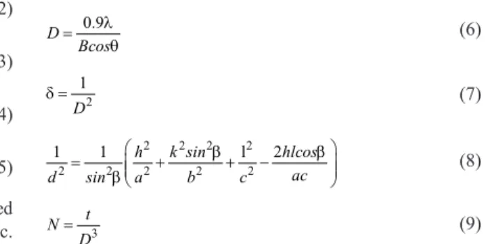
XRD patterns of the deposited ilms at different pH values are shown in Figure 1 and Table 1. The structural properties were calculated by the Scherrer formula using grain size (D), dislocation density (δ) , the number of crystallites per unit area (N), lattice parameters (205) at 10-4 M, (31-1) at 10-3 M, (002) at 10-2 M and (004) at 10-1 M planes were calculated by using the formulas given below:
0.9λ
= θ
D
Bcos (6)
2
1
δ =
D (7)
2 2 2 2
2 2 2 2 2
1 = 1 + β+l −2 β
β
h k sin hlcos
ac
d sin a b c (8)
3
= t
N
D (9)
Where t is the ilm thickness, λ is wavelength of X-ray used (1.5406 Å), β is FWHM of the peak, θ is Bragg angle, δ is dislocation density, which is deined as length of dislocation lines per unit volume of the crystal. The smallest average grain
Table 1. XRD datas of ASTM values versus ilms
Concentration ASTM Data File ASTM Value Observed Value Miller İndice
10-4 M 44-859 26.150 26.10 BiI (205)
10-3 M 44-859 27.743 27.72 BiI (31-1)
10-2 M
42-1292 11.795 11.78 Bi9I2 (-120)
73-2062 19.433 19.50 BiOI (002)
42-1292 23.669 23.61 Bi9I2 (-140)
10-445 39.366 39.42 BiOI (004)
10-445 60.695 61.08 BiOI (006)
10-1 M 73-2062 19.433 19.45 BiOI (002)
size was calculated for 0.1 M Bi and iodine concentration, at the same time the highest value of dislocation density (δ) and the number of crystallites per unit area (N) were also calculated for 0.1 M Bi and iodine concentration. On the other hand, the highest value of the average grain size was calculated for 10-3 M concentration. Similarly, the lowest value of dislocation density (δ) and the number of crystallites per unit area (N) were calculated for 10-3 M. Average grain size has been increased with the increase of Bi and I concentration, whereas average grain size has been decreased with the formation of BiOI and concentration of Bi and I has been increased. 10-2 M seems to be the threshold for the transition between BiI and BiOI structures. Change of dislocation density and number of crystallites per unit area is shown in Figure 2.
XRD analysis revealed that ilms deposited at lower concentration of bismuth and iodine had BiI structure while those deposited at higher concentration, like 10-2 M, had polycrystalline (BiOI and Bi9I2) structure. Besides that, when 0.1 M concentration of bismuth and iodine were added to the bath, BiOI structure became dominant. The XRD patterns of the BiI ilms, deposited with 10-4 M and 10-3 M concentration, indicate monoclinic structure with a preferential orientation along (205) and (31-1) directions. The peaks were detected
at 2θ = 11.78, 23.61 and 19.50, 39.42, 61.08 which can be ascribed due to (-120), (-140) and (002), (004), (006) relection planes of the monoclinic Bi9I2 and tetragonal BiOI mixed structure when 10-2 M bismuth and 10-2 M iodine were respectively added to the bath. Also, tetragonal BiOI was the dominant character in the structure when 10-1 M bismuth and Fig. 1. X-ray patterns of the ilms deposited in bath solution with: (a) 10-4 M, (b) 10-3 M, (c) 10-2 M and (d) 10-1 M concentrations.
Fig. 2. Average grain size (D), dislocation density (δ), number
10-1 M iodine were added to the bath. Under the concentration of 10-2 M bismuth and iodine, monoclinic BiI structure was observed due to (205) and (31-1) in planes. The comparison of observed and standard d-values of the thin ilms is shown in Table 1 and it is also seen that there is a good coherence between d-values. This method is very suitable for producing ilms, with BiOI and BiI structure. Patil et al., have produced hexagonal BiI3 and monoclinic BiOI via gel method by using single diffusion technique with different chemicals. According to the literature, researchers have not seen as sharp and clear peaks that we have obtained, especially with this ilm thickness and on amorphous substrates 12.
In addition, we can calculate the strains of the ilms using Williamson-Hall method:
Βhklcosθ = (kλ/D) + 4εsinθ (10)
In fact, this method is more appropriate for crystal powder rather than thin ilms. Scherrer formulas have been slightly modiied, using tanθ instead of cosθ. The aim of this method is seeking crystallization deiciencies by calculating strains or size broadenings and eventually examining the growth of the particles. In the literature, some researchers argue that this method is not adequate. The calculation is quite simple (eq. 10). The graph of Βhklcosθ vs. 4sinθ should be drawn and the slope of y = mx + c can be interpreted. Regarding our study, we can only comment about the ilms obtained from the bath with 0.01 M concentration. This is because this method requires the consideration of many diffraction peaks obtained from a measurement. However, the number of peaks that we have identiied was only 1 or 2 for the other deposition concentrations.
Film thickness of BiI and BiOI ilms were displayed in Figure 3. The thickness of the ilms was measured with AFM. Naturally, ilm structure has also shown some differences between BiI and BiOI, depending on the concentration, ilm thickness reached the maximum when 10-2 M bismuth and 10-2 M iodine were added. Then it has been decreased with the concentration increase of bath compounds. The lowest ilm thickness was measured as 98 nm with 0.1 M concentration. Zhang L. et al. produced BiOI with solvo-thermal method and the thickness of the ilms was around 5-9 µm. Our ilms were thinner than these ilms, mentioned in the literature 13.
Transmittance (T) of the thin ilm can be calculated by using relectivity (R) and absorbance (A) spectra from the expression (11):
(
)
21 −
= − A
T R e (11)
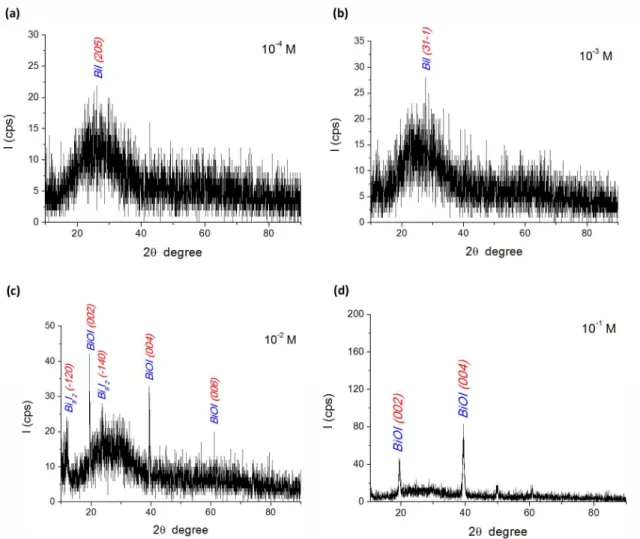
Transmission measurements are performed at room temperature at the range of 200-1100 nm , in Figure 4. The transmission curve of the ilms decreased with the increase of bismuth’s and iodine’s deposition concentrations. Only, the ilm deposited at 10-2 M concentration didn’t it this pattern. Relectivity of the ilms was inversely proportional to the transmission. However, transmission and relectivity were in line with ilm thickness. According to the literature, this kind of semi-conductor thin ilms can be used as radiation detector 8. Refractive index and extinction coeficient for the ilms are given by the formulas:
(
)
(
)
(
)
2 21 4
1 1
+
= + −
− −
R R
n k
R R
(12) 4
αλ =
k
n (13)
Refractive index was in line with deposition concentrations, which was 1.29, 1.86, 1.61 and 1.41, for 0.1-0.01-0.001-0.0001 M respectively (550 nm wavelength). Moreover, extinction coeficient behaved as refractive index and it was found to be 0.0018, 0.0106, 0.0063 and 0.0044 for 0.1-0.01-0.001-0.0001 M (550 nm wavelength in Figure 5). Refractive index and extinction coeficient were parallel to average grain size and ilm thickness. The materials having this kind of refractive index can be used in opto-electronic devices. The optical band gap energy (Eg) was determined
Fig. 3. Film thickness of the ilms.
Fig. 4. Transmittance (T) and relectivity (R) of the thin ilms at
different deposition concentrations.
from the absorption spectra of the ilms by using the following relation (14):
(
α ν =)
(
ν −)
nh A h Eg (14)
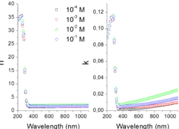
Where A is a constant, α is absorption coeficient, hν is the photon energy and n is a constant, equal to ½ for direct band gap semiconductor. The plot of (αhν)2 versus hν is presented in Figure 6.
Fig. 6. Plot of (αhυ)2 vs. hυ of the ilms at different concentrations:
(a) 10-4 M, (b) 10-3 M, (c) 10-2 M, (d) 10-1 M.
Fig. 7. SEM images of the ilms at different concentrations (a) 10-4 M, (b) 10-3 M, (c) 10-2 M, (d) 10-1 M
Band gaps (Eg) of the ilms varied between 3.50, 3.37, 3.55 and 3.67 depending on ilm thickness. Optical band gaps of the ilms were inversely proportional to average grain size and ilm thickness. The materials falling into this optical band gap range are considered as semi-conductor in the literature.
is that the structure of the ilm varied between BiI and BiOI structures according to deposition concentration. BiI structure is close to amorphous, thus they don’t have the same optical band gap as mentioned in the literature.
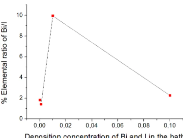
EDX technique was used to estimate the composition of the thin ilms. Fig. 8 shows the average percentage of elemental ratio of Bi/I as a function of concentration of bismuth and iodine. It was seen that Bi/I ratio changed with deposition concentration. EDX results indicate that the average atomic ratio of Bi/I is 1.80, 1.42, 9.94 and 2.25 for
0.1-0.01-0.001-0.0001 M concentrations. These results were nearly equal to the stoichiometric ratio of Bi/I at 0.1 (BiI) - 0.01 (BiI) - 0.001 (BiOI and Bi9I2) - 0.0001 (BiOI) M concentrations, which were Bi/I: 1.646 for BiI, Bi/I: 7.41 for Bi9I2 and Bi/I: 1.975 for BiOI. These results are in agreement with SEM, XRD patterns and calculations. According to literature, these ilms can be useful for gas sensing and hydrogen peroxide detection 14,15.
4. Conclusion
Bismuth iodine thin ilms were prepared via modiied CBD technique used in our previous studies16,17. The concentrations of bath compounds were changed while deposition temperature, while deposition time was kept constant. According to the literature, bismuth oxi cation has been formed in acidic media. Although is true, the concentrations of the compounds should also be considered at this point. This study clearly showed that if we can control bismuth and iodine concentrations in the acidic media, we can produce good quality BiI or BiOI ilms and we can even determine the structure of the ilm. Using chemical bath deposition method, we can easily control these parameters. Some people are aware that the concentrations of the bath affect grain size and ilm thickness. But if we can control the compounds of the bath, we can produce all types of ilm we want. These BiOI thin ilms can be useful for sensors.
Fig. 8. EDX analysis of percentage of Bi/I elements.
References
1 Warren RF. Liang,WY. Raman spectroscopy of new lead iodide
intercalation compounds. Journal of Physicis Condensed Matter.
1993;5(35):6407–6418.
2. Coleman CC, Magness B, Melo P, Goldwhite H, Tikkanen W, Tham Q. et al. Intercalation of hydrazines in lead iodide. Journal
of Physics and Chemistry of Solids. 1996;57(6-8):1153–1158.
doi:10.1016/0022-3697(95)00414-9
3. Preda N, Mihut L, Baibarac M, Baltog I, Lefrant S. A distinctive signature in the Raman and photoluminescence spectra of
intercalated PbI2. Journal of Physics: Condensed Matter.
2006;18(39):8899–8912. doi:10.1088/0953-8984/18/39/020
4. Preda N, Mihut L, Baibarac M, Baltog I, Ramer R, Pandele J,
Andronescu C, Fruth V. Films and crystalline powder of PbI2
intercalated with ammonia and pyridine. Journal of Materials
Science: Materials in Electronics. 2009;20(1):465-470. DOI
10.1007/s10854-008-9681-6
5. Schluter M, Cohen ML, Kohn SE, Fong CY. Electronic structure of BiI3. Physica Status Solidi B. 1976;73:737–747.
6. Komatsu T, Kaifu Y, Takeyama S, Miura N. Effects of high
magnetic fields on cationic exciton lines in BiI3. Physical
Review Letters. 1987;58(21):2259–2262.
7. Ghorayeb AM, Coleman CC, Yoffe AD. Giant optical band edge shifts in hydrazine-intercalated PbI2 and BiI3. Journal of
Physics C: Solid State Physics. 1984;17(27):L715–L719.
8. Garg A, Tomar M, Gupta V. Synthesis and characterisation of thin films of bismuth triiodide for semiconductor radiation detectors. In: Conference Papers in Science, 2014; 2014, Article ID 370436. 3 p. http://dx.doi.org/10.1155/2014/370436
9. Chaudhuri TK, Patra AB, Basu PK, Saraswat RS, Acharya HN. Preparation of bismuth iodide thin films by a chemical
method. Materials Letters. 1989;8(9):361-363. doi:10.1016/0167-577X(89)90008-6
10. Kodzasa T, Ushijima H, Matsuda H, Kamata T. Preparation of thin film of layer structured bismuth iodide with a long chain
alkylammonium and its nonlinear optical property. Molecular
Crystals and Liquid Crystals Science and Technology. Section
A. 2000;343:71-75. DOI: 10.1080/10587250008023505
11. Gündüz T, Yarı-Mikro KA, Kitapevi G. Kalitatif analiz: laboratuvae kitab. Hamur Kagit; Ciltsiz; 1999.
12. Patil TK, Talele MI. Comparative study of semicoductors bismuth iodate, bismuth triiodide and bismuth trisulphide crystals.
Advance Applied of Science Research. 2012;3 (3):1702-1708.
13. Zhao K, Zhang X, Zhang L. The first BiOI-based solar cells.
Electrochemistry Communication. 2009;11(3):612–615.
doi:10.1016/j.elecom.2008.12.041
14. Leontie L, Caraman M, Evtodiev I, Cuculescu E, Mija A. The anisotropy of the optical properties of ternary semiconductors
formed by elements of III and VI groups. Physica Status Solid
Applied Materials. 2008;205:2052-2056
15. Chen PY, Shih Y, Chiu MH, Zen JM, Kumar AS, Sornambikai S. Cosmetic hydrogen peroxide detection using nano bismuth species deposited built-in three-in-one screen-printed silver
electrode. International Journal of Electrochemical Science.
2011;6(7):2352-2365
16. Kariper İA. What is the effect of critical surface tension of
PbSO3 thin film?. Metallurgical and Materials Transactions
A. 2014; 45(10):4398-4404.
17. Kariper İA. Production Of HfO2 thin films using different
methods: chemical bath deposition, silar and sol-gel process.
International Journal of Minerals, Mettalurgy, and Materials.