Nuno Miguel Pinto Neves
Mestre em Engenharia de Materiais
Al-doped ZnO ceramic sputtering targets
based on nanocrystalline powders produced
by emulsion detonation synthesis
–
deposition
and application as a transparent conductive
oxide material
Dissertação para obtenção do Grau de Doutor
em Ciência e Engenharia de Materiais
Orientador: Doutora Isabel Maria das Mercês Ferreira,
Professora Associada, Faculdade de Ciências e
Tecnologia
–
Universidade Nova de Lisboa
Co-orientador: Doutora Ana Lúcia Lagoa, Investigação e
Desenvolvimento de Nanomateriais,
INNOVNANO
–
Materiais Avançados, SA
Júri:
Presidente: Professora Doutora Maria Luísa Dias de Carvalho de Sousa Leonardo Arguentes: Professora Doutora Paula Maria Lousada Silveirinha Vilarinho
Professor Doutor Carlos José de Macedo Tavares
Vogais: Professor Doutor Albano Augusto Cavaleiro Rodrigues de Carvalho Professora Doutora Elvira Maria Correia Fortunato
Professora Doutora Regina da Conceição Corredeira Monteiro Professora Doutora Olinda Maria Quelhas Fernandes Conde
i
Nuno Miguel Pinto Neves
Mestre em Engenharia de Materiais
Al-doped ZnO ceramic sputtering targets
based on nanocrystalline powders produced
by emulsion detonation synthesis
–
deposition
and application as a transparent conductive
oxide material
Dissertação para obtenção do Grau de Doutor
em Ciência e Engenharia de Materiais
Orientador: Doutora Isabel Maria das Mercês Ferreira,
Professora Associada, Faculdade de Ciências e
Tecnologia
–
Universidade Nova de Lisboa
Co-orientador: Doutora Ana Lúcia Lagoa, Investigação e
Desenvolvimento de Nanomateriais,
INNOVNANO
–
Materiais Avançados, SA
Júri:
Presidente: Professora Doutora Maria Luísa Dias de Carvalho de Sousa Leonardo Arguentes: Professora Doutora Paula Maria Lousada Silveirinha Vilarinho
Professor Doutor Carlos José de Macedo Tavares
Vogais: Professor Doutor Albano Augusto Cavaleiro Rodrigues de Carvalho Professora Doutora Elvira Maria Correia Fortunato
Professora Doutora Regina da Conceição Corredeira Monteiro Professora Doutora Olinda Maria Quelhas Fernandes Conde
iii Al-doped ZnO ceramic sputtering targets based on nanocrystalline powders produced by emulsion detonation synthesis – deposition and application as a transparent conductive oxide material
Copyright: Nuno Miguel Pinto Neves FCT/UNL e UNL
Acknowledgments
v
Acknowledgments
This thesis is a result of about five years of hard work, during which for sure I learnt a lot, from both professional and personal point of view. Besides the personal effort made during countless days and nights of work, when I think back and look around there are a number of people without whom this thesis might have not be written, and to whom I am greatly indebted.
First and foremost, I would like to express my sincere gratitude to my supervisor Professor Isabel Ferreira, for providing me the privilege to work with her in this project, for the form she guided my work with their knowledge and singular enthusiasm, for their support and encouragement, for all the suggestions and “crazy ideas”, for their friendship and patience, and of course for the countless long talks held in the late afternoon. Thank you for everything.
To my friend and supervisor in Innovnano Dr. Ana Lagoa, for all the support in the company throughout this years, for many scientific discussions and for being always available to help professionally and personally. Without her knowledge, ideas and advices, this work would not have taken the same direction.
To Professor Rodrigo Martins and Professor Elvira Fortunato, for allowing me to work in this prestigious research group during these years, for their support, incentive and fellowship. Even having developed large part of the work out of the research center, they always made me feel like
“part of the group”. Thank you for the confidence in me and my work.
To CUF group where Innovnano is incorporated, for investing in my professional and personal development. To Dr. André de Albuquerque and Eng. João Calado I express my sincere thanks for the opportunity to take this project to the end. It is gratifying and I am proud to be part of CUF group.
To Dr. Raquel Barros, a special and grateful thank. Without her friendly help in the clean chamber and on the characterization of the thin films this work would not have been possible. Thanks for the good times we spent together, for never having said no to the “crazy schedules” that I proposed to work, for your endless patience, and for our Sushi sessions! You are a good friend! To Eng. Ana Casaca for the support in terms of the company intellectual property management and for making easy what is commonly complicated.
To Professor Pedro Mantas, for the few but always motivating and interesting conversations. Their personal advices were essential.
To Eng. Sílvio Pratas, which more than a co-worker at Innovnano is a great friend. Thanks for all the good moments over these years and for teaching me to enjoy a good Alentejo wine.
To my colleagues and co-workers in Innovnano, MSc. Sofia Soares, MSc. Marisa Rodrigues and MSc. Cristina Mesquita, for the friendship, professional and personal support. Thank you very much!
vi
To Dr. Andrei Galatanu from the National Institute of Materials Physics in Romania for the thermal measurements, availability and knowledge sharing.
To the Centre for Renewable Energy Systems Technology (CREST), namely to Professor John Walls, DR. Jake Bowers and MSc. Patrick Isherwood for the scientific talks and the work developed together in AZO thin films.
To MSc. Rosa Calinas for the SEM and TEM analyses performed in the University of Texas at Austin.
To Eng. Ana Bicho from Solarplus, for providing their manufacturing facilities for the tests with the industrial ceramic targets.
To professor Ana Rego, for the XPS measurements and characterization done at IST.
To Professor Jorge Frade, for providing his lab over these years for the preparation of CIP samples. To Professor Jorge Saraiva and MSc. Rui Queirós from DQUA, for the uncountable CIP tests performed in their facilities.
To past and present co-workers in CENIMAT and DCM that, direct or indirectly, contributed to this work: Professor Pedro Barquinha, Professor Luis Pereira, Professor Teresa Cidade, MSc. Sónia Pereira, MSc. Alexandra Gonçalves, MSc Mafalda Costa, Dr. Joana Loureiro, MSc. Paulo Duarte, Dr. Ana Baptista, Dr. Rita Braquinho, MSc. Lídia Santos, Dr. Joana Vaz Pinto, Msc. Diana Gaspar, Msc. Andreia Araújo, MSc. António Vicente, Dr. Iwona Wojcik, Dr. Pawel Wojcik, Dr. Ana Pimentel, Dr. Daniela Nunes, Dr. Sergey Filonovich, MSc. Jonas Duermeier, Dr. Tito Busani, Msc. Tiago Mateus, Dr. Elangovan Elamurugu, Eng. Nuno Correia, Dr. Vitor Figueiredo, and others that probably I did not mention. Your help was essential Thank you all!
To all co-workers of Innovnano not mentioned above, which direct or indirectly helped me in this journey.
For all the true moments of friendship and fun, I must thank to my longtime friends César Esteves, Eduardo Arvins, José Pedro, Bruno Tiago, Vitor Oliveira, Luís Pereira and Pedro Moreira. Everything is turned much easier having friends like them in our side.
To all my family, especially to my brother Hugo for being my best friend and an example for me, my nieces Beatriz and Inês for their special hugs and for being my princesses, my grandparents Virgílio and Fátima, two people with a huge heart, my uncle Virgílio for being a “second father”, and to the most important persons in my life: my parents Fernando and Virginia for their love and comprehension, for devoting their life to give me the best anyone could have. I own them all that I am today and no words ever be enough to thank them!
Abstract
vii
Abstract
Transparent conducting oxides (TCOs) have been largely used in the optoelectronic industry due to their singular combination of low electrical resistivity and high optical transmittance. They are usually deposited by magnetron sputtering systems being applied in several devices, specifically thin film solar cells (TFSCs). Sputtering targets are crucial components of the sputtering process, with many of the sputtered films properties dependent on the targets characteristics.
The present thesis focuses on the development of high quality conductive Al-doped ZnO (AZO) ceramic sputtering targets based on nanostructured powders produced by emulsion detonation synthesis method (EDSM), and their application as a TCO. In this sense, the influence of several processing parameters was investigated from the targets raw-materials synthesis to the application of sputtered films in optoelectronic devices.
The optimized manufactured AZO targets present a final density above 99 % with controlled grain size, an homogeneous microstructure with a well dispersed ZnAl2O4 spinel phase, and electrical resistivities of ~4 × 10⁻⁴ Ωcm independently on the Al-doping level among 0.5 and 2.0 wt. % Al2O3. Sintering conditions proved to have a great influence on the properties of the targets and their performance as a sputtering target. It was demonstrated that both deposition process and final properties of the films are related with the targets characteristics, which in turn depends on the initial powder properties.
In parallel, the influence of several deposition parameters in the film´s properties sputtered from these targets was investigated. The sputtered AZO TCOs showed electrical properties at room temperature that are superior to simple oxides and comparable to a reference TCO – indium tin oxide (ITO), namely low electrical resistivity of 5.45 × 10⁻⁴Ωcm, high carrier mobility (29.4 cm2V-1s -1), and high charge carrier concentration (3.97
× 1020 cm-3), and also average transmittance in the visible region > 80 %. These superior properties allowed their successful application in different optoelectronic devices.
Resumo
ix
Resumo
Os óxidos condutores transparentes (TCOs) têm sido amplamente utilizados na indústria optoelectrónica devido à combinação única de baixa resistividade eléctrica e elevada transmitância óptica. São geralmente depositados por pulverização catódica assistida por magnetrão em inúmeros dispositivos, especificamente células solares de filme fino (TFSCs). Os alvos para deposição catódica são componentes cruciais no processo de pulverização, com muitas das propriedades dos filmes pulverizados a dependerem das características dos alvos.
Esta tese de doutoramento foca o desenvolvimento de alvos cerâmicos condutores de óxido de zinco dopado com alumínio (AZO) de elevada qualidade para deposição catódica, a partir de pós nanoestruturados produzidos pelo método de síntese por detonação de emulsão (EDSM). Para tal, foi investigada a influência dos diversos parâmetros de processamento desde a síntese dos pós usados no fabrico dos alvos até à aplicação dos filmes pulverizados em dispositivos optoelectrónicos.
Os alvos de AZO optimizados apresentam uma densidade final superior a 99 % com um tamanho de grão controlado, uma microestrutura homogénea com uma fase espinela ZnAl2O4 bem distribuída, e resistividades eléctricas de ~4 × 10⁻⁴Ωcm independentemente da quantidade de Al como dopante no intervalo 0.5 – 2.0 % em peso de Al2O3. As condições de sinterização demonstram ter um efeito preponderante nas propriedades finais dos alvos e na sua performance como alvo de deposição catódica. Foi demonstrado que tanto o processo de deposição como as propriedades dos filmes estão correlacionados com as características dos alvos, que por sua vez dependem das propriedades do pó inicial.
Em paralelo, foi estudada a influência de diversos parâmetros de deposição nas propriedades dos filmes depositados com esses alvos. Os TCOs de AZO pulverizados apresentam propriedades eléctricas à temperatura ambiente superiores às dos óxidos binários e comparáveis com um TCO de referência – óxido de índio dopado com estanho (ITO), nomeadamente baixa resistividade eléctrica, (5.45 × 10⁻⁴ Ωcm), elevada mobilidade (29.4 cm2V-1s-1), elevada concentração de portadores de carga (3.97 × 1020 cm-3), e ainda uma transmitância média no visível superior a 80 %. Estas propriedades permitiram a aplicação com sucesso destes filmes em diferentes dispositivos optoelectrónicos.
Table of contents
xi
Table of contents
Chapter 1. Motivation, objectives, and structure of the dissertation ...1
1.1.
Motivation
... 11.2.
Objectives
...
21.3.
Structure of the dissertation
...
21.4.
References
...
4Chapter 2. Introduction ...5
2.1.
Nanotechnology and nanomaterials
... 52.1.1. Global market trends ... 5
2.2.
Overview of nanoparticles synthesis technologies
... 62.2.1. Solid phase synthesis methods ... 7
2.2.1.1. Mechanical milling ... 7
2.2.1.2. Solid-vapor synthesis ... 8
2.2.1.3. Solid-state reactions ... 8
2.2.2. Liquid-phase synthesis methods ... 9
2.2.2.1. Chemical precipitation synthesis ... 9
2.2.2.2. Sol-gel synthesis method...10
2.2.3. Gaseous-phase synthesis methods ...11
2.2.3.1. Combustion synthesis ...12
2.2.3.2. Thermal plasma synthesis ...12
2.3.
INNOVNANO
–
Novel emulsion detonation synthesis method
...132.3.1. Overview of the company – research areas and future prospects ...14
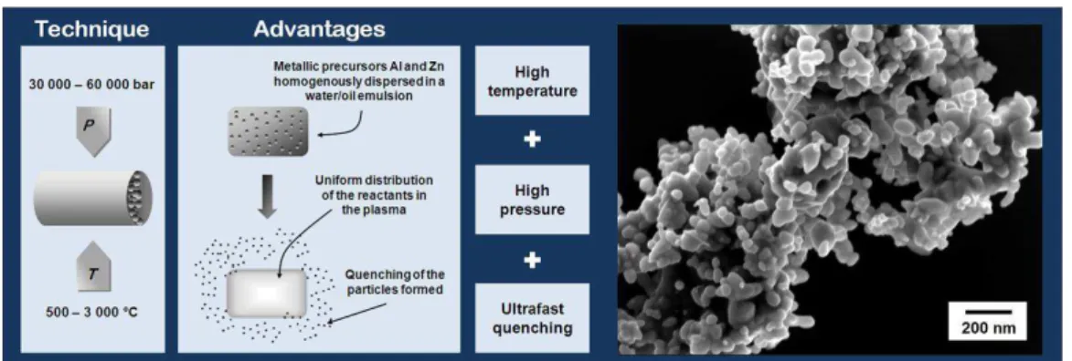
2.3.2. Emulsion detonation synthesis method ...15
2.3.2.1. Emulsion detonation synthesis versus competitor´s synthesis methods ...18
2.4.
Synthesis of aluminum-doped zinc oxide nanoparticles
...212.5.
Transparent conductive oxides (TCOs)
...222.5.1. History – Past, present and future of TCOs ...23
2.5.2. General properties of TCOs ...24
2.5.2.1. Theoretical approaches and limitations over TCOs electrical and optical properties ...26
2.5.3. Most commonly used TCOs – trends, limitations and future perspectives ...28
2.5.3.1. Undoped and Sn-doped In2O3 (ITO) thin films ...29
2.5.3.2. Undoped and Al-doped ZnO (AZO) thin films ...31
2.6.
Global market of sputtered TCO thin films and sputtering targets
...36xii
2.7.1. AZO ceramic sputtering targets ... 40
2.7.1.1. Consolidation techniques ... 41
2.7.1.2. Raw materials ... 41
2.7.1.3. Oxygen content – Influence of sintering atmosphere ... 42
2.7.1.4. Thermal and mechanical properties ... 43
2.8.
Correlation between AZO ceramic sputtering targets and sputtered thin films
432.9.
Processing of nanosized ceramic powders
... 452.10. Sintering
–
Basic concepts
... 462.11. Solid state sintering
... 472.11.1. Driving force for sintering ... 47
2.11.2. Mechanisms of transport in the initial stage of sintering ... 49
2.11.3. Mechanisms of transport in the intermediate and final stages of sintering ... 51
2.11.4. Stages of sintering ... 53
2.11.5. Grain growth ... 54
2.11.6. Particle size effect ... 55
2.11.7. Pressure-assisted sintering ... 56
2.11.7.1.Driving force of pressure-assisted sintering and inherent sintering mechanisms ... 57
2.12. Undoped ZnO
–
Sintering and densification
... 572.13. Al-doped ZnO
–
Sintering and densification
... 592.14. References
... 61Chapter 3. Experimental details ... 71
3.1.
Powder: Synthesis and characterization techniques
... 713.1.1. Synthesis... 71
3.1.2. Subsequent processing stages – thermal treatment, deagglomeration and drying . 73 3.1.3. Characterization techniques ... 74
3.1.3.1. Particle and granule size distribution – CPS and Malvern ... 74
3.1.3.2. Dilatometry tests ... 75
3.1.3.3. Structural and morphological characterization ... 76
3.1.3.3.1. X-ray diffraction (XRD)... 76
3.1.3.3.2. True density – Gas pycnometry ... 77
3.1.3.3.3. Specific surface area (SSA) ... 78
3.1.3.3.4. Scanning electron microscopy (SEM) ... 79
3.1.3.3.5. Transmission electron microscopy (TEM) ... 80
Table of contents
xiii 3.1.3.4.1. Differential scanning calorimetry/Thermo-gravimetric analysis
(DSC/TGA) ...81
3.1.3.5. Compositional characterization ...82
3.1.3.5.1. Energy-dispersive X-ray spectroscopy (EDS)...82
3.1.3.5.2. X-ray fluorescence (XRF) ...83
3.1.3.5.3. X-ray photoelectron spectroscopy (XPS) ...84
3.2.
Ceramic targets: Production and characterization techniques
...853.2.1. Ceramic targets production ...85
3.2.1.1. Preparation of powder compacts ...85
3.2.1.2. Consolidation techniques ...86
3.2.1.2.1. Conventional sintering ...86
3.2.1.2.2. Hot-pressing sintering (HP) ...86
3.2.1.2.3. Spark plasma sintering (SPS) ...87
3.2.1.3. Density measurement ...88
3.2.1.4. Polishing ...88
3.2.2. Characterization techniques ...89
3.2.2.1. Structural and morphological characterization ...89
3.2.2.1.1. X-ray diffraction (XRD) ...89
3.2.2.1.2. Scanning electron microscopy (SEM) – grain size measurement ...89
3.2.2.2. Compositional characterization ...90
3.2.2.2.1. Auger electron spectroscopy (AES) ...90
3.2.2.3. Electrical characterization ...90
3.2.2.4. Thermal characterization ...92
3.2.2.5. Mechanical characterization ...93
3.2.2.5.1. Vickers hardness and fracture toughness ...93
3.2.2.5.2. Biaxial flexural strength ...94
3.3.
Thin films: deposition and characterization techniques
...953.3.1. Thin films deposition ...95
3.3.1.1. Sputtering ...95
3.3.2. Characterization techniques ...100
3.3.2.1. Structural and morphological characterization ...100
3.3.2.1.1. X-ray diffraction (XRD) ...100
3.3.2.1.2. Scanning electron microscopy (SEM) ...101
3.3.2.1.3. Profilometry...101
3.3.2.1.4. Atomic force microscopy (AFM) ...102
3.3.2.2. Compositional characterization ...102
3.3.2.3. Optical characterization ...103
xiv
3.3.2.4. Electrical characterization ... 104
3.4.
References
... 105Chapter 4. Powder: Synthesis and characterization ... 107
4.1.
Particle size effect on sintering behavior of undoped ZnO
... 1074.1.1. Commercial ZnO powder characterization ... 108
4.1.1.1. Constant heating rate sintering analysis – densification behavior ... 109
4.1.1.1.1. Effect of green density ... 109
4.1.1.1.2. Influence of heating rate ... 111
4.1.1.1.3. Activation energy and sintering mechanisms in the initial stage ... 111
4.1.1.1.4. Densification and grain growth ... 112
4.1.1.1.5. Scale-up effect ... 115
4.2.
Undoped and Al-doped ZnO powders by emulsion detonation synthesis
... 1164.2.1. Powder synthesis – precursors ... 116
4.2.2. Powder characterization ... 119
4.2.2.1. Chemical composition analysis ... 120
4.2.2.2. Structural analysis ... 122
4.2.2.3. Morphological analysis ... 123
4.2.2.4. Processing stages – Thermal treatment ... 125
4.2.2.5. Processing stages – Disaggregation/deagglomeration ... 126
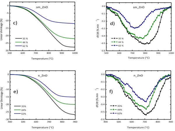
4.2.3. Constant heating rate sintering analysis ... 129
4.2.3.1. Densification behavior ... 129
4.2.3.2. Activation energy and sintering mechanisms in the initial and intermediate stages ... 131
4.3.
Conclusions
... 1334.4.
References
... 135Chapter 5. AZO ceramic sputtering targets and sputtered thin films:
production and characterization ... 137
5.1.
Conventional sintering
... 1375.1.1. Green density effect on sintering ... 138
5.1.2. Grain growth ... 142
5.1.3. Structural characterization ... 143
5.1.4. Morphological characterization ... 144
5.1.5. Effect of aluminum doping concentration ... 144
5.1.5.1. Densification ... 145
Table of contents
xv
5.1.5.2.1. Dragging effect of ZnAl2O4 spinel phase on grain growth ...149
5.1.5.3. Solubility limit of Al-doped ZnO and spinel phase formation ...151
5.1.6. Electrical properties of AZO ceramic sputtering targets produced by CS ...154
5.1.6.1. Structural and microstructural effect ...154
5.1.6.2. Effect of aluminum doping concentration ...157
5.1.6.3. Scale-up effect ...160
5.1.7. AZO thin films sputtered from conventionally sintered sputtering targets – deposition and characterization ...161
5.1.7.1. Deposition rate of Al-doped ZnO thin films ...161
5.1.7.2. Effect of RF-sputtering power on AZO thin films properties ...162
5.1.7.3. Effect of deposition pressure on AZO thin films properties ...166
5.1.7.4. Effect of Al-doping concentration on AZO thin films properties ...169
5.1.7.4.1. Solubility limit of Al in ZnO sputtered thin films ...172
5.1.8. Effect of sintering atmosphere during CS ...173
5.1.8.1. Influence of sintering atmosphere on target properties ...174
5.1.8.2. Sputtering of Ar sintered targets and their film properties ...177
5.2.
AZO sputtering targets manufacture
–
Alternative methods and its effects on
sputtered thin films
...1785.2.1. AZO sputtering targets by hot-pressing (HP) ...178
5.2.1.1. Hot-pressed AZO targets – manufacturing and characterization ...179
5.2.1.2. Sputtering of hot-pressed AZO targets and their film properties ...182
5.2.1.2.1. Properties of AZO films sputtered from hot-pressed 2” AZO targets ...183
5.2.1.2.2. Properties of AZO films sputtered from hot-pressed 3” AZO target – effect of substrate temperature during deposition ...184
5.2.2. AZO sputtering targets by spark-plasma-sintering (SPS) ...190
5.2.2.1. Processing conditions and targets characterization ...190
5.2.2.2. Thin films – deposition and characterization ...192
5.2.3. Non-sintered AZO sputtering targets – thin films deposition and characterization ...193
5.2.3.1. Effect of deposition pressure on AZO thin films properties ...194
5.2.3.2. Effect of film thickness on AZO thin films properties ...196
5.2.3.3. Deposition rate of Al-doped ZnO thin films ...200
5.2.3.4. Application of AZO thin films to a-Si:H tandem solar cells and GIZO thin film transistors ...201
5.2.3.4.1. Devices – fabrication and characterization ...203
5.3.
Application of AZO thin films as a thermoelectric material
...207xvi
5.3.2. Properties of AZO TE-TF – Effect of composition, thickness, sputtering target and
deposition method ... 208
5.4.
Correlation between electrical resistivity, carrier concentration and mobility of
the carriers
–
physical limits and active scattering mechanisms in sputtered
AZO thin films
... 2125.5.
Compositional analysis of AZO targets and sputtered films
... 2165.6.
Thermal and mechanical properties of AZO targets
... 2195.6.1. Thermal properties... 220
5.6.2. Mechanical properties ... 222
5.7.
Industrial scale-up
–
manufacturing of large size AZO sputtering targets and its
application as a TCO in thin film solar cells
... 2235.7.1. Atomization ... 224
5.7.2. Uniaxial pressing of the green compacts ... 225
5.7.3. Sintering, machining and bonding of the targets ... 226
5.7.4. Application as a TCO material in commercial a-Si:H TFSCs ... 227
5.7.5. Arcing and nodules formation during sputtering ... 231
5.8.
AZO targets available
–
market position of INNOVNANO
... 2335.9.
Conclusions
... 2375.10. References
... 242Chapter 6. Final conclusions and further work ... 249
6.1.
Final conclusions
... 249List of figures
xvii
List of figures
Fig. 1.1. Examples of transparent electronics applications – From left to right: Semi-transparent a-Si:H thin film solar cell deposited on glass substrate and Samsung mobile phone with flexible and
transparent 4.3’’ AMOLED display [1]). ... 1 Fig. 2.1. Global nanotechnology market, 2009 – 2017 (US $ millions) (Adapted from [4] and [5])... 6 Fig. 2.2. Overview of the main manufacturing methods for metal-oxide nanoparticles (Adapted from [2]). ... 7 Fig. 2.3. Main steps of chemical precipitation synthesis method for the production of
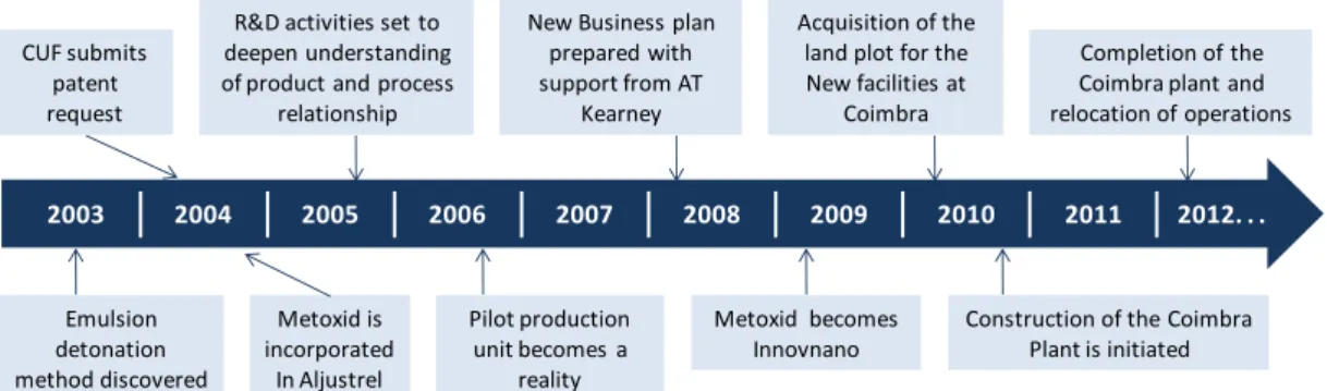
nanoparticles (Adapted from [2]). ...10 Fig. 2.4. Schematic illustration of a combustion synthesis process (adapted from [60]). ...12 Fig. 2.5. Schematic view of a plasma evaporation process (adapted from [61]). ...13 Fig. 2.6. Some important dates since the discovery of EDSM in 2003 until the beginning of
industrial production in INNOVNANO plant (2012). ...14 Fig. 2.7. INNOVNANO production plant built in Coimbra (Portugal) in 2012. ...15 Fig. 2.8. Schematic presentation of INNOVNANO emulsion detonation synthesis process. ...15 Fig. 2.9. (P,T) phase diagram of a pure substance showing the two routes leading to a
supersaturated vapour state: (1) isobaric cooling, (2) isothermal compression (adapted
from [61]). ...16 Fig. 2.10. General conditions for transparent conducting materials: i) bandgap higher than 3 eV; ii) carrier concentration below 1021 cm-3 (adapted from [86]). ...22 Fig. 2.11. Bands diagram representation of the Burstein-Moss effect (adapted from [122]). ...28 Fig. 2.12. Cubic crystalline structure (bixbyite) of In2O3. The large spheres represent the In metallic cations (dark and light blue spheres illustrate the two distinct positions of In in the unit cell), while the small green spheres represent oxygen anions. ...29 Fig. 2.13. Bands diagram of ITO with different doping levels (Adapted from [122]). ...31 Fig. 2.14. Hexagonal crystalline structure (wurtzite) of ZnO. The large dark blue spheres represent the Zn metallic cations, while the small green spheres represent the oxygen anions. ...32 Fig. 2.15. Typical point defects observed in intrinsically doped ZnO – a) Oxygen vacancy (VO), and b) Zn2+ in an interstitial position (Zni). ...33 Fig. 2.16. Schematics of the conduction mechanisms in extrinsically doped ZnO – a) Al3+ occupying a Zn2+ site in the ZnO lattice, and b) Al3+ occupying adjacent sites. ...35 Fig. 2.17. Schematic Brouwer diagram (log concentration versus log pO2) for ZnO:Al (AZO). Vertical dotted line separates different electroneutrality regimes. Fractions indicate line slopes, n
xviii
Fig. 2.20. Thin film solar cells market share by technology type between 2005 and 2020 (adapted
from [190]). ... 38
Fig. 2.21. Global market for sputtered films and sputtering targets in 2011 and forecast for 2016 (adapted from [191]). ... 39
Fig. 2.22. Examples of ITO (left) and AZO (right) industrial planar and rotary ceramic targets produced by Umicore [196]. ... 40
Fig. 2.23. Electrical resistivity as a function of oxygen content in AZO ceramic targets (adapted from [192]) ... 43
Fig. 2.24. Oxygen content of AZO thin films as a function of oxygen content in targets (adapted from [192]). ... 45
Fig. 2.25. Schematic presentation of agglomerated and aggregated powders (adapted from [219]). ... 46
Fig. 2.26. Basic phenomena occurring during sintering under the driving force for sintering, ∆(γA)(adapted from [228]). ... 47
Fig. 2.27. Two-particle models for initial sintering stage: a) without shrinkage, b) with shrinkage (adapted from [225]). ... 48
Fig. 2.28. Migration of atoms and vacancies due to the difference in chemical potential (adapted from [227]). ... 49
Fig. 2.29. Schematic representation of the material transport paths during sintering and corresponding sintering mechanisms (adapted from [228]). ... 50
Fig. 2.30. Schematic showing the densification curve of a powder compact and the three sintering stages (adapted from [228]). ... 53
Fig. 3.1. Schematic presentation of INNOVNANO synthesis process – Nanocrystalline ceramic AZO powder formation. ... 73
Fig. 3.2. Nano bead mill DISPERMAT® SL-nano from VMA available at INNOVNANO. ... 73
Fig. 3.3. CPS Disc centrifuge – Model DC 20000 and Malvern Mastersizer 2000 equipments existing at INNOVNANO. ... 74
Fig. 3.4. Linseis L-75 Platinum Series vertical dilatometer available at INNOVNANO ... 75
Fig. 3.5. Schematic representation of Bragg´s Law (left) and Bruker D8 Advance X-ray diffractometer available at INNOVNANO (right). ... 77
Fig. 3.6. Accupyc II 1340 picnometer from Micrometrics available at INNOVNANO... 77
Fig. 3.7. Quantachrome Nova 1000E Series equipment existing at INNOVNANO. ... 79
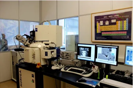
Fig. 3.8. Zeiss Auriga CrossBeam SEM-FIB system available at CENIMAT/I3N. ... 80
Fig. 3.9. JEOL 2010 F transmission electron microscope (TEM) existing at the Center for Nano and Molecular Science – University of Texas. ... 81
Fig. 3.10. NETZSCH STA 449 F3 Jupiter® DSC-TGA equipment available at CENIMAT/I3N. ... 82
Fig. 3.11. Typical example of an EDS spectrum. ... 82
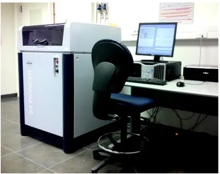
Fig. 3.12. Bruker-AXS S4 Pioneer X-ray Fluorescence Spectrometer available at INNOVNANO. .... 83
List of figures
xix Fig. 3.14. Hot-pressing sintering diagram (adapted from [31])...87 Fig. 3.15. Spark plasma sintering diagram (adapted from [34]). ...87 Fig. 3.16. Schematic presentation of the van der Pauw configuration used for Hall effect
xx
Fig. 4.13. a) EDS recorded from the circular region presented in b); b) TEM image of as-produced Al-doped ZnO powder (AZO_PM)... 118 Fig. 4.14. SEM images showing the sheet-like nanostructured AZO powder (98:2 wt. %)
synthesized by EDS using acetates as precursors. ... 118 Fig. 4.15. SEM photograph showing the general morphology of as-produced Al-doped ZnO
powders. ... 119 Fig. 4.16. a) X-ray photoelectron spectroscopy (XPS) survey spectra of as-produced AZO_D powder sample; b) Zn 2p3/2, c) Al 2p and d) O 1s XPS regions. ... 121 Fig. 4.17. X-ray diffraction patterns of undoped and Al-doped ZnO powders synthesized by EDSM. Insets showing gahnite (ZnAl2O4) as a secondary phase present in the as-produced AZO
powders ... .122 Fig. 4.18. a) SEM and b) TEM images of Al-doped ZnO (2.0 wt. % Al2O3) nanostructured powder, c) typical size distribution (in number) of the particles accordingly to SEM and TEM analysis (Inset shows the equivalent diameter derived from the particles volume fraction), d) HRTEM image and the inset with the SAED pattern of the single-crystalline particle. ... 123 Fig. 4.19. Morphology and composition of AZO_D nanostructured powder after thermal
treatment at 600 °C for 2 h. TEM bright-field image of some agglomerated AZO particles and mapping acquired by EDS in STEM showing distributions of Zn, O and Al. ... 124 Fig. 4.20. Specific surface area (SSA) and crystallite size of AZO_D (2.0 wt. % Al2O3) nanostructured powder versus thermal treatment temperature. The powders were thermally treated in the range of 300 °C – 900 °C for 2 h in air with a constant heating/cooling rate of 10 °C.min-1. ... 125 Fig. 4.21. Variation of (a) specific surface area (SSA) and (b) crystallite size of AZO_D (2.0 wt. % Al2O3) nanostructured powder with holding time. The powders were thermally treated in the range of 500 – 650 °C for 1 – 8 h in air with a constant heating/cooling rate of 10 °C.min-1. ... 126 Fig. 4.22. PSD (weight fraction) of Al-doped ZnO 98:2 wt% powders before (AZO_BD) and after disaggregation (AZO_AD) stage. The dashed lines represent the cumulative curves (in percentage of relative weight) of each powder. ... 127 Fig. 4.23. XRD diffraction of Al-doped ZnO 98:2 wt% powders before (AZO_BD) and after
List of figures
xxi Fig. 5.1. Variation of density versus compaction pressure for as-pressed AZO_D (GD) and AZO_D sintered at 1150°C for 2 h. ...139 Fig. 5.2. Influence of sintering temperature and GD on ρr of AZO_D powder (98:2 wt. %
ZnO:Al2O3) at a CHR of 5 °C.min-1. ...140 Fig. 5.3. Weight loss of AZO_D samples as a function of a) sintering temperature (1100 – 1450 °C) and b) HT (2 – 16 h). ...140 Fig. 5.4. Influence of HT and GD at a) 1100 °C, b) 1150 °C and c) 1200 °C on ρr of INNOVNANO AZO_D powder (98:2 wt. % ZnO:Al2O3). ...141 Fig. 5.5. Relative density and grain size of Al-doped ZnO (98:2 wt. %) compacts sintered at
different temperatures and a constant holding times. ...142 Fig. 5.6. X-ray diffraction patterns of AZO 98:2 wt. % ceramic targets (62 % GD) at RT (left)
showing wurtzite as the main phase of AZO targets; Detail illustrating the ZnAl2O4 spinel phase peak with HT and sintering temperature (right). ...143 Fig. 5.7. SEM micrographs of Al-doped ZnO 98:2 wt. % samples sintered for 2 h at: a) 1100 °C, b) 1200 °C, c) 1300 °C and d) 1400 °C...144 Fig. 5.8. Effect of aluminum content (0.5 – 2.0 wt. % Al2O3) on 𝜌𝑟 of Al-doped ZnO compacts sintered at different temperatures and a constant HT of 2 h. ...145 Fig. 5.9. Influence of HT and aluminum content (0.5 – 2.0 wt. % Al2O3) on ρr of Al-doped ZnO compacts sintered at a) 1050 °C, b) 1100 °C and c) 1150 °C respectively. ...146 Fig. 5.10. Effect of aluminum content (0.5 - 2.0 wt. % Al2O3) on grain size of AZO compacts
xxii
Fig. 5.21. Electrical resistivity, carrier concentration and Hall mobility of AZO thin films as a
function of 𝑃𝑅𝐹 deposited at an Ar pressure of 0.2 Pa. ... 163 Fig. 5.22. XRD patterns of AZO_D films deposited at RT as a function of 𝑃𝑅𝐹(the diffractograms are normalized to the thickness of each film). ... 164 Fig. 5.23. a) AZO films morphology and b) cross-section structure, deposited at RT (𝑃𝑅𝐹= 250 W; 𝑃𝑑𝑒𝑝= 0.2 Pa). ... 164 Fig. 5.24. RMS roughness of the AZO thin films as a function of RF power. ... 165 Fig. 5.25. Optical transmittance spectra for AZO_D films sputtered with different RF powers (𝑃𝑑𝑒𝑝= 0.2 Pa). The inset shows the variation in optical band gap energy at different RF power. 166 Fig. 5.26. Electrical resistivity, carrier concentration and Hall mobility of AZO thin films as a
function of 𝑃𝑑𝑒𝑝 deposited at an RF power of 250 W. ... 167 Fig. 5.27. XRD patterns of AZO_D films deposited at RT as a function of 𝑃𝑑𝑒𝑝(the diffractograms are normalized to the thickness of each film). ... 168 Fig. 5.28. Optical transmittance as a function of wavelength for AZO_D films sputtered at different working pressures (𝑃𝑅𝐹= 250 W). The inset shows the variation in 𝐸𝑜𝑝𝑡 energy with the working pressure. ... 168 Fig. 5.29. Effect of target doping concentration on electrical resistivity, Hall mobility and carrier concentration of AZO thin films deposited at RT (𝑃𝑅𝐹 = 250 W; 𝑃𝑑𝑒𝑝 = 0.2 Pa). ... 169 Fig. 5.30. XRD patterns of Al-doped ZnO films deposited at RT as a function of aluminum
concentration (the diffractograms are normalized to the thickness of each film). ... 171 Fig. 5.31. AZO films morphology as a function of aluminum concentration deposited at RT ((𝑃𝑅𝐹 = 250 W; 𝑃𝑑𝑒𝑝 = 0.2 Pa). ... 171 Fig. 5.32. Optical transmittance of Al-doped ZnO films with the doping concentration. The inset shows the variation in optical bandgap. ... 172 Fig. 5.33. a) Relative density and b) grain size dependence on sintering temperature and
composition for AZO samples sintered in Ar atmosphere (𝑃𝑂2~ 10-5 atm). ... 174 Fig. 5.34. Microstructural analysis showing the typical morphology of INNOVNANO AZO ceramic targets with different aluminum contents sintered at 1300 °C with 2 h of HT under Ar
atmosphere. ... 175 Fig. 5.35. X-rays diffraction patterns of AZO ceramic targets (1300 °C and 2 h of HT) with 0.5 and 2.0 wt. % Al2O3 sintered in Ar atmosphere. ... 175 Fig. 5.36 a) Transmittance spectra and b) XRD pattern of AZO thin film deposited at RT from the AZO target (98:2 wt. % ZnO:Al2O3) sintered in Ar atmosphere (𝑃𝑅𝐹= 250 W; 𝑃𝑑𝑒𝑝= 0.2 Pa). ... 177 Fig. 5.37.Picture of the 3” and 2” hot-pressed targets with an Al-doping concentration of 0.5 wt. % Al2O3 (targets sintered at 1025 °C for 1h)... 180 Fig. 5.38. TEM sample thinned to 75 nm by FIB milling using a dual beam FEI Nova 600 Nanolab SEM a) and SEM b) images of the AZO target material sintered by HP at 1025 °C for 1 h at a
List of figures
xxiii Fig. 5.40.SEM image of the polished surface of 2” AZO target (2.0 wt. % Al2O3) without thermal etching. ...181 Fig. 5.41.Picture of the 3” hot-pressed AZO target with an Al-doping concentration of 0.5 wt. % Al2O3 bonded to a cooper support. ...183 Fig. 5.42. a) Transmittance spectra and b) XRD pattern of AZO thin films deposited at RT from the 98:2 wt.% and 99.5:0.5 wt.% AZO targets prepared by HP (𝑃𝑅𝐹= 250 W; 𝑃𝑑𝑒𝑝= 0.2 Pa)...183 Fig. 5.43. Sheet resistance dependence on deposition temperature and deposition time. ...184 Fig. 5.44. a) Carrier concentration, b) Hall mobility, and c) electrical resistivity dependence on
deposition temperature and time of AZO thin films sputtered from 3” hot-pressed target (99.5:0.5 wt. % ZnO:Al2O3). The film thicknesses are ~330 nm, ~660 nm and ~1 μm, respectively for
deposition times of 1 h, 2 h and 3 h. ...185 Fig. 5.45. Optical transmittance (a), c) and e)) and bandgap energy (b), d) and f)) for AZO films of a), b) ~330 nm, c), d) ~660 nm and e), f) ~1 μm thickness versus substrate temperature. ...186 Fig. 5.46. SEM images of samples deposited for 2 h (~660 nm thickness) at a) RT, b) 100 °C, c) 150 °C, and d) 300 °C. ...187 Fig. 5.47. XRD patterns for films deposited for 3 h at 100 °C, 150 °C, 300 °C and 450 °C. ...187 Fig. 5.48. Cross sectional TEM images of films deposited for 3 h at a) 150 °C and b) 450 °C. ...188 Fig. 5.49. Microstructural analysis showing the morphology of INNOVNANO AZO targets sintered by SPS at: a) 900 °C/15 min, b) 900 °C/30 min; c) 1100°C/15 min. d) Shows the general overview of ZnAl2O4 phase distribution throughout the ZnO matrix (1150 °C/15 min). ...191 Fig. 5.50. X-ray diffraction patterns of AZO 98:2 wt. % ceramic targets after SPS showing wurtzite as the main phase; Detail illustrating the presence of ZnAl2O4 spinel phase. ...192 Fig. 5.51. a) XRD spectrum and b) SEM image of AZO thin film sputtered at RT with a 98:2 wt. % target produced by SPS (𝑃𝑅𝐹 = 250 W; 𝑃𝑑𝑒𝑝 = 0.2 Pa). ...193 Fig. 5.52. Photograph of the powder after thermal treatment at 600 C and a non-sintered
ceramic target with two inches diameter. ...194 Fig. 5.53. a) XRD patterns of the AZO thin films as a function of working pressure for a
RF-magnetron power of 200 W; Inset shows the dependence of the crystallite size with 𝑃𝑑𝑒𝑝 (the diffractograms are normalized to the thickness of each film). ...195 Fig. 5.54. Electrical resistivity, carrier concentration and Hall mobility of AZO thin films sputtered from non-sintered targets as a function of 𝑃𝑑𝑒𝑝 deposited at an RF power of 200 W. ...195 Fig. 5.55. Transmittance spectra as a function of wavelength for AZO thin films sputtered from non-sintered AZO target at different working pressures (𝑃𝑅𝐹= 200 W). The inset shows the
xxiv
Fig. 5.58. Electrical resistivity, carrier concentration and Hall mobility of AZO thin films sputtered from non-sintered targets as a function of film thickness for AZO films sputtered art RT (𝑃𝑑𝑒𝑝 = 0.27 Pa and 𝑃𝑅𝐹 = 200 W). ... 198 Fig. 5.59. Transmittance spectra as a function of wavelength for AZO thin films with different thicknesses (87 – 891 nm) sputtered from non-sintered AZO target. The inset shows the variation in 𝐸𝑜𝑝𝑡 with thickness. ... 198 Fig. 5.60. SEM and AFM images of AZO thin films with different thicknesses sputtered from non-sintered AZO target (98:2 wt. % ZnO:Al2O3). ... 200 Fig. 5.61. RMS roughness of the AZO thin films as a function of thickness. ... 200 Fig. 5.62. Deposition rate as a function of a) 𝑃𝑑𝑒𝑝 and b) film thickness using non-sintered AZO target. ... 201 Fig. 5.63. Schematic presentation of the structure of a) a-Si:H tandem thin film solar cell (TFSC) and b) bottom gate thin film transistor (TFT). ... 202 Fig. 5.64. Cross sectional SEM micrograph of the solar cell without metal contact deposited on glass ... 204 Fig. 5.65. Current density–voltage characteristics of tandem solar cell with SnO2:F/pin–pin/Al; SnO2:F/pin–pin/AZO ST/back metal contact; SnO2:F/pin–pin/AZO NST/back metal contact
structure, respectively, under 100 mWcm−2 (AM 1.5) solar simulator irradiation. ... 204 Fig. 5.66. EQE of the set of solar cells showed in Fig. 5.68 where an enhancement of the quantum efficiency for the solar cell with AZO NST/back metal contact is noticed. ... 205 Fig. 5.67. Transfer characteristics of GIZO based TFTs with a) Ti/Au and b) AZO thin film source and drain; Output characteristics of GIZO based TFTs with c) Ti/Au and d) AZO thin film source and drain. ... 206 Fig. 5.68. AES atomic concentration spectra of two AZO thin films. Left: Film deposited by RF with the ST target (363 nm thick); Right: Film deposited by RF with the NST-AZO target (711 nm thick). The sputtering rate was between 8 and 10 nm.min-1. ... 209 Fig. 5.69. a) 𝑁𝑒 and b) 𝜇𝑒 dependence on 𝜌𝑒 of the Al-doped ZnO thin films sputtered under diverse conditions. Each point represents an AZO film sputtered with a different set of deposition parameters. ... 214 Fig. 5.70.𝜇𝑒− 𝑁𝑒 dependence of AZO films deposited under different conditions. Each point represents an AZO film sputtered with a different set of deposition parameters and/or sputtering target characteristic. ... 215 Fig. 5.71. Oxygen content of the films versus oxygen content in targets. ... 218 Fig. 5.72. Electrical resistivity as a function of oxygen content for both a) targets and b) thin films. ... 218 Fig. 5.73. a) Thermal conductivity, b) specific heat, and c) thermal diffusivity of AZO ceramic targets prepared by CS in air (HT = 2 h) as a function of Al-doping concentration and sintering temperature. ... 221 Fig. 5.74. a) SEM image showing the typical morphology of INNOVNANO AZO powder after
granulation, and b) Granules size distribution of INNOVNANO AZO 98:2 wt. % (ZnO:Al2O3)
List of figures
xxv Fig. 5.75. Uniaxial pressing trial of an AZO green compact (left) and several pressed tiles before sintering (right). ...226 Fig. 5.76. SEM image showing the typical morphology of INNOVNANO AZO large size tiles with an Al-doping concentration of 2.0 wt. %, conventionally sintered at 1350 °C for 4 h in air. ...227 Fig. 5.77. Final block composed of several AZO tiles produced with INNOVNANO AZO 98:2 wt. % ZnO:Al2O3 powder. ...227 Fig. 5.78. Schematic presentation of a) standard and b) semi-transparent TFSCs produced in Solarplus. ...228 Fig. 5.79. Images showing the manufactured large size sputtering targets working during the deposition of AZO TCO layer in commercial a-Si:H TFSCs produced by Solarplus. ...228 Fig. 5.80. a-Si:H TFSC panels produced using INNOVNANO large size sputtering targets;
List of tables
xxvii
List of tables
Table 2.1. Comparison between the sol-gel, plasma synthesis and emulsion detonation synthesis methods (adapted from [62]). ...19 Table 2.2. Electrical properties of In2O3, ZnO and SnO2 thin films. Electrical resistivities reported are for best-case polycrystalline films (adapted from [99]). ...25 Table 2.3. Typical elements/compounds used as TCO materials (adapted from [90]). ...26 Table 2.4. Electrical resistivity and carrier concentration obtained for various impurity-doped ZnO thin films prepared with optimal doping content (adapted from [131]). ...33 Table 2.5. Some AZO and ITO thin film transparent electrode properties (adapted from [131]). ...34 Table 2.6. Material transport mechanisms during sintering (adapted from [228, 231]). ...50 Table 2.7. Summary of kinetic equations for densifying mechanisms of initial sintering stage. ...51 Table 3.1. Different dies used in the preparation of ZnO and AZO powder compacts which were conventionally sintered in air and argon – Conformation methods and GD range studied for each die. ...85 Table 3.2. Undoped and Al-doped ZnO (aluminum concentration varying between 0.5 and 2.0 Al2O3 wt. %) ceramic targets manufactured and used for thin films deposition during the
experimental work. ...100 Table 4.1. Physical characteristics of commercial ZnO powders. ...108 Table 4.2. Influence of GD on MSR and corresponding TMSR for each studied powder. ...110 Table 4.3. Influence of HT on sintering and relative density of n_ZnO powder. ...113 Table 4.4. Physical characterization of Al-doped ZnO powders (98:2 wt. % ZnO:Al2O3) synthesized with different precursors. ...116 Table 4.5. Physical characterization and chemical composition of as-produced INNOVNANO undoped and Al-doped ZnO nanostructured powders. ...120 Table 4.6. Physical characteristics of INNOVNANO undoped and Al-doped ZnO nanostructured powders after disaggregation stage. ...127 Table 4.7. Initial stage activation energy for sintering (𝑄𝑖), kinetic exponents in the initial stage (𝑛1), and activation energies in the intermediate stage (𝑄𝑖𝑛𝑡) (70 ≤ ρr≤ 85) for undoped and Al -doped ZnO samples. ...133 Table 5.1. Lattice ratio and spinel phase quantification as a function of Al-doping concentration for samples sintered at 1300 °C and a constant HT of 2 h. ...153 Table 5.2. Properties of AZO targets as a function of the holding time at different sintering
xxviii
sintering temperature (1200 – 1400 °C), HT (2 – 16 h) and Al-doping concentration (0.5 – 2.0 wt. % Al2O3). ... 176 Table 5.6. Relative density and final grain size dependence on sintering cycle and composition of
several 2” AZO targets sintered by HP (cooling/heating rate of 10 °Cmin-1; external pressure of 50 MPa). ... 179 Table 5.7. Electrical properties of hot-pressed AZO targets used in films deposition... 182 Table 5.8 Electro-optical properties of the TCO films deposited at RT from 2” hot-pressed AZO targets. ... 184 Table 5.9.Relative density, weight loss and grain size variation with sintering cycle of several 2” AZO targets (98:2 wt.% ZnO:Al2O3) produced by spark-plasma-sintering. ... 190 Table. 5.10. Comparison of solar cell external parameters as a function of the back contact. 𝑅𝑠 is the series resistance, 𝑉𝑂𝐶 is the open circuit voltage, 𝐽𝑆𝐶 is the short-circuit current, 𝐹𝐹 is the filling factor and 𝜂𝑠 is the efficiency. ... 205 Table 5.11. Properties of optimized AZO films produced by RF and pulsed DC sputtering methods with ST and NST AZO targets with ZnO:Al2O3 content of 98:2 wt. %. ... 210 Table 5.12. Comparison of the TE data of AZO films produced in this work with those of films and bulk material published in the literature. For the 𝑍𝑇* values denoted with * there was no
information on the thermal conductivity, therefore, 𝑍𝑇 was calculated using the same 𝑘 as measured in the thin films presented in this work, namely 1.19 W.m-1.K-1, for comparison
purposes. For the 𝑍𝑇** values denoted with ** there was no information concerning the k values and 𝑍𝑇 was calculated using 𝑘 from literature for bulk AZO, namely 30 W.m-1.K-1. ... 211 Table 5.13. Electrical resistivity and chemical composition of several manufactured AZO targets and sputtered thin films. ... 217 Table 5.14. Effect of Al-doping concentration on thermal conductivity (𝑘), thermal diffusivity (𝐷) and specific heat (𝐶𝑝) of AZO targets prepared by HP. ... 222 Table 5.15. Mechanical properties of several studied AZO ceramic targets. ... 223 Table 5.16. Some physical characteristics of INNOVNANO AZO powder (98:2 wt. % ZnO:Al2O3) after spray-drying. ... 224 Table 5.17. Pressing parameters and green compacts properties of Al-doped ZnO granulated powder.. ... 226 Table 5.18. Comparison of standard and semi-transparent TFSCs external parameters as a
Abbreviations
xxix
Abbreviations
AES Auger electron spectroscopy AFM atomic force microscopy ALD atomic layer deposition
AVT average transmittance in the visible range AZO aluminum doped zinc oxide
AZO_A aluminum doped zinc oxide (0.5 wt. % Al2O3) AZO_B aluminum doped zinc oxide (1.0 wt. % Al2O3)
AZO_BD aluminum doped zinc oxide powder before deagglomeration/disaggregation AZO_C aluminum doped zinc oxide (1.5 wt. % Al2O3)
AZO_D aluminum doped zinc oxide (2.0 wt. % Al2O3)
AZO_NST non-sintered aluminum doped zinc oxide ceramic target AZO_PM aluminum doped zinc oxide powder synthesized via metals AZO_PN aluminum doped zinc oxide powder synthesized via nitrates AZO_ST sintered aluminum doped zinc oxide ceramic target
BET method for measuring surface area, designed by Brunauer, Emmett, and Teller CAGR compound annual growth rate
CCR constant cooling rate
CEMOP Centre of Excellence in Microelectronics Optoelectronics and Processes CENIMAT Centro de Investigação de Materiais
CHR constant heating rate
CIGS copper indium gallium (di)selenide CIP cold isostatic pressing
CREST Centre for Renewable Energy Systems Technology CS conventional sintering
CTE coefficient of thermal expansion CUF Companhia União Fabril
DC direct current
DR deposition rate
DSC differential scanning calorimetry D50 mean particle size
xxx
FTO fluorine doped tin oxide FWHM full width at half maximum
GD green density
GIZO gallium indium zinc oxide GPS gas pressure sintering
GPSM gaseous phase synthesis method GSD granule size distribution
GZO gallium doped zinc oxide HD high density targets HEBM high energy ball milling HIP hot isostatic pressing
HP hot pressing
HRTEM high-resolution transmission electron microscopy
HT holding time
HV Vickers hardness
ITO indium doped tin oxide INCO international nickel company
I3N Instituto de Nanoestruturas, Nanomodelação e Nanofabricação LCD liquid crystal display
LD low density targets
LED light emitting diode
LPSM liquid-phase synthesis method m_ZnO micrometric commercial zinc oxide MBE molecular beam epitaxy
MFP mean free path
MOCVD metal-organic chemical vapour deposition MSR maximum value of shrinkage rate
n_ZnO nanometric commercial zinc oxide
NIR near infrared
NST non-sintered
PF power factor
PLD Pulsed laser deposition PSD particle size distribution
PV photovoltaic
Abbreviations
xxxi QREN Quadro de Referência Estratégico Nacional
RF radio-frequency
RMS root mean square roughness
RT room temperature
sm_ZnO submicrometric commercial zinc oxide SEM scanning electron microscopy
SPS spark plasma sintering SPSM solid-phase synthesis method SSA specific surface area
ST sintered
STEM scanning-transmission electron microscopy TCO transparent conducting oxide
TD theoretical density
TE thermoelectric
TEM transmission electron microscopy TE-TF thermoelectric thin film
TFSC thin film solar cell TFT thin film transistor
TGA thermo-gravimetric analysis TSO transparent semiconductor oxide TSS two-step sintering
TT thermal treatment
UP uniaxial cold pressing
UV ultraviolet
VIS visible
XPS X-ray photoelectron spectroscopy XRD X-ray diffraction
XRF X-ray fluorescence
ZnO_N undoped zinc oxide synthesized in INNOVNANO
Symbols
xxxiii
Symbols
𝑎 particle radius
𝑎𝑡. % atomic percentage
𝑎ℎ𝑟 heating rate
𝑎𝑖𝑛𝑑 indent half diagonal
𝐴 total surface (interface) area of the compact
𝐴𝑏 Absorption
𝐴𝑖𝑛𝑑 surface area of the resulting indentation 𝐴𝑠 absolute surface area of a solid
𝑏 grain size exponent in equation 4.4
𝐵⃗ magnetic field
𝑐 speed of light
𝐶𝑝 specific heat
𝐶𝑣 vacancy concentration under a plan 𝑑𝑐 critical size of a stable germ 𝑑𝑓𝑖𝑙𝑚 film thickness
𝑑ℎ𝑘𝑙 interplanar spacing
𝑑𝑙 average length of the diagonal left by the indenter
𝑑𝑝 pore size
𝑑𝑠 diameter of the sample
𝑑𝑠𝑝𝑡 sputtered particles diameter
𝐷 thermal diffusivity
𝐷𝑐 crystallite size
𝐷𝐺𝑎𝑠 gas diffusivity coefficient (from the particle surfaces to the neck)
𝐷𝐺𝐵 grain boundary diffusion coefficient (from the grain boundary to the neck) 𝐷𝐿(𝐺𝐵) lattice diffusion coefficient (from the grain boundary to the neck)
𝐷𝐿(𝑆) lattice diffusion coefficient (from the particle surfaces to the neck) 𝐷𝑆 surface diffusion coefficient (from the particle surfaces to the neck)
𝐸 Young´s modulus
𝐸⃗ electric field
𝐸𝐵 electron binding energy
𝐸𝐹 Fermi level
xxxiv
𝐸𝑘𝑖𝑛 kinetic energy of the emitted photoelectron
𝐸𝑜𝑝𝑡 optical bandgap
𝐸𝑝 plasma energy
𝐸𝑝ℎ incident photons energy
𝑓𝑉 volume fraction of the secondary phase particles
𝐹 axial force
𝐹 Lorentz force
𝐹𝐹 filling factor
𝐹𝐺𝐵 free energy gradient generated by grain boundaries curvature differences 𝐹𝑃 pinning force per unit of volume of the sample
𝐺 Particle size
𝐺𝑠 grain size
𝐺𝑠0 initial grain size
ℎ Planck´s constant
ℎ𝑠 height of the sample
𝐼 Current
𝐼𝐷𝑆 drain-to-source current
𝐽𝑆𝐶 short-circuit current
𝑘 thermal conductivity
𝑘𝐵 Boltzmann constant
𝑘𝐸𝐶 extinction coefficient
𝑘𝐸𝐿 heat transfer in the material by electrons – electric thermal conductivity
𝑘𝐹 Fermi wave factor
𝑘𝑃𝐻 heat transfer in the material by phonons – phonon thermal conductivity 𝐾0 pre-exponential coefficient
𝐾𝐼𝐶 fracture toughness
𝑙 length at time 𝑡
𝑙̅ arithmetic mean linear intercept 𝑙0 Initial size of the sample
𝑙𝑖𝑛𝑑 Palmqvist crack length
𝐿 length of the line across the image
𝑚 grain growth exponent
𝑚∗ effective mass of the electron
Symbols
xxxv 𝑚𝑐𝑣∗ combined effective mass
𝑚𝑣∗ effective mass of carriers in valence band
𝑚1 exponent in equation 4.1 dependent on the sintering mechanism 𝑚𝑑 mass of the dry sample
𝑚𝑠 mass of the soaked sample 𝑚𝑠𝑎𝑚𝑝𝑙𝑒 mass of the sample
𝑀 molar mass of the compound
𝑀𝐺𝐵 intrinsic mobility of the grain boundary
𝑀𝑝 pore mobility
𝑛1 exponent in equation 4.1 dependent on the sintering mechanism 𝑛𝑅𝐼 refraction index
𝑁 number of grains traversed
𝑁𝐴 Advogadro´s number
𝑁𝑒 carrier concentration 𝑁𝑆 sheet carrier density 𝑝𝑂2 oxygen partial pressure
𝑃 pressure
𝑃1∗ effective compressive pressure at the contact area during the initial stage 𝑃2∗ effective compressive pressure at the contact area during the final stage 𝑃𝑎𝑝𝑝𝑙. applied pressure during sintering
𝑃𝑑𝑒𝑝 deposition pressure
𝑃𝑜𝑢𝑡 output power
𝑃𝑅𝐹 radio frequency power density
𝑃𝑣 porosity
𝑃0 saturated vapour pressure
𝑞 electron charge
𝑄𝐺 apparent activation energy for grain growth 𝑄𝐺𝐵 activation energy for grain boundaries motion 𝑄𝑖 activation energy for sintering in the initial stage
𝑄𝑖𝑛𝑡 activation energy for sintering in the intermediate stage
𝑟 radius of neck curvature
𝑟𝑠 secondary phase particle radius
𝑅 gas constant
𝑅𝑏 semiconductor channel resistance
xxxvi
materials
𝑅𝑓 reflectance
𝑅𝐻 Hall coefficient
𝑅𝐻𝑆 sheet Hall coefficient
𝑅𝑖𝑛𝑡 internal resistance of the thermoelectric element
𝑅𝑠 series resistance
𝑅𝑆 sheet resistance
𝑅𝑠ℎ𝑒𝑒𝑡 sheet resistance
𝑅𝑠𝑝 geometrical spreading resistance
𝑆 Seebeck coefficient
𝑆𝑔 effective cross-sectional area of one adsorbate gas molecule 𝑆𝑛 area of the aggregate
𝑠𝑡ℎ sample thickness
𝑆𝑦 sputter yield
𝑡 time
𝑡𝑑 deposition time
𝑇 absolute temperature
𝑇𝑀𝑆𝑅 maximum shrinkage rate temperature
𝑇𝑟 transmittance
𝑇𝑠𝑢𝑏𝑠 Substrate temperature 𝑇𝑌−𝑜𝑛𝑠𝑒𝑡 onset shrinkage temperature
𝑣 particle velocity
𝑉0 molar volume of the gas
𝑉𝑎 adsorbed gas volume
𝑉𝐷𝑆 drain voltage
𝑉𝐺𝐵 motion speed of grain boundary
𝑉𝐺𝑆 gate voltage
𝑉𝐻 Hall voltage
𝑉𝑚 molar volume of the solid
𝑉𝑀 monolayer adsorbed gas quantity
𝑉𝑂 oxygen vacancy
𝑉𝑂𝐶 open circuit voltage
Symbols
xxxvii 𝑊 distance between the two electrodes
𝑥 neck radius
𝑌 linear shrinkage
𝑍𝑛𝑖 zinc interstitial
𝛼 absorption coefficient
𝛼𝑒 scale exponent
𝛽 Full width at half maximum in radians 𝛾𝑎 energy per unit area
𝛾𝑠 specific surface energy of the solid 𝛾𝐺𝐵 energy of grain boundary per unit area
𝛿 effective stress
∆𝐸𝐵𝑀 Burstein-Moss shift
∆𝐺𝑛 free enthalpy of formation of an aggregate
∆𝑝 vapour pressure difference – transport from the particle surfaces to the neck
𝜂 viscosity
𝜂𝑠 solar cell efficiency
𝜃 Bragg angle
𝜆 Wavelength
𝜇𝑒 carrier mobility
𝜇𝑔𝑏 carrier mobility by grain boundaries scattering mechanism 𝜇𝑖𝑖 carrier mobility by ionized impurity scattering mechanism 𝜇𝑛𝑖 carrier mobility by neutral impurities scattering mechanism 𝜇𝑝ℎ carrier mobility by lattice vibration scattering mechanism 𝜇𝑠𝑎𝑡 saturation mobility
𝜈 frequency of the incident photon
Ω volume occupied by a vacancy
𝜌 material density
𝜌𝑒 electrical resistivity
𝜌𝑓 final density
𝜌𝑙𝑖𝑞 density of the immersion liquid
𝜌𝑟 relative density
𝜌𝑡ℎ𝑒𝑜 theoretical density 𝜎 electrical conductivity
xxxviii
𝜏 lifetime between collisions
ф work function
Chapter 1. Motivation, objectives, and structure of the dissertation
1
Chapter 1. Motivation, objectives, and structure of
the dissertation
The fast growing and further development of the worldwide market of energy (photovoltaics, architectural and window glasses) and information (displays) technologies will be only sustainable if either, low-cost materials, environmental friendly and low temperature processing technologies will be used. Transparent electronics based on thin films deposition is globally considered as one of the most promising technologies in the development of new electronic devices (Fig 1.1) instead of the traditional silicon technology. Sputtering is and will remain in the next years the key physical vapor deposition (PVD) method for the fabrication of such thin film devices having the sputtering targets a direct impact on its final costs that can go beyond 20 %. In all these applications, transparent conducting oxides (TCOs) layers are an essential part of the devices, contributing in average to 4 – 8 % and 10 – 15 % of the total production cost, respectively for solar cells and displays. Advances in sputtering targets production and research work on non-toxic and less expensive TCOs materials are essential for the sustainable development of new electronic devices based on sputtered thin films.
Fig. 1.1. Examples of transparent electronics applications – From left to right: Semi-transparent a-Si:H thin film solar cell deposited on glass substrate and Samsung mobile phone with flexible and transparent 4.3’’
AMOLED display [1]).
1.1.
Motivation
2
on the configuration and characteristics of the targets and the raw materials used for sputtering. Focused on the constant search for markets with high added value, INNOVNANO expects to enter the ceramic sputtering targets market with a low-cost/high performance material for TCOs thin films deposition that corresponds to the customers’ requirements. For this purpose, the research work presented here is of great interest to INNOVNANO in particular, and for the sputtering targets market in general, since it is based on the development, characterization and optimization of high quality conductive ceramic targets prepared with home-synthesized nanostructured powders, and its potential application as a TCO in transparent electronic devices, like thin film solar cells (TFSCs), thin film transistors (TFTs), or thermoelectric materials (TEs).
1.2.
Objectives
The main objective of this dissertation is the development of high quality and low-cost lab scale and industrial scaled-up aluminum doped zinc oxide (AZO) ceramic sputtering targets for use in sputtering systems. For such purpose, a novel powder synthesis method was initially adjusted and implemented for the production of AZO nanostructured powders with high sinterability, without neglecting the industrialization and subsequently the economic viability for INNOVNANO as a powder producer and sputtering targets manufacturer. The effect of different processing parameters in structural, morphological, compositional, electrical, thermal and mechanical properties of AZO ceramic sputtering targets is studied and simultaneously correlated with the sputtered TCOs thin films properties. TCOs thin films properties are also characterized and improved varying several deposition conditions. The work proceeded using the produced sputtering targets in thin films deposition as a transparent electrode in TFSCs primarily in lab scale and then on an industrial scale. Also the application of the deposited thin films as source/drain contacts to GaInZnO (GIZO) TFTs and as a TE thin film material is considered. This research work was developed throughout a co-promotion QREN-Adi project (QREN/3435 - Nanoxides) between INNOVNANO - Materiais Avançados, S.A. and the materials research center CENIMAT/I3N.
1.3.
Structure of the dissertation
Chapter 1. Motivation, objectives, and structure of the dissertation
4
1.4.
References
[1] http://getandroidstuff.com/samsung-flexible-transparent-amoled-display-showed-fpd-2010/ consulted on 15/04/2013.
[2] Barquinha, P., Martins, R., Pereira, L. and Fortunato, E., Transparent Oxide Electronics: From Materials to Devices. First Edition. Published 2012 by John Wiley & Sons, Ltd.
Chapter 2. Introduction
5
Chapter 2. Introduction
In this chapter is provided a brief overview of the different topics covered by the research work within this dissertation, starting with a general overview of the nanotechnology market trends and the most commonly methods used for synthesis of metal-oxide nanoparticles with a special emphasis given to INNOVNANO's novel process. A review concerning the state of the art of transparent conductive oxides (TCOs) focusing zinc oxide based materials is also shown, followed by a brief description about the production of sputtering targets and its global market for thin films production by sputtering techniques. Since the core of this work is the production of ceramic sputtering targets, the essential theoretical aspects related with solid state sintering of ceramics are also described here, emphasizing the sintering and densification of undoped and aluminum doped zinc oxide (AZO) systems.
2.1.
Nanotechnology and nanomaterials
Nanomaterials are facing a fast development in recent years due to their potential applications for a wide range of technological areas such as electronics, ceramics, catalysis, cosmetics, etc. Materials at nanometer scale are known to possess unusual and interesting properties or combination of properties distinct from those obtained with conventional micro and sub micrometric materials, e.g. increased mechanical strength, enhanced diffusivity, higher specific heat and electrical resistivity [1, 2]. These improvements in the materials properties has led to greater interaction between researchers from different fields like physics, chemistry, mechanics and materials science or even biology and medicine.
Several suggestions concerning the definition of nanoscale have been proposed among nanotechnology experts during the last years without complete consensus. With the intention of solving this issue, the European commission published in 2011 a recommendation document on the definition of nanomaterial. According with the definition, nanomaterial means a natural, incidental or manufactured material containing particles, in an unbound state or as an aggregate or as an agglomerate and where, for 50 % or more of the particles (in number), one or more external dimensions is below 100 nm [3].
![Fig. 2.2. Overview of the main manufacturing methods for metal-oxide nanoparticles (Adapted from [2] )](https://thumb-eu.123doks.com/thumbv2/123dok_br/16693765.743741/47.892.200.717.435.720/fig-overview-manufacturing-methods-metal-oxide-nanoparticles-adapted.webp)
![Fig. 2.23. Electrical resistivity as a function of oxygen content in AZO ceramic targets (adapted from [192] )](https://thumb-eu.123doks.com/thumbv2/123dok_br/16693765.743741/83.892.300.613.196.494/electrical-resistivity-function-oxygen-content-ceramic-targets-adapted.webp)
![Fig. 3.13. Schematic presentation of photoelectron emission process for X-ray photoelectron spectroscopy (XPS) (Adapted from [27] )](https://thumb-eu.123doks.com/thumbv2/123dok_br/16693765.743741/124.892.208.650.793.1004/schematic-presentation-photoelectron-emission-process-photoelectron-spectroscopy-adapted.webp)