A New Route to Synthesize MnSe Thin Films by Chemical Bath Deposition Method
İshak Afsin Karipera,b*Received: February 22, 2017; Revised: November 09, 2017; Accepted: December 04, 2017
Manganese selenide (MnSe) crystalline thin film was produced with chemical bath deposition on substrates (commercial glass). Transmittance, absorption, optical band gap and refractive index were investigated by UV/VIS spectrum. The hexagonal form was observed in the structural properties in XRD. The structural and optical properties of the MnSe thin films were analyzed at different pHs. SEM and EDX analysis were used for the surface analysis in the films. The films had the best crystalline at pH: 9. At pHs of 11 and 10 the MnSeO4 structure was observed. The films with the lowest film thickness
were found in baths prepared with pH: 11. The highest refractive index was observed in films produced with a pH of 10 at a film density of 1.96. The grain size of MnSe thin films has a higher value at pH: 9.
Keywords: MnSe thin films, Chemical Bath Deposition, Bath pH.
*e-mail: akariper@gmail.com
1. Introduction
Manganese selenide (MnSe) and its thin film are good semiconductors. MnSe thin films have attracted interest due
to their semiconductivity and magnetism properties. MnSe
thin films are crystallized in a cubic structure with a lattice constant (a= b=c= 5.462 Å) and in a hexagonal structure with lattice constants (a = 3.63 Å; c = 5.91 Å). The band gap of MnSe has a value ranging from 1.13 to 1.25 eV 1-4.
Little is known about MnSe thin film, because only a few researchers have investigated these thin films.
Heimbrodt et al. produced MnSe thin films with molecular
beam epitaxy method and they investigated optical properties
of MnSe thin films 4. The optical band gap of the films
estimated as 1.22 eV. Tomasini et al. produced MnSe thin
films with organometallic vapor phase epitaxy method and they investigated structural properties of MnSe thin films 5.
They observed that the average grain size and the dislocation density of the films were inversely correlation with deposition
temperature. Murali and Trivedi have obtained MnSe thin
films by a different method: brush plating method. They studied films’ properties using X-ray diffraction, scanning electron microscopy, energy dispersive analysis by X-rays,
optical absorption and Raman spectroscopic measurements, respectively 6. They obtained cubic MnSe thin films and
observed (220), (311), (422) orientations of the MnSe crystalline peaks. Mahalingam et al. obtained MnSe thin films
by electrodeposition method 7. Mahalingam and his friends
researched optical and electrical properties of the films. All of the different methods used to produce MnSe thin films and which properties were investigated at these studies according to literature. It can be find a lot of studies for producing MnSe thin films in the literature. In this investigation MnSe thin film was produced with a new
chemical bath deposition method, and its structural and
optical properties were investigated. We observed that the optical properties of MnSe could be controlled with the pH of the chemical bath. The production of MnSe thin film with this new method namely with chemical bath deposition is very difficult and nobody as yet has produced it.
2. Experimental
The selenium source solution is very important in this
study and must be prepared in the following way. Twenty
milliliters concentrate 1-4 dioxane and 0.01 mol solid selenium
are added to a beaker with 0.01 mol KOH. The mixture is
heated at 80 ºC until the 1-4 dioxane evaporates completely.
KOH + Se gel remains at the bottom of the beaker. Then 0.01 mol LiAlH4 is added immediately to the beaker before
the gel cools. Distilled water is added then slowly to the beaker. The solution is mixed at 1000 rpm and is completed with distilled water to 100 mL. Caution is required when LiAlH4 added as the reaction can be flammable. The mixture
is filtered before being added to the chemical bath. The pH of the solution was 11.
The components of the baths were 8 % HCl, 5 mL
0.001 M manganese nitrate, 5 mL of the prepared Se source
solution, and 5 mL triethanolamine (TEA). Firstly, 5 ml
0.001 M manganese nitrate, 5 ml Se source solution and 5
mL TEA were added to a beaker which was filled with 40 ml deionized water. To adjust the pH of the bath8 % HCl was used. In order to adjust the pH value of the solution to 10, 9, 8; 2, 4 and 8 mL of 8 % HCl, respectively, were added to the solutions. The main solution pH was 11. The pH values of the chemical baths were determined using a pH meter (Lenko mark 6230N). The bath remained for 3
hours at 50 ºC.
aErciyes University, Education Faculty, 38039, Kayseri, Turkey
The crystalline structure of the MnSe was confirmed by X-ray diffraction (XRD) with a CuKα1 radiation source
(Rikagu RadB model, λ=1.5406 Å) over the range 10º <2θ<90º at a speed of 3º min-1 with a step size of 0.02º.
The surface properties of all films were investigated using an EVO 40-LEO computer controlled digital scanning electron microscope (SEM). Chemical analysis by EDX was performed with an EDX spectrometer attached to the SEM. The optical measurements were determined by a Hach Lange
500 spectrophotometer at room temperature by placing an uncoated identical commercial glass substrate in the reference
beam. The optical spectrum of the thin films was recorded in the wavelength range of 300-1100 nm.
3. Results and Discussion
The chemical reactions for the deposition of manganese
selenide film taking place in the bath are described below.
Manganese ions (Mn+2) combined with selenide (Se-2) to
form an insoluble MnSe in the bath 8.
(1)
(2)
Equations (1) and (2) show the formation of Se2- and
MnSe. Equation (1) can be converted to SeO4
2- and SeO 32-, so the Se source must be used in the bath immediately.
The XRD patterns of the MnSe films deposited by CBD at different pH values are shown in Figure 1 (a: pH 11, b: pH 10, c: pH 9, d: pH 8) and the XRD data of the films are compared with the ASTM values in Table 1. The peaks of the films were hidden in amorphous structures at pH: 11, 10 and 8, but the peak of pH 9 is sharper than the others. A MnSeO4 structure was observed at pH: 11 and
10. This is not surprise, because selenium anion leans to
selenite (or selenate). The excess OH- anions convert to
selenate in aqua solutions. The structure remained selenide at pH: 9 and 8 because of the effect of hydroxyl anions being less than at pH: 11 and 10. This is an important point namely that the pH: 9 and 8 can be used as a special method for producing MnSe thin films. The face-centered cubic structure was observed at pH: 8 and 9 (a=b=c= 5.462 Ǻ). The mixture phase observed at pH: 10 were like the transition phase of MnSeO4 to MnSe. P. Tomasini et al.
observed the XRD peaks of MnSe thin films at 13-14º (β-MnSe with 111 Miller index), and at 16-17º (α-MnSe with 200 Miller index) 5. In their study they achieved the
annealing of the films at 200-400 ºC, so their values are very different from this study and the films were grown on Si substrates. The XRD values of this study show a little deviation, the highest deviation is 0.57º at pH: 11 and 9. These results are compatible with standard values.
The structural parameters, such as grain size (D), and dislocation density (δ), for all films were evaluated by the XRD patterns and are presented in Fig. 2. The grain size of the thin films was calculated by XRD patterns using Debye
Scherrer's formula 9,
(3)
where D is the grain size, λ is the X-ray wavelength used, β is the angular line width at half-maximum intensity in radians and θ is the Bragg angle. The grain size and dislocation density of the films are calculated using the FWHM of (111) pH: 11, (111) pH: 10, (111) pH: 9 and (200) pH: 8 peaks obtained using Scherrer's method and are the highest intensity peaks of the XRD patterns. The dislocation density (δ) which give more information on the amount of defects in the films, is given by the formula 8,
(4)
Higher δ values indicate lower crystallinity levels for the films and indicate the amount of defects in the structure. Films with smaller δ values indicate better crystallization of the films 8.
(5)
where N is the number of crystallites per unit area. The higher N value indicates an abundance of crystallization.
The grain size of MnSe thin films have a higher value at pH: 9. The grain size of the films changed to at 4.63, 4.37, 5.78, and 5.28 nm depending on the film thickness. In particularly, crystallinity at pH: 9 and 8 affected the grain size.
The dislocation density and the number of crystallites per
unit area values were drawn as parallel curves, as expected, but inversely correlated with the grain size. The dislocation density at pH: 9 had a lower value than the others. These results were in agreement with the XRD data, because a higher intensity value was seen at pH: 9. The number of crystallites per unit area value was the lowest value, in order to the grain size of pH: 9 was the highest value with 5.78 nm. Akaltun et al. produced CdSe thin film with 225-400 nm film thickness and they found that the grain size was decreased with the dislocation density (the grain size: 6.89, 14.49, 18.58 nm and dislocation density: 210.65, 47.62, 28.96 ×10⁻⁴ nm-2, respectively), as in this study 9.
The film thicknesses of the films vs. plot at different pHs is drawn in Figure 3. The film thicknesses of the films were determined with AFM device. We used tapping mode with AFM and used averaged values. The film thicknesses of the films changed with bath pH’s to 79, 84, 126, 117 nm and pH: 11, 10, 9 and 8. Researchers found that the the film thickness was not correlated with the deposition pH
or deposition time and the other parameters. 9,10-15. The film
Se
s /Se
KOH LiAlH
aq
4 -2
QV Q V
Mn
+2QaqV+
Se
-2QaqV$
MnSe
QsVFigure 1. X-ray patterns of MnSe films deposited in a bath solution at: (a) pH : 11, (b) pH : 10, (c) pH : 9 and (d) pH : 8.
Table 1. XRD data of ASTM values versus films
pH Data FileASTM ASTM Value Observed Value Miller İndex
11 017-0840 21.76 21.27 MnSeO4(020)
011-0683 28.29 27.72 MnSe (111)
10 017-0840 23.51 23.71 MnSeO4(111)
9 011-0683 28.29 27.72 MnSe (111)
8 011-0683 32.75 32.33 MnSe (200)
Figure 2. The grain size (D), dislocation density (δ), and number of crystallites per unit area (N) values of MnSe thin films at different pHs.
thickness decreased at pH: 8 in this study, suddenly. The film thickness increased to 117 and 126 nm until pH: 10. After pH: 10, the film thickness decreased to 84 and 79 nm. The films preferred to grow on crystalline structure at pH: 8 and 9, because the grains of these films were head to axis with regularly. The vander Walls forces of the surface of the films in the crystalline structure were affected much more than in
the amorphous structure, so the grains accumulateLd at the surface of the crystalline structure.
The transmittance (T) for the MnSe thin film can be calculated using reflectivity (R) and absorbance (A) spectra from the following formula 8-9:
(6)
Fig. 4 shows the transmittance and reflectance of MnSe thin films obtained from baths with different pHs and Fig. 5 shows the absorbance of MnSe thin films obtained from baths with different pHs. The transmittance curve had the lowest value at pH: 9 and the reflectance curve had the highest value at pH: 9. The absorbance curve had a higher value than the others at pH: 9. The reason is that the light interacts with
Figure 3. Plot of the film thickness (d) vs. different pHs.
Figure 4. Transmittance and reflectance of MnSe thin films obtained from baths with different pHs.
Figure 5. Absorbance of MnSe thin films obtained from baths
with different pHs.
n
R
R
R
R
k
1
1
1
4
2 2=
Q
-
+
+
-
-Q
Q
V
V
V
k
4
r
am
=
R
R
k
1
4
2 2
f
f
=
-
-bigger grain size better than with the others. The -bigger grain size absorbs much more light than smaller grain size. The reflectance behaved like the absorption curve. Demidenko et al. produced MnSe thin films with 0.6 µm film thickness 15.
They found the transmission of the film to be about 14 % at 550 nm. We observed the transmission at 89.53, 67.29, 90.57
and 84.52 with 117, 126, 84 and 79 nm film thickness. Also the reflectance values were 3.07, 10.59, 2.76 and 4.64 nm at 550 nm. The film thickness is the cause of the different
results. No researcher has measured the transmittance and
reflectance of MnSe thin films at 300-1100 nm.
The refractive index and extinction coefficient for films are given by the following formulas 8:
(7)
(8)
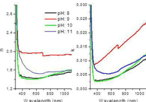
The refractive index is shown in Fig. 6. The refractive index and extinction coefficient of MnSe thin films were shown to be parallel with film thickness and the grain size at 1.42, 1.96, 1.39, 1.54 (refractive index) - 0.003, 0.012, 0.003, 0.005 (extinction coefficient) and were 117, 126, 84 and 79 nm (film thickness) and 4.63, 4.37, 5.78, 5.28 nm (grain size), respectively. Eid et al. also measured the refractive index of
Cd(1-x)MnxSe thin film at 600-2400 nm when x = 0.90 16-17.
They calculated the refractive index to be about 2.618 with 697 nm film thickness. The cadmium and film thickness affected the refractive index. Also, the film thickness in this study is
thinner than that reported in the literature.
The dielectric constant (ε) can be calculated by the following relation:
(9)
The dielectric constant changed with the refractive index at 0.131, 0.530, 0.116, 0.204 and at 1.42, 1.96, 1.39 and 1.54, respectively, as shown in Fig. 7. The dielectric
constant indicates the accessible electrical area. The
higher value of dielectric constant is pH: 9 as expected
because of the grains are oriented at a regular axis. The
electrical area affects the regular structure, because the
dipole moment vectors have the same orientation in the crystalline structure.
Figure 6. Plot of the refractive index and extinction coefficient of MnSe films at different pHs.
Figure 7. Plot of dielectric constant of MnSe films at different pHs.
Figure 8. SEM images of MnSe films at different pHs, (a) pH = 8, (b) pH = 9, (c) pH = 10, (d) pH = 11.
4. Conclusion
A new method was developed for producing MnSe thin films in this study. The production of MnSe thin films was scanned at different pHs of 11, 10, 9 and 8. The films had the best crystallinity at pH: 9. At pHs of 11 and 10 the MnSeO4 structure was observed. The grain size of the films
changed to at 4.63, 4.37, 5.78, and 5.28 nm depending
on the film thickness. These results very good than the literature. The film thicknesses of the films changed with the chemical bath pH’s at 79, 84, 126, 117 nm and pH: 11, 10, 9 and 8. These results agreed with the literature. The refractive index and extinction coefficient of the MnSe thin films were shown to be parallel with film thickness and the grain size at 1.42, 1.96, 1.39, 1.54 (refractive index) - 0.003, 0.012, 0.003, 0.005 (extinction coefficient), which were 117, 126, 84 and 79 nm (film thickness) and 4.63, 4.37, 5.78, 5.28 nm (grain size), respectively. These results agreed with the literature and the film thickness was thinner than the literature. Especially, the raw data’s (XRD) were used to in these studies.
5. References
1. Thanigaimani V, Angadi MA. Optical properties of MnSe thin
films. Thin Solid Films. 1994;245(1-2):146-151.
2. Wu M, Xiong Y, Jiang N, Niang M, Chen Q. Hydrothermal
preparation of α-MnSe and MnSe2 nanorods. Journal of Crystal
Growth. 2004;262(1-4):567-571.
3. Levy L, Feltin N, Ingert D, Pil MP. Three Dimensionally Diluted Magnetic Semiconductor Clusters Cd1-yMnyS with a Range of Sizes and Compositions: Dependence of Spectroscopic
Properties on the Synthesis Mode. Journal of Physical Chemistry
B. 1997;101(45):9153-9160.
4. Heimbrodt W, Goedea O, Tschentscher I, Weinhold V, Klimakow A, Pohl U, et al. Optical study of octahedrally and
tetrahedrally coordinated MnSe. Wide-Band-Gap Semiconductors.
1993;185:357-361.
5. Tomasini P, Haidouxv A, Tédenac JC, Maurin M.
Methylpentacarbonylmanganese as organometallic precursor
for the epitaxial growth of manganese selenide heterostructures.
Journal of Crystal Growth. 1998;193(4):572-576.
6. Murali KR, Trivedi DC. Characteristics of brush plated MnSe
films. In: 209th Electrochemical Society Meetings; 2006 May
7-12; Denver, CO, USA. p. 263.
7. Mahalingama T, Thanikaikarasan S, Dhanasekaran V, Kathalingam A, Velumani S, Rhee JK. Preparation and characterization
of MnSe thin films. Materials Science and Engineering: B.
2010;174(1-3):257-262.
8. Kariper IA, Baglayan Ö, Göde F. Fabrication and Optical Characterization of CdSe Thin Films, Grown by Chemical Bath
Deposition. Acta Physica Polinica A. 2015;128:B219-B221.
9. Kariper IA. Hardness of Mn2V2O7 thin films and its influential
factors. International Journal of Minerals, Metallurgy, and Materials. 2015;22(9):987-991.
10. Akaltun Y, Yildirim MA, Ates A, Yildirim M. The relationship between refractive index-energy gap and the film thickness effect on the characteristic parameters of CdSe thin films.
Optics Communications. 2012;284(9):2307-2311.
11. Yildirim MA, Ates A. Influence of films thickness and structure
on the photoresponse of ZnO films. Optics Communications.
12. Padiyan DP, Marikani A, Murali KR. Influence of thickness
and substrate temperature on electrical and photoelectrical
properties of vacuum deposited CdSe thin films. Materials
Chemistry and Physics. 2002;78(1):51-58.
13. Ates A, Yildirim MA, Kundakci M, Astam A. Annealing and light effect on optical and electrical properties of ZnS thin
films grown with the SILAR method. Materials Science in
Semiconductor Processing. 2007;10(6):281-286.
14. Shinde VR, Lokhande CD, Mane RS, Han SH. Hydrophobic and textured ZnO films deposited by chemical bath deposition:
annealing effect. Applied Surface Science. 2005;245(1-4):407-413.
15. Benramdane N, Murad WA, Misho RH, Ziane M, Kebbab Z. A chemical method for the preparation of thin films of CdO
and ZnO. Materials Chemistry and Physics.
1997;48(2):119-123.
16. Galyas AI, Demidenko OF, Makovetskii GI. Transmission
spectra of films of Mn1-xFex Se solid solutions. Journal of
Applied Spectroscopy. 2007;74(1):152-155.
17. Eid AH, Seddek MB, Salem AM, Dahy TM. Preparation and Characterization of Thermally Evaporated Cd Mn Se Thin
Films. Journal of Applied Sciences Research.