Article
Printed in Brazil - ©2018 Sociedade Brasileira de Química*e-mail: [email protected]
Electrochemical Deposition of the Single Phase Tl
xCu
3 – xSe
2Thin Films
Francisco W. S. Lucasa and Lucia H. Mascaro*,a
aDepartamento de Química, Universidade Federal de São Carlos, 13565-905 São Carlos-SP, Brazil
In spite of selenide semiconductors having a wide application area, TlCu2Se2 (TCSe) is poorly
studied and its synthesis by non-vacuum or thermic methodology in film form is non-existent. Generally, the main problems of applying these TCSe compounds are related to complicated single phase growth, and the great time consuming and non-scalable fabrication method. In this work, the facile, fast, scalable and new electrochemical deposition of this material was proposed as a workaround for these main problems and obtaining single phase thinfilm. Thus, the electrodeposited TlxCu3 – xSe2 films were characterized by scanning electron microscopy, X-ray diffraction (with
Rietveld refinement) and energy dispersive X-ray spectroscopy. They showed interesting variation of composition (x =1.1, 1.2, and 1.25) and morphology as function of the electrodeposition potential, electrolytic bath temperature and thermal treatment.
Keywords: Cu2TlSe2, thallium copper selenide, electrodeposition, texturization, chalcogenide
Introduction
Ternary chalcogenides semiconductors are potentially attractive electronic materials and have been applied in solid state semiconducting devices, gas sensor and in many other areas.1 In particular, copper thallium selenides are of
interest for the development of advanced thermoelectric
materials.2 The crystals of TlCu
2Se2 (TCSe) consist of
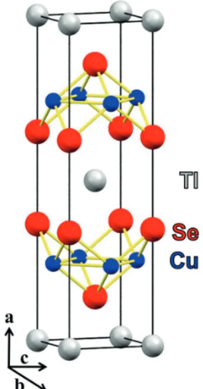
layered structures, where the Tl+ ions are located above and
below the layers.3,4 The unit cell can be seen in Figure 1.
It has been discussed that TCSe exhibits metallic properties and it possesses a relatively high conductivity (ρRT = 5 × 10⁻⁵ Ω cm).3,5 To account for this behavior,
Brun et al.5 believed the conductivity was caused by
the mixed-valence state of Tl+ and Tl3+ in the lattice.
However, it was demonstrated by Hall effect that this compound shows hole conductivity.3,6,7 This fact rules out
the existence of two oxidation state of thallium, because electrons would then fill the conduction band and act as charge carriers.3,6 Ohtani et al.7 investigated the electrical
nature of TlxCu3 – xSe2 (x = 1.1, 1.2 and 1.25) in more
detail, concluding that conduction occurs predominantly by holes, but there is also a small contribution of electrons. A substantial difference was not observed between the conductivities measured for pressed powders and for single crystals of TCSe, which is indicative of a weak anisotropy of the crystals resistance.3,6 Indeed, the electrical
and optical properties of group I-III-VI compound films are strongly related to the film growth techniques. TCSe has been prepared by heating, in sealed silica tubes in vacuum, stoichiometric amounts of TlSe, copper and selenium3,4 or elemental mixtures at 500 oC for 7 days. It
is then formed into a pellet, and annealed at 250 oC for
Figure 1. Unit cell of TlCu2Se2. For interpretation of the color references
7 days, followed by slow cooling.7 Moreover, as far as the
authors know, the synthesis of TCSe film by non-vacuum or thermic methodology is non-existent. In addition to this, TCSe is poorly studied. Thus, we propose TCSe thin film preparation by electrodeposition, which is a facile, fast and new fabrication methodology for this compound.
Experimental
Chemicals and apparatus
The chemicals (analytical grade) were used directly without further purification. The following reagents were used: CuSO4 (> 99.9%), Tl2SO4 (99.9995%), SeO2
(99.9%), and H2SO4 (98%). Electrochemical experiments
were performed in a potentiostat/galvanostat (PGSTAT 302N-Autolab, Metrohm-Eco Chemie). A three-electrode configuration electrochemical cell was used with a Mo or Pt plate (99.99%) as working electrode, a Pt plate as auxiliary
and an Ag/AgCl/Cl–
(sat. KCl) as reference electrode. The
composition and morphology of the films were evaluated by high-resolution field emission scanning electron microscopy (SEM; Zeiss Supra 35 FE-SEM) and energy dispersive X-ray (EDX) spectroscopy (FEI-XL30-FEG with an Oxford Instruments-Link ISIS 300 detector), respectively. The crystallographic films characterization was performed with the aid of an X-ray diffractometer
(XRD; Rigaku, DMax2500PC) with CuKα radiation,
counting time of 6 s and scanning step of 0.02o. The size
of the crystallographic coherence dominium (D, in nm) was estimated from the (103) TCSe peak by the Scherer equation and the line broadening (instrumental effects) was corrected with silicon powder standard (99%, 325 mesh, SRM-640) using the Caglioti equation, as described by Gonçalves et al.8 All samples were refined by the Rietveld
method9 through the General Structure Analysis System
(GSAS) program.10 The data available in the Inorganic
Crystal Structure Database (ICSD)11 were used as input
for the theoretical model.
TCSe films deposition
Cyclic voltammetry (CV) was used to evaluate the electrochemical process of the elements and its mixture on Pt. The CVs were recorded at a scan rate of 50 mV s-1, from
1.35 V vs. Ag/AgCl/Cl–
(sat. KCl) toward cathodic direction
and, for deaeration, a stream of N2(g) was introduced into
each solution for 10 min before each scan. Two potentials for electrodeposition of the TCSe films were chosen from these studies. Then, at a previously chosen more negative potential, different films were electrodeposited
using various electrolytic baths (EB) (with different ion concentrations) and analyzed by EDX. Thus, it was possible to choose the EB that formed films with composition close to the TlCu2Se2 phase. The temperature effect in film growth
was studied at 25 and 50 oC, performing electrodeposition
on Mo plate, using the optimized EB at each bath temperature and with total charge of 1 C (which resulted in ca. 1 h of deposition). Right before the electrodeposition,
Mo substrate (1 cm2) was cleaned ultrasonically with
acetone, ethanol and H2O/NH4OH (1:1) during 10 min, in
each solvent, then rinsed with deionized water and dried in an N2(g) stream. Thus, a 22 factorial design was performed
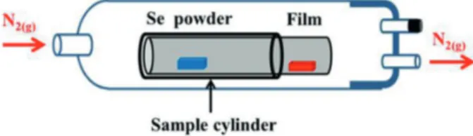
with two liberty levels for electrodeposition potential and EB temperature. In an attempt to observe the effect of the annealing, a film obtained in one of the experimental levels was annealed during 1 h in Se atmosphere and different
temperatures (150, 250 and 350 oC), with a heating/
cooling rate of 5 oC min-1. The film was placed into a lead
borosilicate glass cylinder (sample cylinder, volume of 300 mL) and the partial pressure of the Se(g) was controlled
by means of a crucible with 0.2 g selenium powder placed into this cylinder, which was not totally gas-tight (Figure 2). For this thermal treatment, a tube furnace was used and the atmosphere outside the sample cylinder was maintained at 1 atm of N2(g) and this gas exited the tube furnace through
a bubbler filled with mineral oil with flow of 1 mL min-1.
Results and Discussion
Electrochemical behavior
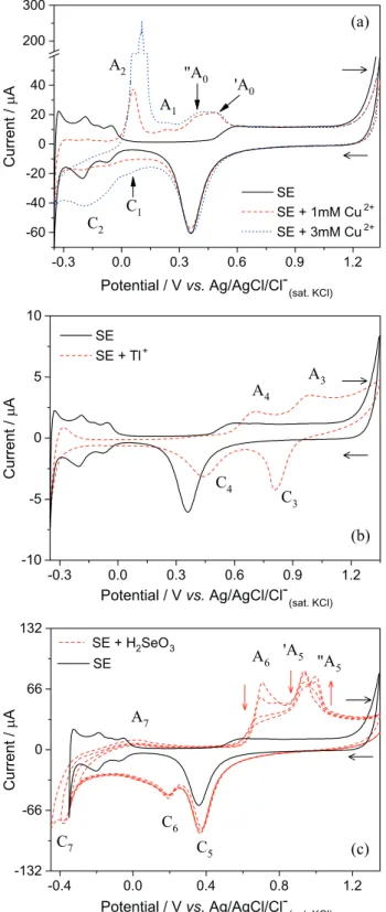
The electrochemical behavior of Pt electrode in 1 and 3 mmol L-1 of Cu2+, 8 mmol L-1 Tl+, and 1 mmol L-1
of H2SeO3 with supporting electrolyte (SE), 0.5 mol L-1
Na2SO4/H2SO4 and pH 2, was separately studied and the
voltammograms are presented in Figure 3.
In Figure 3a, the voltammograms for solutions containing
1 mmol L-1 (red dashed curve) and 3 mmol L-1 CuSO
4 (blue
dotted curve), and for blank solution (only SE; black solid curve) can be observed. A well-known electrochemical behavior of the Pt substrate in 0.5 mol L-1 Na
2SO4/H2SO4
and pH 2 (SE) was seen with peaks corresponding to hydrogen adsorption and desorption (0.0 to –0.3 V), and to
the formation (> 0.5 V) and reduction (ca. 0.4 V) of PtOx.
In the presence of Cu2+, two cathodic peaks (C
1 and C2) and
four anodic peaks ('A0, "A0, A1 and A2) appeared, and the
peaks corresponding to hydrogen adsorption/desorption were
inhibited due to the Cu underpotential deposition (UPD) that occurs between 0.05 and 0.005 V (C1), and the Cu bulk
deposition attributed to C2 peak. The anodic peaks can be
attributed to the redissolution of Cu-bulk phases (peak A2)
and Cu-adatoms layers (peaks 'A0, "A0 and A1). This behavior
is largely known in the literature.12-14
In Figure 3b, we can clearly observe the redox pair C3/A3 (at ca. 0.81/ca. 0.98 V, respectively) which can be
correlated to reduction/oxidation of the couple Tl3+/Tl+. In
the studies of Shin et al.15 on gold electrode, they observed
the reduction/oxidation potentials for this couple in the same potential window as this work on Pt. Moreover, they observed two peaks for UPD of Tl on Au-(111) at –0.255 and –0.365 V. Herein, we attributed the peaks
C4/A4 (at ca. 0.44/0.71 V) to Tl UPD on polycrystalline
Pt electrode. The inhibition of the hydrogen adsorption/ desorption reaction agrees with this attribution; Tl-adatoms are blocking the Pt electrochemical sites. Figure 3c shows the voltammograms for Se species with different inversion
potentials (Einv of –0.30, –0.35, –0.40 and –0.45 V). The
selenium electrochemical behavior is well-known;16-22 the
C5 (at ca. 0.37 V), C6 (at ca. 0.19 V) and C7 (at ca. –0.37 V)
processes can be assigned to UPD, massive (bulk) deposition (equation 1) and to Se0 (or H
2SeO3) reduction to
H2Se(aq/g) (equation 2), respectively. In the reverse scan, the
broad anodic peak A7 (around 0.01 V) may be associated
with oxidation of the H2Se(aq/g) or H2(g) adsorbed at the
electrode surface. The peak A6 (ca. 0.71 V) is assigned
to the dissolution of Se-bulk, and the 'A5 (at ca. 0.94 V)
and "A5 (at ca. 1.00 V) peaks are for the dissolution of the
first (Se on Pt) and last (Se on Se-adatom/Pt) Se layers, respectively. The dissolution peak area of the Se-bulk and last Se-adatoms layers decrease as long as the Einv become
more negative (from –0.30 to –0.45 V), because these layers are also dissolved when Se is reduced to H2Se. The increase
in "A5 peak area for more negative Einv may be evidence of
a better organization of the Se-adatoms layer, which allows the use of all available Pt sites and increases the number of Se-adatoms in this layer.
(1)
(2)
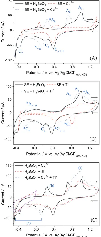
After that, the metals Cu2+ (Figure 4A) and Tl+
(Figure 4B) were studied in the presence of H2SeO3 and
then, the electrochemical profiles of all species together in solution (Figure 4C). Figure 4 shows the electrochemical behavior for the binary and ternary systems.
Comparing the individual electrochemical behavior of the species (shown in Figure 3) with the voltammogram of
Figure 3. Roomtemperature cyclic voltammograms on Pt and at scan rate of 50 mV s-1 for solutions: (a) 1 and 3 mmol L-1 CuSO
4; (b) 4 mmol L-1
Tl2SO4; and (c) 1 mmol L-1 H2SeO3 in 0.5 M Na2SO4/H2SO4 and
the binary systems, we can identify the peaks associated with the formation of binary phases or the presence of
a synergetic effect between the species. For example, in Figure 4A, it can be seen that the Cu presence increases the Se-bulk deposition or reduces its dissolution to H2Se,
which makes the A6 peak area increase, compared to the
individual behavior. The peak assigned as C5 + 0 means that
this peak can be a mixture of the individual processes C5
and C0. In turn, the new peaks *C8/*A8 can be associated
with the deposition/dissolution of the CuxSe (x = 2 is most
likely) phases (equation 3), as also described by other investigators.16,23
The voltammograms in Figure 4B show the electrochemical behavior for the Tl–Se binary system. The peaks *C3/*A3 are dislocated from the original potentials
observed in the absence of Se, caused, perhaps, by Tl−Se
layers adsorbed on Pt surface that add an additional resistance to the electrode. Comparing the voltammograms in the *C4 + 5 region, we can see that the Tl-adatoms layer
supress the Se-adatoms layer deposition, decreasing the
peak area associated with C5; however, the Se massive
deposition does not seem to be affected by Tl+ nor
Tl-adatoms presence. In addition, a new peak was observed
at about –0.2 V (*C9) with oxidation peak merged with the
C7 peak (*A7 + 9); these new processes can be attributed to
the Tl2Se deposition/dissolution (equation 5).
For the ternary system in Figure 4C, no new peaks were observed, but some of the voltammogram regions changed in relation to the binary systems. For clarity, the regions where noticeable changes were noted, letters from a to c were assigned. For example, the biggest change was viewed at region a; this variation could be resulted from the dissolution of the Cu–Tl–Se phase formed in forward scan, which takes place together with Se layers dissolution. The variation of the Cu–Se dissolution profile at region b can be associated with the small Tl incorporation into this phase. In turn, at region c, the peaks associated with the Tl–Se phase deposition
(*C9) and the H2Se formation (C7) were not observed.
The increase in the current that starts at the Cu–Se phase deposition potential (*C8), compared to the binary systems,
is an indication that the Cu–Tl–Se phase is being formed. The growth of this phase may happen in three ways: by Tl incorporation into Cu–Se and Se phases at potentials more negative than *C8 (equation 4); by the reaction between Se,
Cu–Se and Tl–Se, for potentials lower than *C9 (equation
6); and/or by the precipitation of Cu+/2+ and Tl+ with H 2Se
(formed according to equation 2), for potentials below
C7 (equation 7). These three electrochemical/chemical
mechanisms of deposition can be seen below:
(3)
(4)
Figure 4. Roomtemperature cyclic voltammograms on Pt and at scan rate of 50 mV s-1 for the binary systems (A) 1 mmol L-1 CuSO
4 +
1 mmol L-1 H
2SeO3 and (B) 4 mmol L-1 Tl2SO4 + 1 mmol L-1 H2SeO3;
and for the ternary system (C) 1 mmol L-1 CuSO
4 + 4 mmol L-1 Tl2SO4 +
1 mmol L-1 H
2SeO3 in 0.5 mol L-1 Na2SO4/H2SO4 at pH 2 (the first cyclic
(5)
(6)
(7)
From the electrochemical behavior seen in Figures 3 and 4 and based on the proposed mechanisms, the potentials chosen for TCSe films electrodeposition
were: –0.2 V (TlCu2Se2 deposition by mechanisms 4
and 6) and –0.4 V vs. Ag/AgCl/Cl–(sat. KCl) (TlCu2Se2
deposition predominantly by mechanism 7). It is worth mentioning that the platinum electrode was chosen for such electrochemical behavior studies because of its well-known behavior and electrochemical/chemical stability. In the case of molybdenum (the substrate chosen for films deposition), its open circuit potential in this SE is around 0 V vs. Ag/AgCl/Cl–
(sat. KCl), which makes it impossible to
study higher potential values, where this metal would be oxidized/dissolved. In contrast, Pt electrode has a great adsorptive character, showing great number of UPD depositions, which is not expected for Mo. However, in our study, at the potential region chosen for Cu–Tu–Se deposition, the mechanisms are dominated by massive depositions, which are not hugely affected by Pt adsorptive character, compared with Mo. For comparison, Figure 4C shows the cyclic voltammogram on Mo for the first scan in EB at the potential window where the Mo electrode is electrochemically stable. As can be seen in this Figure, there is no potential shift of the C7 peak on Mo, compared
to the same study on Pt. This observation was expected and corroborates our previous comments, since this process is associated with a massive deposition. After the first scan (not shown), the peak disappears, following the same behavior observed for Pt electrode.
From a previous study of the elements concentration
in EB, the optimized constitution was: 1 mM CuSO4,
4 mM Tl2SO4, 1 mM SeO2 and 0.5 M Na2SO4/H2SO4 at
pH 2 (supporting electrolyte). After that, the films were characterized by XRD (with Rietveld refinement; RR), SEM and EDX.
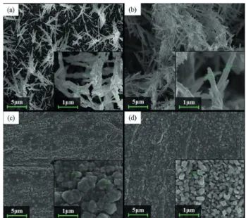
Films characterization
From 22 experiments, four different TCSe films were
obtained and their surface morphology was studied using SEM (Figure 5). The films electrodeposited at –0.4 V
and 25 or 50 oC were named as TCSe42 and TCSe45,
respectively. Likewise, the films electrodeposited at
–0.2 V and 25 or 50 oC were named as TCSe22 and
TCSe25, respectively.
The film electrodeposited at –0.4 V and 25 oC (Figure 5a)
showed a compact morphology with homogenously distributed structures like clusters of needles with medium diameter of about 70 nm. The increase of EB temperature
to 50 oC (Figure 5b) made the cluster grow and coalesce.
Comparatively, the films electrodeposited at –0.2 V (Figures 5c and 5d) had different morphologies, with smaller grains than those obtained at –0.4 V. The atomic composition of each film was evaluated by EDX and the contents are organized in Table 1. The estimate of the film thickness was based on the Faraday law with 100% efficiency and on its atomic composition; these data are also listed in Table 1.
The trend shown in Table 1 makes us conclude that the films composition was not significantly affected by the potential of deposition and bath temperature at the studied levels, with a standard deviation lower than 0.5% for triplicates. All deposited films showed Tl-rich/Cu-poor composition of the TlCu2Se2 phase; however, this change in
Tl/Cu ratio does not interfere in the charge balance of the TlCu2Se2 crystals, since the Se–Se lamellae have oxidation
state of –3 (–1.5 per Se atom) and both Tl and Cu atoms
have oxidation state of +1, as observed by Folmer and Jellinek.24
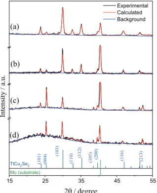
In order to prove and identify the phase formation, RR was performed on TCSe films diffraction patterns. In Figure 6, the experimental and calculated XRD patterns are shown. The tetragonal unit cell parameters, the size of the crystallographic coherence dominium (D) and RR parameters of the films are shown in Table 2.
A good match between the experimental and calculated
XRD patterns was observed, noted by the small Rwp value
(Table 2) and variation along the diffraction angle, as shown in Figure 6. Thus, by comparison with standard
non-texturized TlCu2Se2 (space group I 4/m m m, ICSD
code 629124) pattern available in the ICSD,11 it was proven
that all films were single phase TlCu2Se2. Also, some of
the peaks were attributed to Mo substrate (associated with the ICSD code 52267 standard, space group I m-3 m). Comparing the relative intensities of the peaks (004) and (103) with those from standard non-texturized TlCu2Se2, we
can conclude that the films electrodeposited at –0.4 V did not show texturing phenomenon. On the other hand, those electrodeposited at –0.2 V presented a notable increase in the number of domains with the TlCu2Se2 [004] crystalline
plane oriented parallel to the substrate surface, noticed by the increase in the (004) peak intensity relative to the (103) peak. This texturization can also be associated with the morphology seen in Figure 5d.
Based on D values organized in Table 2, it was interesting to observe that the increase in EB temperature noticeably improved the films crystallinity for films deposited at –0.4 V, while only a small improvement was observed for those deposited at –0.2 V. These aforementioned observations make us probe that TlCu2Se2 growth mechanism is different
for each deposition potential applied. For potentials more negative than –0.4 V vs. Ag/AgCl/Cl–(sat. KCl), the H2SeO3
Table 1. Approximate atomic composition of the films
Film Cu / atom% Tl / atom% Se / atom% Formula Thicknessa / µm
TCSe42 38 22 40 Cu1.9Tl1.1Se2 1.05 ± 0.53
TCSe45 35 25 40 Cu1.75Tl1.25Se2 1.08 ± 0.82
TCSe22 38 22 40 Cu1.9Tl1.1Se2 1.07 ± 0.25
TCSe25 36 24 40 Cu1.8Tl1.2Se2 1.07 ± 0.34
aEstimated from Faraday law with 100% efficiency, taking into account the composition and crystallographic parameters of each film listed in Table 2. The
standard deviation for all elements is lower than 0.5 atom%. TCSe42 and TCSe45: films electrodeposited at –0.4 V and 25 or 50 oC, respectively; TCSe22
and TCSe25: films electrodeposited at –0.2 V and 25 or 50 oC, respectively.
Table 2. Rietveld refinement (RR) and tetragonal unit cell parameters (for better visualization, see Figure 1) and the size of the crystallographic coherence dominium (D) of the TCSe films
Film RR parameter Cell parameter Da / nm
Rwp / % RBragg / % χ2 a = b / Å c / Å V / Å3
TCSe42 25.13 8.79 1.253 3.8698 13.9604 209.062 17.82
TCSe45 16.81 8.35 2.027 3.8828 14.0365 211.613 30.31
TCSe22 25.85 14.07 1.777 3.8858 14.0085 211.517 23.20
TCSe25 20.60 20.44 1.073 3.8816 13.9938 210.840 24.20
aEstimated from the (103) TCSe peak. RR: Rietveld refinement; R
wp: weighted-profile Rietveld factor; RBragg: reflection intensity-based Rietveld factor; χ2: chi-squared (related with the goodness of fit); a, b and c: lattice parameters; V: volume; D: crystallographic coherence dominium; TCSe42 and TCSe45: films electrodeposited at –0.4 V and 25 or 50 oC, respectively; TCSe22 and TCSe25: films electrodeposited at –0.2 V and 25 or 50 oC, respectively.
Figure 6. Experimental and calculated X-ray diffraction patterns of the films (a) TCSe42, (b) TCSe45, (c) TCSe22 and (d) TCSe25. Standard diffraction patterns for TlCu2Se2 (ICSD code 629124) and Mo (ICSD
(or Se0) species are electrochemically reduced to H 2Se.
This Se2– source can chemically react with the metals
(Tl and Cu) in solution, precipitating as non-texturized
TlCu2Se2 (insoluble salt) on the electrode surface. The
H2Se(g/aq) solubility/concentration is strongly affected by
the EB temperature, explaining the high effect of this parameter in the film crystallinity. In turn, the mechanism for electrochemical deposition at –0.2 V involves reaction in solid phase of elemental Se0 with the metal ions (or Cu
ySex
with Tl+ ions) to grow the TlCu
2Se2 compound. This last
growth phenomenon is less affected by temperature and more surface confined than the first one, which can explain the fact that the films electrodeposited at this potential are texturized and their crystallinity are less influenced by EB temperature. Other authors proposed similar mechanisms for the In–Cu–Se system.20-22
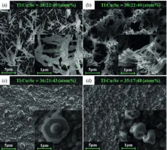
Finally, the less crystalline film, TCSe42, was chosen to study the annealing effect on the material crystallinity, crystallographic phase, composition and morphology.
Thus, this film was annealed at 150, 250 and 350 oC in
Se atmosphere during 1 h. The effect of this treatment on surface morphology and composition can be seen in Figure 7.
From Figure 7, we observe a marked change on film
surface with thermal treatment. The annealing at 150 oC
(Figure 7b) did not change the film composition, but caused the increase of the number of clusters of needles, as well as change in the needle shape. This behavior can be associated with sublimation and condensation of TlCu2Se2 in Se vapor
atmosphere during the annealing, which changed the needle shape and density. It is worth mentioning that the decrease
of film crystallinity after annealing in Se atmosphere was not expected, since the crystallinity of a great variety of selenide semiconductors has been improved after such
treatment.22,25 On other hand, from 150 to 250 oC, the
clusters melt and Tl begins to sublime, while the films
treated at 250 and 350 oC (Figures 7c and 7d) do not have
clusters and the Se content increases. To observe any phase transition during these thermal treatments, the films were characterized by XRD. The diffraction patterns as a function of annealing temperature can be seen in Figure 8.
As the diffraction peaks showed low intensity, close to noise level, it was not possible to perform the RR on diffraction patterns of the thermally treated films. However, it was possible to roughly estimate that the size of the crystallographic coherence dominium of the TCSe42
film annealed at 150 oC is almost half the as-deposited
one, despite the annealed film seeming to be single phase TlCu2Se2. Thus, we can conclude that the thermal treatment
at temperatures above 150 oC reduces the crystallinity of the
films. Additionally, the films annealed at 250 and 350 oC
were almost amorphous, making any phase identification difficult. Nevertheless, based on the composition, we believe that as long as Tl sublimes from the films they
become amorphous CuxSe.
Conclusions
The electrodeposition of a good quality single phase TlxCu3 – xSe2 with different compositions (x = 1.1, 1.2
and 1.25), morphology, crystallinity and crystallographic texturization was achieved. An interesting variation
Figure 7. SEM micrographs of the TCSe42 film (a) as-deposited; and annealed at (b) 150, (c) 250 and (d) 350 oC.
Figure 8. Experimental X-ray diffraction patterns of the TCSe42 films thermally treated at (a) 150, (b) 250 and (c) 350 oC. Standard diffraction
patterns for TlCu2Se2 (ICSD code 629124) and Mo (ICSD code 52267)
of morphology as a function of the electrodeposition potential, the electrolytic bath temperature and thermal treatment was observed. The films electrodeposited at
–0.2 V vs. Ag/AgCl(sat. KCl) were texturized with [004]
crystallographic planes parallel to substrate surface, which could be related to observed tetragonal morphology.
Generally, the main problems of applying these TCSe compounds are related to the complicated growth of a single phase, the great time consumed and non-scalable fabrication method. In this work, using a facile, fast, scalable and new methodology these main problems were solved and it was possible to obtain a single phase TlxCu3 – xSe2 (x = 1.1, 1.2 and 1.25)thinfilm.
Acknowledgments
This work was supported by the São Paulo Research Foundation (FAPESP) grants 2012/10947-2 and 2016/10513-3; and CEPID grant 2013/07296-2.
References
1. Makovicky, E.; Rev. Mineral. Geochem. 2006,61, 7.
2. Matsumoto, H.; Kurosaki, K.; Muta, H.; Yamanaka, S.;
J. Electron. Mater. 2009, 38, 1350.
3. Starodub, V. A.; Russ. Chem. Rev.1999,68, 801.
4. Klepp, K.; Boller, H.; Monatsh. Chem. 1978, 109, 1049. 5. Brun, G.; Gardes, B.; Tedenac, J. C.; Raymond, A.; Maurin,
M.; Mater. Res. Bull. 1979, 14, 743.
6. Berger, R.; Van Bruggen, C. F.; J. Less-Common Met. 1984, 99,
113.
7. Ohtani, T.; Taniguchi, M.; Sasaki, S.; Kishi, H.; Nakata, T.;
J. Alloys Compd. 2004, 383, 245.
8. Gonçalves, N. S.; Carvalho, J. A.; Lima, Z. M.; Sasaki, J. M.;
Mater. Lett.2012,72,36.
9. Young, R. A.; Rietveld Method; Oxford University Press:
London, 1995.
10. Larson, A. C.; Von Dreele, R. B.; General Structure Analysis System (GSAS); Los Alamos National Laboratory Report LAUR
86-748, 1994.
11. https://www.fiz-karlsruhe.de/de/leistungen/kristallographie/ icsd.html, accessed in June 2018.
12. Danilov, A. I.; Molodkina, E. B.; Polukarov, Y. M.; Climent, V.; Feliu, J. M.; Electrochim. Acta 2001, 46, 3137.
13. Molodkina, E. B.; Danilov, A. I.; Feliu, J. M.; Russ. J. Electrochem.2015, 56, 999.
14. Marković, N. M.; Grgur, B. N.; Lucas, C. A.; Ross, P.;
Electrochim. Acta1998, 44, 1009.
15. Shin, J. W.; Bertocci, U.; Stafford, G. R.; J. Phys. Chem. C 2010, 114, 17621.
16. Steponavičius, A.; Šimkūnaitė, D.; Russ. J. Electrochem.2002, 38, 488.
17. Santos, M. C.; Machado, S. A. S.; J. Electroanal. Chem.2004, 567, 203.
18. Kemell, M.; Saloniemi, H.; Ritala, M.; Leskelä, M.; Electrochim. Acta2000, 45, 3737.
19. Beni, V.; Collins, G.; Arrigan, D. W. M.; Anal. Chim. Acta2011, 699, 127.
20. Lucas, F. W. D. S.; Lima, A. R. F.; Mascaro, L. H.; Electrochim. Acta2014, 147, 47.
21. Lucas, F. W. S.; Mascaro, L. H.; ECS Trans.2013, 58, 355.
22. Lucas, F. W. D. S.; Lima, A. R. F.; Mascaro, L. H.; RSC Adv. 2015, 5, 18295.
23. Šimkūnaitė, D.; Ivaškevič, E.; Kaliničenko, A.; Steponavičius, A.; J. Solid State Electrochem. 2005, 10, 447.
24. Folmer, J. C.; Jellinek, F.; J. Less-Common Met.1980, 76, 153. 25. Costa, M. B.; de Souza Lucas, F. W.; Mascaro, L. H.;
ChemElectroChem2017, 4, 2507.
Submitted: January 15, 2018
Published online: June 25, 2018