Abstract —An approach to scattering parameter calculation for a wave digital model of elliptic structure is described. The z-domain scattering parameters are given via wave transfer parameters. The main purpose of this paper is to show that the resultant equations for a wave digital model of elliptic structure can be used in the analysis of the models of structures with open/short-circuited stubs. This possibility reduces the number of wave digital network types, and contributes to the generalization of applied analysis approach and its software implementation.
Keywords —Microstrip structure, wave digital networks, z -domain functions, scattering parameters, open and short-circuited stubs.
I. INTRODUCTION
HE wave digital filter theory introduced by A. Fettweis [1], [2] has proven to be a very powerful tool for modeling of planar microstrip structures by wave elements. Till now, the wave digital approach has been efficiently applied for the analysis of structures with different geometries in both time and frequency domains [3]-[14].
The key element of wave approach is the introduction of wave variables A and B, which allow response calculation in one-dimensional (1D) wave digital networks (WDNs). The WDNs depend on structure geometry. This reflects the richness of WDNs which correspond to: stepped-impedance structures [6]-[8], stub-line structures [9]-[12], as well as elliptic structures with series connected transmission lines in parallel branches [14], [15].
In Section II, this paper outlines the concept of WDN and its use for the modeling and analysis of microstrip circuits. Moreover, special emphasis has been put on a plain but concise presentation of the underlying ideas in order to address both readers with and without background in wave digital approach.
A goal of this paper is to present an application way of the resultant equations for elliptic structure digital model [15] to models of structures with open/short-circuited stubs, what is explained in Section III. This is a great opportunity to use the same WDN for modeling of different planar structures with similarity in their
This paper is supported by the Ministry of Science and Technological Development of Serbia, project number TR32052.
Biljana P. Stošić is with the University of Niš, Faculty of Electronic Engineering, Aleksandra Medvedeva 14, 18000 Niš, Serbia (phone: 381-18-529303; e mail: [email protected]).
geometry. This reflects to reducing of total WDN types, and software implementation of a given approach in MATLAB environment becomes simplified.
To prove the accuracy of the proposed approach, in Section IV, the computer simulated results of WDNs are compared to those obtained in known software.
II. A BRIEF REVIEW OF WAVE DIGITAL APPROACH In this paper, the author will mainly be dealing with a 1D wave digital approach. Some general properties and the basic aspects of this approach that are of considerable importance, related to this work, will be discussed here briefly. Generally speaking, the block-based 1D wave digital approach to analysis entails modeling structure as a network of interconnected blocks.
A complex structure has to be divided into a cascade connection of uniform transmission lines (so-called uniform segments, assigned as UTL segments in figures) where each segment is modeled by unit wave digital elements. A lossless uniform transmission line is modeled by a two-port digital element with a delay occurring in the forward path. This wave digital two-port network is called the unit element (UE) [2]. Each UE is associated with its delay and port resistances. The port resistances of the UE are equal and correspond to the characteristic impedance of uniform segment. The connection of two UE with different port resistances is achieved by two-port series/parallel adaptors [3].
In the complex microstrip structures, the delays of transmission lines vary from one another, and because of this each uniform segment (transmission lines) has to be represented as a cascade connection of a certain number of UEs. A way of determining minimal section numbers (i.e. UEs) in WDN is based on the given relative error as shown below. An appropriate choice of a minimal section number in that model is very important because of the direct influence on the sampling frequency of that digital model, and on accuracy of the desired response.
A. Minimal Section Numbers [7]
A real delay TΣ of a complex microstrip structure
differs from the delay Tt of the WDN. In complex microstrip structures, delays of transmission lines are not multiple integers of the minimum delay. The number of sections nk used for modeling an individual transmission line is found as the nearest integer of the ratio q⋅Tk Tmin
Application of the Equations for Elliptic
Structure Digital Model to Models of Structures
utilizing Open/Short-circuited Stubs
Biljana P. Stošić, Member, IEEE
[
min]
roundq T Tnk = ⋅ k , (1)
where q≥1 is a multiple factor, Tk is a delay on the kth transmission line, Tmin =min
{
T1,T2,...,TM}
is a minimum delay, k=1,2,...,M and M is the number of uniform segments in the complex microstrip structure.According to these data, the total delay for the digital model of the structure is
q T n
Tt = t⋅ min , (2)
where the total number of UE in the WDN is
∑
== M
i k
t n
n 1 . (3)
The relative error of a total delay in percentages is found as
[ ]
% = − ⋅100Σ Σ
T T T
er t , (4)
where
∑
=Σ=
M k Tk T
1 (5)
is the sum of all transmission line delays, i.e. the total real delay of the structure, and Tt is given by (2).
The minimal number of sections needed for the modeling of the observed structure is found by using the relative error n_er
[ ]
% , which is already known. The procedure for determining the minimal number of sections with the error less than the given one can be done in a few steps. At the beginning, errors er[%] are found for different values of the multiple factor q=1,2,...,qmax, where qmax is an arbitrary chosen value. Then, the first relative error with an absolute value less than the previously given error er[ ]
% ≤n_er[ ]
% is chosen. The number of sections for the kth transmission line nk,M
k=1,2,..., , the total number of sections nt, and the total delay of a digital model of the structure Tt, corresponding to that error are then used for modeling.
B. Sampling Frequency
The sampling frequency of the digital model of the planar structure is found for the chosen minimal number of sections, and is
s
s T
F =1/ , (6)
where
t t s T n
T = / (7)
is the sampling period of the planar structure modeled by t
n sections. In order to match the response of the digital model with a real response, a new frequency is defined
2 / s sm F
F = . (8)
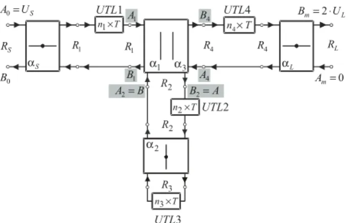
III. WAVE DIGITAL NETWORK PARAMETERS Given is a wave digital network of an elliptic structure (structure with series connected transmission lines in parallel branch), Fig. 1. A WDN can be generally seen as a set of uniform segment models (assigned as nk×T blocks) connected with each other through a tree-like network of elementary (series or parallel) adaptors.
Furthermore, to any port can be assigned a port resistance Rk, by choosing for Rk any arbitrary constant including 0 and ∞. Although in practice one will select that particular value of Rk which leads to the simplest overall expressions for the problem at hand.
Fig. 1 illustrates a resultant network, i.e. structure model, that consists of =
∑
4=1 k k
t n
n UEs, one three-port parallel adaptor, and three two-port series adaptors. The incident wave A0 is equal to voltage US of the source, and reflected wave Bm is equal to voltage 2⋅UL on the load. The first and the last two-port series adaptors are used for matching source and load resistances to the rest of the WDN.
1
α
2
R UTL1
T
n1× n T
4× UTL4
UTL2 T n2×
3
α
T n3×
UTL3 2
R
3
R
2
α 1 A
1 B
S
R R1 R1 R4 R4 RL
L
m U
B =2⋅
0 =
m
A
S
α αL
S
U A0=
0 B
4 B
4 A B
A2= B2=A
Fig. 1. WDN of an elliptic structure.
Response in WDN can be calculated in the frequency or in the time domain directly from known network function in z-domain. The network function is obtained by use of wave matrices S and T. An approach for direct counting of polynomial coefficients of rational functions S21 and
11
S is described here.
The network scattering parameters in z-domain can be given via wave transfer parameter formulation [4]. A network can be viewed as a combination of multiport subnetworks. So, the solution can be summarized as follows: 1. find wave transfer matrices T of subnetworks (one- and two-port subnetworks), 2. multiply all T matrices to get the overall T matrix, and 3. convert the T matrix into S matrix. This procedure is given below.
A. The Wave Transfer Matrices of Subnetworks
The wave transfer matrix of kth two-port series adaptor is
⎥ ⎦ ⎤ ⎢
⎣ ⎡ −
− ⋅
− =
1 1 1 1
k k
k
k α
α α
α
T , (9)
where the adaptor’s coefficient is
1 1
+ +
+ − =
k k
k k k
R R
R R
α , k=0,2,4, (10)
and R0 =RS, and R5 =RL are the port resistances of source and load, respectively. The other resistances are port resistances of UEs. For the coefficients it can be written α =0 αS and α =4 αL.
⎥ ⎥ ⎦ ⎤ ⎢ ⎢ ⎣ ⎡ ⋅ = − − 1 0 0 1 1 1 z z UE
T , (11)
and for one uniform segment which is modeled by nk cascaded UEs is
⎥ ⎥ ⎦ ⎤ ⎢ ⎢ ⎣ ⎡ ⋅ = × × × = − − 1 0 0 1 k k k k n n n UE UE UE n UE z z 4 4 4 3 4 4 4 2
1 T L T
T
T . (12)
Consider now a part of WDN from Fig. 1, i.e. one-port network shown in Fig. 2 which represents a digital model of series connected two transmission lines, where the second one is an open stub. The proof is given in [14]. A uniform segment UTL2 is modeled with n2 cascaded UEs, and segment UTL3 with n3 UEs. Connection between these two models of uniform segments UTL2 and UTL3 is achieved by a two-port series adaptor with coefficient α2
given by (2), symbolically represented in Fig. 2. 2
UTL
T n2×
2
α
T n3×
3
UTL
2
R R3
2 R 2 A 2 B A B 1 A 1 B
Fig. 2. WDN of series connected two transmission lines. Observed is a case where port resistances differ from one another R2 ≠R3, as well as section numbers n2≠n3. It means that a series connection of a transmission line and an open stub with different characteristic impedances and UE numbers is described. The relations for the left network part are
A z A = −n2⋅
1 , (13)
1 B
B= . (14)
Starting from the equations for a two-port series adaptor ), ( ), ( 2 1 2 1 2 2 1 2 2 1 A A A B A A A B + ⋅ + − = + ⋅ − − = α α (15) and by using equations (13) and (14), and the relation for
wave variables of stub assigned as UTL3 2 2 z 3 B
A = −n ⋅ , (16)
the relation between the main wave variables of network is found as
A z z z B n n n ⋅ ⋅ − − ⋅ = − − − 3 3 2 2 2 1 ) ( α α . (17) Now, a wave transfer matrix of three-port parallel
adaptor with WDN of Fig. 2 on its dependent port, has to be found. Consider the central part of Fig. 1. The equations of three-port parallel adaptor with port 2 being dependent are
1 2 2
1 B A A
B = + − ,
4 2 2
4 B A A
B = + − , (18)
) ( )
( 1 2 3 4 2
1 2
2 A A A A A
B = +α − +α − ,
where the adaptors’ coefficients depend on port conductances as 4 2 1 1 1 2 G G G G + + ⋅ =
α and
4 2 1 4 3 2 G G G G + + ⋅ =
α . (19)
Finally, the wave transfer matrix of this observed two-port subnetwork is found from relations (17)-(18) after some substitutions in (18) like B2= A and A2=B, and has a form
⎥ ⎦ ⎤ ⎢ ⎣ ⎡ ⋅ = ) ( ) ( ) ( ) ( ) ( 1 22 21 12 11 ,3 2 3
1 Q z Q z
z Q z Q z W n n α α
Τ . (20)
The wave matrix elements are the rational polynomial functions of z−1. The polynomials of matrix elements are
) ( 2
2
11( ) 2 3 2 3
n n n n z z z z
Q =−α−α ⋅ − +α⋅α ⋅ − + − + , (21)
, ) 1 ( ) 1 ( ) 1 ( 1 ) ( ) ( 3 1 2 3 2 1 12 3 2 3 2 n n n n z z z z Q + − − − ⋅ − + ⋅ − ⋅ + + ⋅ − ⋅ + − = α α α α α α (22) , ) 1 ( ) 1 ( ) 1 ( 1 ) ( ) ( 1 3 2 1 2 3 21 3 2 3 2 n n n n z z z z Q + − − − ⋅ − + ⋅ − ⋅ + + ⋅ − ⋅ + − = α α α α α α (23) ) ( 2 2
22( ) 1 2 3 2 3
n n n n z z z z
Q = +α⋅α ⋅ − −α ⋅ − −α⋅ − + , (24) ) 1
( )
(z 1 2 z n2 2 z n3 z (n2 n3)
W =α ⋅ −α ⋅ − −α ⋅ − + − + (25) and
3 1
1 α α
α = − − . (26)
The coefficients’ order in these polynomials is for the case of n2 <n3.
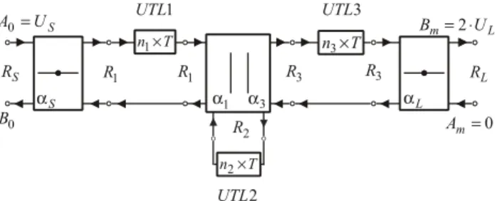
B. The Wave Transfer Matrix Modified for the Network of Structure Utillizing an Open Stub
Now, a suitably chosen port resistance R3→∞ is assigned to one of the ports in Fig. 2. In this case, the network corresponds to an open stub UTL2. The adaptor’s coefficient according to equation (10) is
1 2=−
α . (27)
By replacing (27) in the first relation of equation (15), the relation between the wave variables in Fig. 2 is obtained
1 1 B
A = . That implies further A z
B= −n2⋅ . (28)
Starting with relations (21)-(25) and (27), with assumption of z−n3 =0 (block n ×T
3 has no elements), the element polynomials of wave transfer matrix 2 3
3 1 ,n n α α
Τ for a three-port adaptor with a model of open stub on dependent three-port, are found as
2
) (
11 z z n
Q =−α+ − , (29)
2 ) 1 ( 1 )
( 1 3
12
n z z
Q =α − + −α ⋅ − , (30)
2 ) 1 ( 1 )
( 3 1
21
n z z
Q = −α + α − ⋅ − , (31)
2 1 ) ( 22 n z z
Q = −α⋅ − (32)
and ) 1 ( ) ( 2 1 n z z
W =α ⋅ + − . (33)
The polynomials of 2 3 1
n
α α
0
B S U A0=
1
R R3
S R
L
m U
B =2⋅
3
R RL
0
= m A L α 1
α S
α
1
R
3 α
2
R
1
UTL
2
UTL T n2×
T
n1× n3×T
3
UTL
Fig. 3. WDN of the structure given in Fig. 1 modified for the case of open stubs.
C. The Wave Transfer Matrix Modified for the Network of Structure Utillizing a Short-circuited Stub
If the port resistance has value R3 =0 (Fig. 2), then the network corresponds to a short-circuited stub UTL2. In that case, the adaptor’s coefficient according to equation (10) is
1 2 =
α . (34)
By replacing (34) in the first relation of equation (15), the relation between the wave variables in Fig. 2 is obtained
1 1 B
A = . That implies further A z
B=− −n2⋅ . (35)
Starting with relations (21)-(25) and (34), with assumption of z−n3 =0 (block n ×T
3 has no elements), the element polynomials of wave transfer matrix 2 3
3 1
,n n
α α
Τ for adaptor with a model of short-circuited stub on dependent port, are found as
2
) ( 11
n z z
Q =−α− − , (36)
2
) 1 ( 1 )
( 1 3
12
n z z
Q =α − + α − ⋅ − , (37)
2
) 1 ( 1 )
( 3 1
21
n z z
Q = −α + −α ⋅ − , (38)
2
1 ) ( 22
n z z
Q = +α⋅ − (39)
and
) 1 ( )
( 2
1
n z z
W =α ⋅ − − . (40)
WDN from Fig. 1, modified for a case of structure with a short-circuited stub, is depicted in Fig. 4.
0
B S U A0=
1
R R3
S R
L
m U
B =2⋅
3
R RL
0
= m A L α 1
α S
α 1
R
3 α
2
R
1
UTL
2
UTL T n2×
T
n1× n3×T
3
UTL
1 −
Fig. 4. WDN of the structure given in Fig. 1 modified for the case of short-circuited stubs.
D. The Overall Wave Transfer Matrix
The overall wave transfer matrix T of resultant analyzed network is a product of the wave matrices of network building blocks, i.e. subnetworks
L S
n UE n n n
UE αα α
α T T T T
T
T = × × 2 3× 4×
3 1
1 , . (41)
The equation system of network shown in Fig. 1 is m
m T B
A T
B0 = 11⋅ + 12⋅ , (42)
m
m T B
A T
A0= 21⋅ + 22⋅ , (43)
where the overall wave transfer matrix can be written in the form of polynomials
⎥ ⎦ ⎤ ⎢
⎣ ⎡ ⋅ = ⎥ ⎦ ⎤ ⎢
⎣ ⎡ =
) ( ) (
) ( ) ( ) ( 1 ) ( ) (
) ( ) (
22 21
12 11
22 21
12 11
z F z F
z F z F z R z T z T
z T z T
T . (44)
The wave matrix elements are the rational polynomial functions of z−1. Generally, the network functions are found as
• reflection coefficient
) (
) ( ) (
) (
22 12 22
12
0 0 0 11 0
z F
z F z T
z T A
B S
m
A
= =
= = Γ
=
, (45)
• transmission coefficient
) (
) ( ) ( 1
22 22
0 0 21
z F
z R z T A
B S
m
A
m = =
=
=
. (46)
IV. SIMULATION RESULTS
To prove approach accuracy, the equations derived for network with two series connected transmission lines and corresponding approximations given above are applied for response calculation in two examples. The third uniform segment UTL3 does not exist then. Some theoretical models given in [6]-[12] and [16] are used for discontinuity characterization.
A. Structure Utilizing an Open Stub
Given is a structure utilizing an open stub UTL2, Fig. 5. The substrate material has a relative dielectric constant
32 . 2
=
r
ε and a high h=1.58mm. Segment parameters are given in Tables 1 and 2.
UTL2
UTL1 UTL4
Input Output
1 d
2 d
4 d
1 w
2 w
4 w
Fig. 5. Layout of T-resonator.
TABLE 1: SEGMENT PARAMETERS WITHOUT MODELED DISC.
nv d [mm] w [mm] Zc [Ω] Tv [ps]
1 30.0000 4.7100 50.2540 139.8003 2 30.0000 15.7600 20.0016 145.0746
3 0.0000 0.0000 0.0000 0.0000
4 30.0000 4.7100 50.2540 139.8003
TABLE 2: SEGMENT PARAMETERS WITH MODELED DISCONTINUITIES.
nv d [mm] w [mm] Zc [Ω] Tv [ps]
1 22.1200 4.7100 50.2540 103.0794 2 28.4681 15.7600 20.0016 137.6665
3 0.0000 0.0000 0.0000 0.0000
For the case of given error of 0.01%, q=134 is a multiple factor and a total minimal number of sections in WDNis nt =447. The numbers of sections in individual segments are 134, 179, 0, and 134, respectively. The analysis parameters are: a total delay for the digital model of the structure is Tt =343.8254ps for a minimum delay
{
, ,}
103.0794psmin 1 2 4
min = T T T =
T . A real delay of the
structure is TΣ=343.8544ps. A sampling frequency of the digital model of the planar structure is
GHz 9687 . 1299
=
s
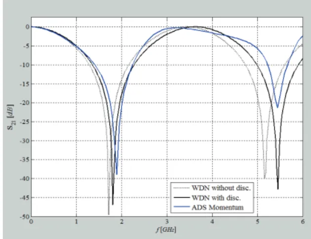
F . In this case, a relative error of delay is er=−0.008457%. The three-port adaptor coefficients are α1=α3=0.4432. The two-port adaptor coefficients are α2=−1, and αS =−αL=−0.0025. Frequency responses are depicted in Figs. 6 and 7.
Fig. 6. Frequency response S21.
Fig. 7. Frequency response S22.
The transmission S21 and reflection S11 coefficients, equations (46) and (45), have polynomials in numerator
179 4432 . 0 4432 . 0 )
(z = + ⋅z−
R ,
, 0025 . 0 5568
. 0 0003
. 0
0003 . 0 5568
. 0 0025 . 0 ) (
447 313
268
179 134
12
− −
−
− −
⋅ − ⋅ + ⋅ +
+ ⋅ − ⋅ − =
z z
z
z z
z F
and polynomial in denominator
. 10 4180 . 6 0028
. 0 10
2890 . 7
1136 . 0 0028 . 0 1 ) (
447 6 313
268 7
179 134
22
− − −
− −
− −
⋅ ⋅ − ⋅ + ⋅ ⋅ +
+ ⋅ − ⋅ − =
z z
z
z z
z F
B. A Structure Utilizing a Short-circuited Stub
Given is a structure utilizing a short-circuited stub UTL2, Fig. 8. The substrate material has a relative dielectric constant εr =4.6 and a high h=0.6mm. Metallization is t=17.5μm thick. Segment parameters are given in Tables 3 and 4.
UTL2
UTL1 UTL4
Input 1 Output
d
2
d
4
d
1
w
2
w
4
w
Fig. 8. Layout of a microstrip structure utilizing short-circuited stub.
TABLE 3: SEGMENT PARAMETERS WITHOUT MODELED DISC.
nv d [mm] w [mm] Zc [Ω] Tv [ps]
1 3.1000 1.1000 48.9868 19.4386 2 18.0000 1.5000 40.4218 114.6903
3 0.0000 0.0000 0.0000 0.0000
4 3.1000 1.1000 48.9868 19.4386
TABLE 4: SEGMENT PARAMETERS WITH MODELED DISCONTINUITIES.
nv d [mm] w [mm] Zc [Ω] Tv [ps]
1 2.3500 1.1000 48.9868 14.7357 2 17.4500 1.5000 40.4218 111.1858
3 0.0000 0.0000 0.0000 0.0000
4 2.3500 1.1000 48.9868 14.7357 For the case of given error of 0.01%, q=11 is a multiple factor and a total minimal number of sections in WDN is nt=105. The numbers of sections in individual segments are 11, 83, 0, and 11, respectively. The analysis parameters are: a total delay for the digital model of the structure is Tt =140.6572ps for a minimum delay
{
, ,}
14.7357ps min 1 2 4min = T T T =
T . A real delay of the
structure is TΣ=140.6590ps. A sampling frequency of the digital model of the planar structure is
GHz 4863 . 746
=
s
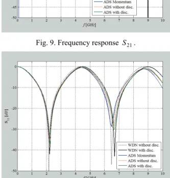
F . In this case, a relative error of delay is er=−0.001234%. The three-port adaptor coefficients are α1=α3=0.6227. The two-port adaptor coefficients are α2=1, and αS =−αL=0.0102. Frequency responses are depicted in Figs. 9 and 10.
The transmission S21 and reflection S11 coefficients, equations (46) and (45), have polynomials in numerator
83 6226 . 0 6226 . 0 )
(z = − ⋅z−
R ,
, 01024 . 0 3774
. 0 002512
. 0
002512 . 0 3774
. 0 01024 . 0 ) (
105 94
83
22 11
12
− −
−
− −
⋅ −
⋅ − ⋅ +
+ ⋅ +
⋅ − −
=
z z
z
z z
z F
and polynomial in denominator
. 0001048 . 0 007724 . 0 2454
. 0
10 571 . 2 007724 . 0 1 ) (
105 94
83
22 5 11
22
− −
−
− − −
⋅ −
⋅ +
⋅ −
− ⋅ ⋅ − ⋅ +
=
z z
z
z z
Fig. 9. Frequency response S21.
Fig. 10. Frequency response S11. C. Result Discussion
The frequency responses (Figs. 6, 7, 9 and 10) are counted by analyzing WDNs in MATLAB, as well as by using known software package ADS (Advanced Design System [17]). The obtained results are similar in general. In all figures, the WDN results show only a small difference of the resonance frequency in comparison with the result of Momentum simulation done in ADS. These differences can be from not exact modeling of discontinuities, as well as not including conductor and dielectric losses.
V. CONCLUSION
The wave transfer matrix of the network corresponding to microstrip structure with series connected two transmission lines in parallel branch earlier found are applicable to the networks with different values of port resistances and section numbers. Under some approximations, these relations can be used in some other network types, such as networks corresponding to the structures utilizing open/short circuited stubs. This possibility reduces the number of different WDN types, and contributes to generalization of applied analysis approach.
The S parameters are important in microwave design because they are easier to measure and work with at high
frequencies. The analysis of wave digital networks is very efficient, because there is no high memory request and a very short time is needed for response calculation (a few seconds or even less).
The accuracy of the suggested approximations is shown in two examples realized in the microstrip line technique, such as a structure with an open stub and one with a short-circuited stub. The analysis results obtained by WDNs have shown good agreement with those obtained by simulations in ADS (simulations based on circuit-level for structure with included and excluded discontinuities and Momentum (electomagnetic 2.5D MoM) simulation).
REFERENCES
[1] A. Fettweis, “Digital Circuits and Systems”, IEEE Transactions on
Circuits and Systems, Vol. CAS-31, No.1, January, 1984, pp. 31-48.
[2] A. Fettweis, “Wave Digital Filters: Theory and Practice”, Proc. IEEE, Vol. 74, 1986, pp. 270-327.
[3] W.K. Chen, The Circuits and Filters Handbook, CRC Press, 1995 (Wave Digital Filters, pp. 2634-2661).
[4] M.V. Gmitrović, Microwave and Wave Digital Filters, Faculty of Electronic Engineering, Niš, 2007.
[5] B.P. Stošić, Analysis of Planar Microwave Structures Modeled by
Wave Digital Elements, Doctoral thesis, Faculty of Electronic
Engineering, University of Niš, Niš, September 2008.
[6] B.P. Stošić and M.V. Gmitrović, “Implementation of Wave Digital Model in Analysis of Arbitrary Nonuniform Transmission Lines”,
Microwave and Optical Technology Letters, Vol. 49, No. 9,
September 2007, pp. 2150-2153.
[7] B.P. Stošić and M.V. Gmitrović, “Direct Analysis of Wave Digital Network of Microstrip Structure with Step Discontinuities”, The 7th WSEAS International Conference on System Science and
Simulation in Engineering – ICOSSSE’08, Italy, Venice, November
21-23, 2008, pp. 25-29.
[8] B.P. Stošić and M.V. Gmitrović, “Wave Digital Approach - Different Procedures for Modeling of Microstrip Step Discontinuities”, International Journal of Circuits, Systems and
Signal Processing, Issue 3, Volume 2, 2008, pp. 209-218.
[9] B.P. Stošić and M.V. Gmitrović, “Block-based Analysis of Microstrip Structures with Stubs by use of 1D Wave Digital Approach”, XLIV Intern. Scientific Conference on Information, Communication and Energy Systems and Technologies - ICEST 2009, Bulgaria, Veliko Tarnovo, June 25-27, 2009, pp. 23-26. [10] B.P. Stošić and M.V. Gmitrović, “A Wave Digital Approach in
Obtaining z-domain Functions for Microstrip Stub-line Structures”,
The 9th Intern. Conference on Telecom. in Modern Cable, Satellite
and Broadcasting Services - TELSIKS 2009, Serbia, Niš, October
7-9, 2007-9, Vol. 1, pp. 193-197.
[11] B.P. Stošić and M.V. Gmitrović, “Wave-based Modeling and Analysis of Microstrip Stub-line Structures”, 17th Telecom. forum
TELFOR 2009, Serbia, Belgrade, Nov. 24-26, 2009, pp. 533-539.
[12] B.P. Stošić, “Using z-variable Functions for the Analysis of Wave-based Model of Microstrip Stub-line Structure”, Microwave Review, December 2009, Serbia, pp. 6-11.
[13] F. Maggioni, “Time Domain Electrical Simulation using Equivalent Digital Wave Networks in ADS”, ADS User Group Meeting, Rome, May 13, 2009.
[14] B.P. Stošić, “A T-matrix of Digital Model of Structure with Cascaded Transmission Line and Open Stub in Parallel Branch”,
54th Conference ETRAN, Serbia, Donji Milanovac, June 7-11, 2010,
MT1.1-1-4 (in Serbian).
[15] B.P. Stošić, “Application of the Equations for Elliptic Structure Digital Model to T-resonator Model”, 18th Telecom. forum TELFOR 2010, Serbia, Belgrade, November 23-25, 2010, pp. 630-633 (in Serbian).
[16] P.F. Combes, J. Graffeuil and J.-F. Sautereau, Microwave
Components, Devices and Active Circuits, John Wiley & Sons, New
York, 1987.