I
Maria Inês Caramelo Duarte
Bachelor in Micro and Nanotechnology Engineering Sciences
A novel plasmonic nanostructure for
localized near-field light enhancement
Dissertation submitted in partial fulfilment of
the requirements for the degree of
Master’s in Engineering of Micro and
Nanotechnology
Advisor: Duncan Sutherland, Professor, iNANO,
Aarhus University
Co-Advisor: Manuel Mendes, Professor, Faculdade de
Ciências e Tecnologias, Universidade
NOVA de Lisboa
III
Direct integration of MoS2 into plasmonic nanostructures
Copyright © Maria Inês Caramelo Duarte, Faculdade de Ciências e Tecnologia,
Universidade Nova de Lisboa.
A Faculdade de Ciências e Tecnologia e a Universidade Nova de Lisboa têm o
direito, perpétuo e sem limites geográficos, de arquivar e publicar esta
dissertação através de exemplares impressos reproduzidos em papel ou de forma
digital, ou por qualquer outro meio conhecido ou que venha a ser inventado, e
de a divulgar através de repositórios científicos e de admitir a sua cópia e
distribuição com objectivos educacionais ou de investigação, não comerciais,
desde que seja dado crédito ao autor e editor.
V
“I had to decide what I was going to do, and
what I was going to be. I was standing there,
waiting for someone to do something, till I
realized the person I was waiting was myself.”
-Markus Zusak
VII
Acknowledgements
Firstly, I would like to thank to my institution, FCT-UNL, and in particular to the Science Material Department that had me as a student for almost 5 years where they have contributed for my learning and personal self-development.
I would also like to thank to my supervisor Professor Duncan Sutherland for allowing me to develop this project in Denmark and for always being so available not only for my questions but also for some motivation words. Then, of course, I want to thank all Nanobiointerfaces group (Hoda, Hossain, Kasper, Pita, Heba, Youssif and Kei) for making me feel welcome at iNANO and for all the help in the laboratory as well.
I cannot fail to thank to my professors, Rodrigo Martins and Elvira Fortunato, for creating and developing this course, and for the opportunities and challenges along the way.
Having this thesis made abroad, I would like to thank everyone I met in Denmark. Specially to my roommate Laura that integrated me since day one, Dennis who never let me die during my staying, Jesper and Leah for all the bbq and hygge nights, Bea for the distance shortening from home, allowing me to speak Portuguese for a chance and of course Morten that even on the last day you made me catch the plane. I can honestly say I met amazing people whom I won’t forget. Tusinde tak for alt!
On a general note, to all my friends and colleagues that did this 5 year journey with me. A special thanks to “gloriosa FCT e…” (Rita, Baló and Teresa) although almost nothing in common I wouldn’t trade you for anyone else. To my godfathers (Recife, Marta and Stoi) who have always heard me panicking over stupid things and to my godsons (Juju and Kika) whom I have always heard panicking over stupid things you are still cool kids. To Gonçalo, a thank you is not enough, Moura for helping me whenever I needed and to wait for me in the café and Nuno for being a good and fun friend when I needed.
Now, to my long friends from high school, primary school or even before that a thank you to all and a special one to Margarida for being my best friend since my first day of school, Susana, Luisa, Camille and Jorge. Also, want to leave a word of appreciation to the ones I consider friends even if I don’t mention them here, in one way or another you were all important for my personal growth.
Lastly, and most important, to my family who have supported me since I was born. To my parents, thank you for picking me up at school, believing in me, giving me all the opportunities you could, and most important thank you for all the support and love. To my “too many siblings” a word of appreciation as well, without all the bullying I am sure I wouldn’t be here.
Therefore, this master thesis was not only made by me, but a little bit from all the people referred here, that directly or indirectly, have made me into the person I am today.
IX
Resumo
A combinação de estruturas plasmónicas com óxidos metálicos em particular, com materiais de duas dimensões (2D) tem vindo a ser alvo de grande interesse na área cientifica para várias aplicações tais como dispositivos para a optoelectrónica, células solares ou fotoquímica. As propriedades relacionadas com os fenómenos de plasmónica têm o potencial de realçar as capacidades dos matérias 2D para ao aprisionamento da luz, sendo que sozinhos, os materiais 2D possuem baixa eficiência, aproximadamente 11%, devido à baixa capacidade de absorção. Este trabalho serve para apresentar uma nova estrutura plasmónica “nanohippo” com a perspetiva de integrar a mencionada, monocamada atómica dentro da cavidade, sendo esta estrutura diretamente excitada pela luz incidente tirando proveito do efeito de plasmónica localizada (LSPR). As amostras foram preparadas por litografia coloidal e a deposição de metais foi feita por um sistema de evaporação assistida por feixe de eletrões. Um método de fabricação foi criado e optimizado para construção de uma cavidade na nanoestrutra através do uso de um material sacrificial que irá ser, posteriormente, erodido. A caracterização morfológica das amostras foi realizada através de microscopia eletrónica de varrimento (SEM), a resposta óptica foi estudada teoricamente por finite-difference time-domain (FDTD), bem como por espectrofotómetro para um estudo experimental. Finalmente a análise química foi efetuada por espetroscopia de raios-X (XPS). O diâmetro e altura das estruturas foram estudadas de modo a chegar a uma geometria ideal e uma cavidade plasmónica. A nanosestrutura criada apresenta um aumento significativo de mais de sessenta vezes do campo elétrico local para comprimentos de onda específicos.
Palavras-chave: estruturas plasmónicas, plasmónica localizada, litografia coloidal,
X
Abstract
The combination of plasmonic structures with dielectric materials, metallic oxides and in particular, with two dimensional (2D) materials has been a subject of great interest in the scientific community for a wide range of applications, such as optoelectronic devices, solar cells, or photochemistry. Plasmonic properties have the potential to enhance the capabilities of 2D materials for harvesting light, which alone have a low efficiency due to low absorption (approximately only 11%). This work presents a new plasmonic structure, “nanohippo” with a perspective to integrate a monolayer material inside the cavity, being this nanostructure directly excited by the incident light taking advantage of localized surface plasmonic resonance (LSPR). The samples were prepared by colloidal lithography and material deposition was made through an electron beam assisted evaporation system. A fabrication method was developed to create a cavity by using a sacrificial material and etching it later on. The sample’s characterization consisted in a morphologic analysis by Scanning Electron Microscopy (SEM), the optical response was studied both theoretically and experimentally by Finite-difference-time-domain (FDTD) as well as experimentally by spectrophotometry. Finally, an elemental analysis was performed via X-ray photoelectron microscopy (XPS). The diameter and height of the structures were studied (different sizes nanoparticles and thicker layers of bottom layer gold) reaching to a structure that presented a plasmonic cavity. This nanostructure, with a new geometry, presented a visible plasmonic nanocavity with up to sixty times more enhancement of the electrical field inside it.
Keywords: plasmonic nanostructure, Localized surface plasmonic resonance, colloidal lithography, 2D materials integration.
XI
Contents
1. MOTIVATION AND OBJECTIVES ... 2
2. INTRODUCTION ... 4
2.1 PLASMONICS ... 4
2.1.1. Localized Surface Plasmonic Resonance ... 4
2.1.2. Plasmonic Nanocavities ... 5
2.2 2D MATERIALS ... 6
2.3 NANOFABRICATION ... 7
2.3.1. Hole Mask Colloidal Lithography ... 7
2.3.2. Nanofabrication of plasmonic structures combined with 2D materials ... 8
3. MATERIALS AND METHODS ... 10
3.1 NANOSTRUCTURES FABRICATION ... 10
3.1.1 HMCL ... 10
3.1.2. Sample Preparation ... 10
3.1.3. Sacrificial Layer ... 10
3.1.4. Polyelectrolyte Layer and Polystyrene Nanoparticles Deposition ... 10
3.1.5. Metal Deposition ... 10
3.1.6. Samples Development and Etching Process ... 11
3.1.7. Oxygen Plasma Treatments ... 11
3.1 CHARACTERIZATION TECHNIQUES ... 12
3.2.1. Scanning Electron Microscopy ... 12
3.2.2. Atomic Force Microscopy ... 12
3.2.3. X-Ray Photoelectron Spectroscopy ... 12
3.2.4. Extinctions Measurements ... 12
3.2.5. FDTD Simulations ... 12
4. RESULTS AND DISCUSSION ... 14
4.1.SCANNING ELECTRON MICROSCOPY ... 14
4.2.ATOMIC FORCE MICROSCOPY ... 17
4.3.X-RAY PHOTOELECTRON MICROSCOPY ... 18
4.4.EXTINCTION MEASUREMENTS –EXPERIMENTAL AND SIMULATIONS ... 23
4.5.FDTDSIMULATIONS ... 27 REFERENCES ... 32 ANNEXES ... 36 ANNEX 1 ... 36 ANNEX 2 ... 36 ANNEX 3 ... 37 ANNEX 4 ... 38 ANNEX 5 ... 40 ANNEX 6 ... 47
XIII
List of Figures
FIG 1: Cross section of the ideal structure to be developed, named
nanohippo. Au being the yellow substrates and in red MoS
2.... 2
FIG 2: Schematic representation of the interaction of the electromagnetic
waves with Au nanoparticles. (Adapted from Cordeiro, M., et. al., 2016) [14] ... 5
FIG 3:Schematic representation of a direct radiative recombination on a
d-band hole with an electron in the sp d-band below the Fermi level. The particle
plasmon subsequently decays either radiatively or nonradiatively (Adapted from
Stefan A. Maier, 2004 [28]). ... 6
FIG 4:Schematic of hole-mask colloidal lithography process. ... 7
FIG 5: A) Schematic of a 2D MoS
2layer transferred onto a substrate. B)
Schematic of the synthesis process for the epitaxial growth. ... 8
FIG 6: General schematic of the nanohippos fabrication, starting with a Au
layer deposition, followed by Mo (in the upper configuration). A Al sacrificial layer
is added with a 15 degree angle and finally the top layer of gold. ... 11
FIG 7: Schematic cross section of the final structure after the etching step.
A) The structure with 1nm of Mo and B) with no Mo. ... 14
FIG 8: SEM images of nanohippos with a bottom diameter of 300 nm and
A) with a 10 nm cavity with also, 10 nm Au layer on top and B) 20 nm cavity with
30 nm of Au on top. ... 14
FIG 9: 140nm PSNPs spread over a silicon surface A) With a 10 Al layer
and a 20nm Au layer on top and B) the respective size distribution of the
nanoparticles. This image was obtained on a silicon substrate. ... 15
FIG 10: 140nm PSNPs spread over a silicon surface A)with a 20Al layer
and a 30nm Au layer on top and B) the respective size distribution of the
nanoparticle. This image was obtained on a silicon substrate. ... 15
FIG 11: Side View SEM picture of the final nanohipppos structures after
removing the sacrificial Al layer with Al etchant. Here is presented a 20 nm cavity
and an overhang of 30 nm of Au. At A) we had an etching time of ten minutes
and on B) an etching time of twenty minutes. ... 16
FIG 12: Side view SEM picture of the final nanohippos structures after
removing the sacrifitial Al layer with etchant. Here it is presented a 10 nm cavity
and an overhang of 20 nm of Au. in A) the sample was exposed to an etching
time of ten minutes while in B) the etching time was 20minutes. ... 16
XIV
FIG 13: AFM scanning result from nanohippos samples 2um
A) AFM image
of the nanohippos with a 20nm Au layer on top of 10nm Al layer and B) height of
nanohippos structures. ... 17
FIG 14: AFM scanning result from nanohippos samples 2um
2A) AFM image
of nanohippos structures with a 30nm layer of Au on top a 20nm Al layer. B)
Height of the structures. ... 17
FIG 15: X-Ray photoelectron spectroscopy survey spectra of a
homogeneous film with Au and Mo. ... 18
FIG 16: X-Ray photoelectron spectroscopy survey spectra of a
homogeneous film with a Au bottom layer, Mo in the middle and A) on top Al
before the etching step B) after the etching of Al. ... 19
FIG 17: Peak fitting of Mo compounds. ... 20
FIG 18: XPS spectra corresponding to the homogeneous films A) 10nm Au
with 1nm Mo on top, B) 30nm Au with 1nm Mo on top, C) 50nm Au with 1nm Mo
on top and D) 100nm of Au with 1nm of Mo on top. ... 21
FIG 19: XPS survey spectra of the tri-layer disk with 50nm of Au-10nm of
Mo and 10nm of Au on top, with a heat treatment of 1h under 400° degrees. .. 22
FIG 20: Extinction spectra for the nanohippos before the etching process,
for the 4 different configurations. In black it is presented the structure without Mo
and 30nm of Au on top of 20nm of Al, in blue no Mo 10nm of Al beneath 20nm of
Au. In red and green curves we have a 1nm layer of Mo and 20nm of Al
underneath 30nm of Au and 10nm of Al over 20nm of Au respectively. ... 23
FIG 21: Nanohippos extinction spectra after an etching process of A) 10
minutes and B) 20 minutes for the 4 different configurations. ... 24
FIG 22: A) Simulated extinction spectra for one nanohippo structure with a
MoO
3layer (highlited in red), a 20nm cavity and a 30nm au top layer and B) the
simulated refractive index corresponding to the nanohippo. ... 25
FIG 23: A)Simulated extinction spectra for one nanohippo structure without
MoO
3layer, a 20 nm cavity and a 30 nm Au top layer and B) the simulated
refractive index corresponding to the nanohippo. ... 25
FIG 24: Simulated extinction spectra for both structures with (in black) and
without MoO
3layer (in red). ... 26
FIG 25: Electrical field plots obtained for a 668nm wavelength in the A)
x-component, B) y-component and C) z-component. ... 28
XV
FIG 26: Electrical field plots obtained for a 913nm wavelength in the A)
x-component, B) y-component and C) z-component. ... 28
FIG 27: Schematic representation of the shrinking of the holes. (Adopted
from [35]). ... 36
FIG 28: XPS surface sensitivity with the increase of depth. (Adopted from
[36]) ... 36
FIG 29: XPS information about Mo with an Al source. (Adopted from [39])
... 37
FIG 30: Peak position of Mo compounds based on energy binding. (Adopted
from [39]) ... 37
FIG 31: XPS High Resolution spectra of Mo 3p for the tri-layer disk. ... 38
FIG 32: XPS High Resolution spectra of Mo 3p for the tri-layer disk. ... 38
FIG 33: XPS High Resolution spectra of Au 4f for the tri-layer disk. ... 39
FIG 34:FDTD material fitting tab. ... 40
FIG 35: FDTD solver region "general" tab. ... 40
FIG 36: FDTD solver region "geometry" tab. ... 40
FIG 37: Solver region "mesh settings" tab. ... 41
FIG 38: Solver region "boundary conditions" tab. ... 41
FIG 39: CAD view of the solver region and PML boundaries. ... 42
FIG 40: CAD view of the generated mesh. ... 42
FIG 41: CAD view of the nanostructure with the respective source and
electrical field directions. ... 43
FIG 42: CAD view of the final structure with source and a monitor on top to
collect the scattered fields. ... 43
FIG 43: Geometry setting of the used source. ... 44
FIG 44: Frequency and wavelengths information about the used source. 44
FIG 45: Monitor frequency power information. ... 45
FIG 46: Geometry settings of the used monitor. ... 45
FIG 47: Information about what data will be recorder by the monitor. ... 45
XVI
FIG 49: SEM images of nanohippos with a 10 nm cavity over a glass sample
with a 2 nm layer of Ti for a magnification of 35 000x. ... 47
FIG 50:SEM image of nanohippos with a 20 nm cavity over a glass sample
with a 2 nm layer of Ti for a magnification of 25 000x. ... 47
XVII
List of Tables
Table 1: Oxygen plasma treatment parameters for all processes. ... 11
Table 2: Simulated structure dimensions. ... 12
Table 3: Atomic percentage of Mo according the different Au thicknesses.
... 21
XIX
List of Abbreviations
PMMA Poly(methyl methacrylate) PAX Polyaluminum chloride
PDDA Poly(diallydimethylammonium chloride) PSS poly(sodium-4-styrenesulfonate
LSPR Localized surface plasmon resonance PSPNs Polystyrene Nanoparticles
2D TMDCs Two-dimensional transition metal chalcogenides
PL Photoluminescence
DMDS dimethyl disulfide
SEM Scanning Electron Microscopy AFM Atomic Force Microscopy XPS X-ray Photoelectron Microscopy HMCL Hole Mask Colloidal Lithography FDTD Finite-Difference Time-Domain Cl Colloidal Lithography
CVD Chemical Vapour Deposition IPA Isopropyl Alcohol
BE Binding Energy
PVD Physical Vapor Deposition
TEM-EDS Transmission Electron Microscopy – Energy Dispersive X-ray Spectrometry
XXI
List of Symbols
𝑝⃗ Dipole moment Ti Titanium Au Gold Mo Molybdenum Al AluminumMoS2 Molybdenum disulphide
MoO3 Molybdenum trioxide
MoO2 Molybdenum dioxide
i imaginary unit
me Effective electron mass
N Density of free electrons
N2 Nitrogen
O2 Oxygen
q Elementary charge
rpm Rotations per minute 𝛾 Electron collision frequency 𝜀 Dielectric function
𝜀0 Dielectric permittivity
𝜔 Angular frequency
2
1. Motivation and Objectives
The fabrication of new plasmonic structures that exhibit unique properties has been intensively explored over the last years. In the plasmonic field, optical properties related to the structures and materials used have given several potential plasmonic applications such as sensor applications [1], photonic circuits [2] and enhancement of optical processes for microscopy. The simplest approaches for optical enhancement have been achieved by taking advantage of the materials plasmonic properties, either by introducing scattering centers to increase optical path lengths, coupling into waveguide modes, or even by creating nanometric gaps in order to enhance the spontaneous emission rate of excited atoms inside the cavity [3].
In this project, near field enhancement will be exploited inside a plasmonic nanocavity to increase optical processes locally. We will make use of resonant nanostructures composed of noble metals (in our case, gold) which exhibit Localized Surface Plasmon Resonances (LSPR) that will lead to an increase absorption and emission of light. In our case, gold was chosen for being very stable, while silver is easily oxidized when exposed to the atmosphere, making it hard to work with.
The design goal for this work would be the integration of a 2D material inside the cavity (FIG. 1), in particular a 2D transition metal chalcogenide (TMDC), MoS2. These monolayer
materials have been considered very promising in several next-generation application due to photoluminescence (PL) effects as a result of direct band-gap transitions at visible wavelengths. Direct bandgap semiconductors are important components for optoelectronic applications, therefore MoS2 shows great potential in several applications, overcoming the advantages of 2D
materials, such as graphene and silicon which are not direct bandgap semiconductor materials. Nonetheless, their practical applications have been restricted by their low absorption and emission efficiency. In order to overcome these limitations a combination of plasmonic nanostructures with 2D TMDCs is proposed. This MoS2 integration into the nanocavity would be
made by the diffusion of molybdenum (Mo) through the gold layer, with the potential to direct the growth of layers of Mo oxides or disulphides directly onto the cavity.
FIG 1: Cross section of the ideal structure to be developed, named nanohippo. Au being the yellow substrates and in red Mo.
4
2. Introduction
2.1 Plasmonics
Extensive research has been made on metal nanoparticles and their unique properties, since they are potentially useful in a number of critical technologies [5]. Many materials can be used for plasmonics, such as: metals, metal-alloys, metallic compounds and semiconductors. However, the most used ones, are metals, and in particular gold and silver due to their conductivity, high plasma frequency and low losses in the visible region of the spectrum [4].
As is well known from everyday experience, metals are shiny and reflective to the human eye due to the fact that the incident light matches the material’s free electrons’ oscillations, creating a screening effect that does not allow the electromagnetic wave to propagate through the material [6]. In a more general way, metals are highly reflective for the visible part of the spectrum but at higher frequencies field penetration increases significantly. At this point the free electrons in the metal are unable to oscillate at frequencies matching the incidents’ light frequency, allowing the propagation of electromagnetic waves leading to the material to acquire a dielectric behavior [7].
Metal nanoparticles display strong and unique optical properties over a wide frequency range, due to the resonant response of their free electrons to the electric field of the light, this behavior can be explained by a plasma model, where a gas of free electrons of number density
N moves against a fixed background of positive ion cores. This free electron response is
described by the Drude model, and the expression that represents it is shown below [6,8,9]:
𝜀
'()*+= 1 −
𝜔
01𝜔
1+ 𝑖𝛾𝜔
Where w is angular frequency, g stands for electron collision frequency in the bulk and finally, wP is the plasma frequency of the free electrons. This bulk plasma frequency, wP, is given
by [9]:
𝜔
0= 4
𝑁𝑒
1𝜀
7m
+Where me is the effective mass of the electron, e the elemental charge and e0 the dielectric
permittivity.
However, the permittivity of noble metals, such as silver and gold are not purely described by this plasma model because it does not take into account the interband transition that happens between d-d states at UV and visible regions of the spectra (below 500 nm) [10]. Therefore, it must be added a high frequency contribution (e∞) to the Drude model due to the bound electrons
for noble metals [6]:
𝜀 = 𝜀
9−
𝜔
01𝜔
1+ 𝑖𝛾𝜔
2.1.1. Localized Surface Plasmonic Resonance
Metal nanostructures display unique and strongly enhanced optical properties due to the LSPR effect. This effect consists in a time dependent electric field interacting with the nanoparticle, making the free electrons in the conduction band of the metal to oscillate
(2)
(3)
(1)
5
collectively. [9,11]. At a certain point, these oscillations are coincident with the electron’s oscillating frequency, thus the originated electric field is maximum, leading to the exhibition of one or more resonance plasmonic peaks at specific wavelengths [12,13]. The LSPR frequency depends on the particle material, size and shape in addition to its surrounding medium .
For a small sphere with a << λ , being a the radius of the said sphere, a dipole is created when a LSPR is excited, inducing an electrical field in the interior of the nanoparticle as well as in its surroundings, as shown in FIG. 2. This polarization of the NPs induces the formation of dipole moments, by accumulation of charges in one edge and the absence of charges on the other side, creating an electrical field enhancement [7].
FIG 2: Schematic representation of the interaction of the electromagnetic waves with Au nanoparticles. (Adapted from Cordeiro, M., et. al., 2016) [14]
As seen in the figure above (FIG. 2), another consequence of this LSPR effect is absorption and scattering enhancement. It depends on how plasmons decay, if it decays radiatively it will have far-field scattering, if the decay is non-radiatively it will lead to absorption. It is important to note, that for small nanoparticles the absorption occurs more efficiently whereas for a bigger particle it will scatter the light easily [14].
Regardless, at the resonance frequency, the spectra shows a peak representing the electrical field enhancement [6]. Thus, this LSPR phenomena in metal nanoparticles provides a means to significantly enhance light-matter interaction, revealing to be a promising approach for many applications.
2.1.2. Plasmonic Nanocavities
The specific geometry of a plasmonic structure is of great interest for their optical properties, thus a wide range of structures with lower and higher complexity have been created [4]. Plasmonic cavities are particularly attractive in photonic applications since their physical size gap can be smaller than the diffraction limit of light [15,16].
Edward Mills Purcell described how the spontaneous emission rate can be modified by changing the local density of optical states around the emitter, this change has become known as “Purcell Effect”. The enhancement of spontaneous emission rate of excited atoms by dielectric cavities can be expressed by [17,18]:
𝐹
0=
3
4𝜋
1>
𝜆
𝑛
A
B>
𝑄
𝑉
A
Being Fp the Purcell Factor, n the refractive index of the material, 𝜆 the radiation
wavelength, Q the quality factor of the cavity mode and finally V is the modal volume. Q/V becomes an important figure of merit for emission enhancement by nanocavities, since the other parameters are determined only by intrinsic parameters of the material. Although many dielectric cavities exhibit high-Q values, these structures are limited for further miniaturization due to the diffraction limited size of the cavities, restricting their applications. Nonetheless plasmonic cavities do not face this limitation [19].
6
Plasmonic cavities appear as a new mechanism to confine photons and overcome the diffraction limit as they do not face a size limitation, recent studies show that surface plasmon polaritons (SPPs) can be strongly confined since the resonant wavelength of the SPPs excited at the dielectric-metal interface can be shorter than the wavelength in a conventional dielectric material [16,20]. Similarly, LSPR can be used in plasmonic cavities with the great advantage of being directly excited. Although, normally coupling free space light into plasmons in metallic gaps can suffer from low efficiency due to large impedance mismatch, for that reason, two approaches are usually adopted: 1)Match the position LSPR peak close to the excitation wavelength and 2) nanosphere arrays, they will act as an integrated receiver that converts light into plasmons feeding the surrounding nanocavities with energy [21,22].
2.2 2D materials
Over the past years the research progress on two-dimensional (2D) nanomaterials has become a subject of great interest on matters such as physics, materials science and chemistry, due to their unique and unprecedent properties [23,24]. The electron confinement in 2D materials leads to an enhancement of the light-matter interaction and electronic properties, compared to other materials. The atomic thickness offers them good mechanical properties, flexibility and optical transparency. Lastly, the thin thickness compared to the larger lateral size makes them highly favorable for surface active applications.
One of the most representative and studied 2D materials has been the transition metal chalcogenides, in particular, MoS2 [25]. This material in the three-dimensional bulk configurantion presents an indirect band gap, while the same material in the 2D configuration presents unique properties, including a direct band gap of around 1.8eV which is suitable for light harvesting and can lead to photoluminescence (PL) in the visible range, without momentum dissipation. Direct band gap semiconductors can be applied to optoelectronics, photonics and non-linear optics [25,26].
The PL effect consists on the excitation of d-electrons into the sp-conduction band and direct radiative recombination, resulting in luminescence as shown in FIG. 3 [7]. Nonetheless, low absorption and emission efficiency associated to 2D monolayer materials has restricted their practical applications, since only approximately 11% of the incident light can be absorbed [27]. Therefore, to significantly enhance PL yield, metallic nanostructures are used, taking advantage of LSPR effect [26].
FIG 3:Schematic representation of a direct radiative recombination on a d-band hole with an electron in the sp band below the Fermi level. The particle plasmon subsequently decays either radiatively or nonradiatively (Adapted
7
2.3 Nanofabrication
The fabrication of nanostructures can be broken down into two main methods: bottom-up or top-down approaches.
By going top-down we will create smaller devices by using larger ones, as for example by having a big piece of material we can resort to cutting, laminate, etc. the material into the desired shape.
The opposite occurs in the bottom-up approach. This approach seeks to arrange smaller components into more complex assemblies in order to achieve the desired structure. Self-assembled monolayers are one type of structures built this way, this self-assembly process happens in nature, some of the examples are the formation of a crystalline structure, or even the growth of living organisms. Nanotechnology attempts to emulate nature’s self-assembly process by trying to produce materials and systems that have nanoscale features.
2.3.1. Hole Mask Colloidal Lithography
In order to make structures in the nanometric scale, a proper technique must be chosen, taking into account what are the characteristics most valued for the final application.
One can resort to techniques based on a colloidal solution to make a lithographic mask, by self-organization of colloidal particles on the surface to form 2D or 3D arrays, indicating an effecting bottom-up method to produce nanostructures with plenty functionalities [29]. For that reason it is named colloidal lithography (CL).
Fredriksson et al. in 2007 introduced a new approach, which is called hole-mask colloidal lithography (HMCL), represented in FIG. 4. This technique consists in the deposition of a sacrificial polymer film, charged polyelectrolytes and a solution containing polystyrene nanoparticles (PSNPs). These NPs are charged oppositely to the polyelectrolyte layers, thus the electrostatic repulsion between the colloids and the surface will define the PSNPs array. The average spacing and diameters of the holes are determined by the separation distance and size of the used NPs. A thin film resistant to oxygen plasma etching is deposited and the NPs are then tape-stripped away leaving holes on the resistant film, which will be our final “hole-mask”. By this time, we will have a mask with holes shaped, positioned where the nanoparticles previous were [29,30]. The final product will be a mask that resembles the ones produced by traditional methods, such as electron beam lithography, or photolithography. This technique shows it self promising, since HMCL can be easily scaled up, decreasing the cost, covering a larger area and presenting higher fabrication speed, while being a versatile technique, including a large range of possible materials and nanostructures geometries [29].
8
2.3.2. Nanofabrication of plasmonic structures combined with 2D
materials
Hybrid plasmonic-photonic systems are attracting attention in studies of light-matter interaction at the nanoscale. To integrate both systems previous works have been doing the plasmonic structure and the 2D material separately, the monolayer material is usually synthesized by physical or chemical method. The most common method used is Chemical Vapor Deposition (CVD) providing a high quality nanomaterial with defined interfaces and good uniformity for large scale applications [31]. However CVD processes require high temperatures that when combined with metallic nanostructures may lead to a reshape of the nanostructure. Therefore, an approach to avoid the reshaping was created by mechanical transfer of exfoliated 2D materials. In 2014, Intek Song et al. has succeeded in creating layers of MoS2 on pre-patterned gold structures (FIG.
5A) [32]. Quite recently another approach was introduced, where it was shown the synthesis of
epitaxially aligned MoS2 layers (FIG. 5B) whose properties are comparable with mechanically
exfoliated monolayers or high quality films produced by CVD [33].
FIG 5: A) Schematic of a 2D MoS2 layer transferred onto a substrate. B) Schematic of the synthesis
process for the epitaxial growth of MoS2.
10
3. Materials and Methods
3.1 Nanostructures Fabrication
3.1.1 HMCL
The basic fabrication steps of HMCL consist in a sacrificial polymer layer, which will be deposited through a spin-coating process. On top of the polymeric film we will add three layers of polyelectrolytes (first PDDA, then PSS and finally PAX), followed by the deposition of the colloidal solution containing the PSNPs to it. Finally we deposit one last material, this material has the particularity to be etch resistant, in our case, it will be used titanium (Ti), the PS nanoparticles are then tape-stripped, removing the particles and the resistant etch material that was on top of them. Ultimately, we will expose our structure to an oxygen plasma etching process to selectively remove the exposed PMMA, as demonstrated in FIG 4.
3.1.2. Sample Preparation
The substrates were first cleaned by wiping with acetone and then dried with a Nitrogen (N2) flow and afterwards the samples were exposed to a short oxygen plasma treatment to
remove residual organic material on the surface.
After all the procedure all samples were cleaned with acetone, followed by ethanol (96%) and finally deionized water to remove the residuals from the Al etchant used later on.
3.1.3. Sacrificial Layer
After the cleaning procedure, we created the sacrificial polymeric layer by spin coating onto the surface of our substrate. The sacrificial layer was PMMA (polymethyl methacrylate with molecular weight (MW) of 495kDa, 4% in anisole, micro resist technology GmbH, Germany), on a
spinner (SPS Europe, Spin 150 wafer spin processor) for 1 minute at 3000 rpm and an acceleration of 1000 rpm/s. Afterwards, the substrates were immediately transferred to a hot plate for a soft baking at 180°C for 3 minutes.
3.1.4. Polyelectrolyte Layer and Polystyrene Nanoparticles
Deposition
By this step, the samples have been already exposed to a UV-Ozone treatment (ProCleanerÔ Plus from BioForce Nanosciences, US) treatment for 2 minutes to improve surface chemistry. Three polyelectrolytes were added sequentially with a help of a pipette, each polyelectrolyte had 30 seconds to self-assemble followed by a rinsing step of deionized water for 1 minute and a drying step of N2 flow. The polyelectrolytes used were 2% wt. PDDA
(poly(diallydimethylammonium chloride) with MW between 200 000 and 350 000 from
Sigma-Aldrich, Denmark), 2% wt. PSS (poly(sodium-4-styrenesulfonate) MW 70 000 from Sigma-Aldrich,
Denmark) and PAX-XL60 (polyammonium chloride from Kemira Milj∅, Denmark), all the above diluted in deionized water. Finally, a 0.1% w/V sulphate latex polystyrene bead colloidal suspension (140nm cv=5.9%, Invitrogen Molecular Probes, ThermoFisher, US) was added to the surface, and letting it rest for 2 minutes, rinsing it after with deionised water for 90 sec in order to remove the excess particles.
3.1.5. Metal Deposition
All metals were deposited via Electron Beam Assisted Physical Vapor Deposition (POLYTEKNIK, DK, Cryofox Explorer 400 GLAD with FERROTEC, DK, E-Beam insert).
A 20 nm thickness Titanium film was used as an etching mask, evaporated at a rate of 1 Å/sec with a 3rpm rotation. The particles were then tape stripped using a tape and afterwards plasma etched.
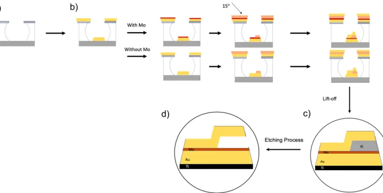
For the nanohippos structures we had four different configurations. Where two of the samples had a 1 nm layer of Mo and the other two had no Mo, within the samples we also made a variation in the cavity and consequently the overhang had to follow the change. We started by firstly, depositing 2 nm of Ti in the Si/Glass substrate to ensure adhesion, at a rate of 1 Å/sec, followed by a 30 nm layer of Au at 1 Å/sec as well, in all samples. Afterwards, in two samples was
11
added 1 nm of Mo at 0.1 Å/sec. Proceeding on the protocol, in one structure with Mo and another with no Mo, a 10 nm layer of Al was deposited using a 15° angle at a rate of 0.6 Å/sec with a 20 nm Au layer on top at 1 Å/sec. For the other two samples, the same conditions were used however the Al layer was 20 nm and the Au on top 30 nm thickness. The final schematic can be observed below in FIG. 6. Note that all the samples were rotating at 3 rpm to ensure homogeneity except the Al layer with a 15° degree angle.
3.1.6. Samples Development and Etching Process
Lift-off process was used, using acetone and then rinsed with Isopropyl Alcohol (IPA). Finally, they were dried using compressed N2.
For the etching process, the sample was put into a tine with etchant (TechniEtch Al80) for 20 minutes, then transferred into deionized water for a couple of minutes and finally dried with N2.
3.1.7. Oxygen Plasma Treatments
All the cleaning and PMMA etching were carried out on Vision 300 MK II, Advanced Vacuum. The process parameters are described on table 1.
Table 1: Oxygen plasma treatment parameters for all processes.
Step Time (min.) RF power (W) Process pressure (mTorr) O2 flow (sccm) Cleaning procedure 10 100 25 40 PMMA etching 8 50 25 40
FIG 6: General schematic of the nanohippos fabrication, starting with a Au layer deposition, followed by Mo (in the upper configuration). A Al sacrificial layer is added with a 15 degree angle and finally the top layer of gold.
a)
b)
12
3.1 Characterization Techniques
3.2.1. Scanning Electron Microscopy
The structures’ morphology was analysed via SEM (Magellan 600 from FEI). The working distance was between 4 and 6 mm, a working potential of 10kV and a nominal beam current of 25pA. Image J was used afterwards in order to obtain data related to the structure’s distribution sizes.
3.2.2. Atomic Force Microscopy
Additionally, AFM (Edge from Bruker) was used to further analyse the nanohippo structure’s morphology, and a 2D surface imaging and the roughness profile have been obtained, relevant for the confirmation of a step difference on top of both structures. Gwyddion was used for the data analysis.
3.2.3. X-Ray Photoelectron Spectroscopy
XPS Kratos Axis UltraDLD (Kratos Analytical Ltd. Telford, UK) equipped with a
monochromated Al 𝑘G X-Ray source (hv=1486.6 eV), base pressure of 1x10⁻⁹ Torr, operating at 1 0kV and 15 mA (150 W), pass energy of 50 eV for survey spectra and 20 eV for High Resolution (HR) spectra, was used to measure the elemental composition of our sample’s surface. The Binding Energy (BE) scale for all spectra was calibrated by assigning C-C/C-H component in the C 1s spectra to the BE of 284.8 eV. Note that all samples were analysed right after the procedure was finished in order to avoid air contaminations. CasaXPS software was used for data analysis.
3.2.4. Extinctions Measurements
Extinction spectra were obtained using a spectrometer (Shimadzu UV-3600 UV-VIS-NIR). Dual beam measurements were performed with a clean glass slide as a reference, the samples were facing the light source and the extinction was measured on the backside of the substrates.
3.2.5. FDTD Simulations
The simulations were obtained from finite-difference time-domain (FDTD) calculations performed in a commercial software (Lumerical Solutin, Inc., Canada). The overall simulated structures were composed by two structure groups, one for the cavity and another one for the nanostructure. The nanostructure was composed by three truncated cones, with dimensions and optical constants stated on table 2. The structures were simulated on top of a “Object defined dielectric” with an index number of 1.52, reproducing a glass substrate, in a vacuum background with a refractive index of 1. It was used a total-field scattered-field as a source from a vertical direction and the electrical field was aligned along with the x-axis. The mesh size was 5nm for x and y direction and 6nm for z direction, all the boundaries used were perfectly matched layers (PML). The simulations took between 10 and 12 minutes. All the simulation process and specifications are described in Annex 5.
Table 2: Simulated structure dimensions.
Material Inferior Radius (nm) Superior Radius (nm) Thickness (nm)
Top Disk Johnson and Christy Au 67.2 60.5 50
Middle Disk Lajaunie MoO3 67.3 67.2 1
Bottom Disk Johnson and Christy Au 70 67.3 20
14
4. Results and Discussion
The desired structure are schematically depicted in FIG. 7 below, it presents a 140 nm diameter a bottom Au layer of 30 nm, 1 nm of Mo (when used), 10 nm of Al with 20 nm of Au on top or 20 nm of Al with 30 nm of Au on top. The 140 nm diameter was the best compromise between a bigger area structure to interact well with light and the non-collapse of the overhang. I.e. the final objective would be a structure with a plasmonic high field region, inside the cavity, in which a 2D material or dielectric could be placed. The nanofabrication used, also allows applications to larger areas.
FIG 7: Schematic cross section of the final structure after the etching step. A) The structure with 1nm of Mo and B) with no Mo.
FIG. 8 corresponds to SEM images of two different samples of previous structures with a
300 nm diameter with a collapsed overhang.
FIG 8: SEM images of nanohippos with a bottom diameter of 300 nm and A) with a 10 nm cavity with also, 10 nm Au layer on top and B) 20 nm cavity with 30 nm of Au on top.
The obtained structures were morphological and chemical characterized through the techniques later presented.
4.1. Scanning Electron Microscopy
FIG. 9A and 10A show the mentioned 140 nm plasmonic nanostructures prepared by
HMCL, dispersed on a silicon substrate, after lift-off process and before the etching of the Al (see
FIG. 6c)). By the observation of the data the efficiency of the mask pattern made by HMCL can
be verified, since the nanostructures are evenly distributed with no agglomeration visible as a result from the electrostatic repulsion between the nanoparticles. A step difference on top of our structure is also noticeable, due to the deposition of Al. The deposition of the material in one side of the structure will increase the thickness on half of the structure, creating the mentioned step difference, visible at FIG 9A and 10A and later confirmed by AFM analysis. Besides the step difference, it is also evident in the SEM images a deposit of Al on the side of the nanostructure
15
(highlighted in red), due to the fact that Al is evaporated by an angle sticking itself to the Silicon surface.
The nanoparticle distribution is presented in FIG. 9B and 10B and was obtained through imageJ software. It should be noted that the measurement used for the particle size analysis is the Feret’s diameter, which is a measure of an object through the longest direction [34], considered to serve as a good approximation for the obtained spherical nanoparticles. By the observation of the graphs it can be concluded that, in fact, there is a variation in the particle’s size, the contrary would not be expected due to the nature of the mask fabrication, HMCL. Besides that, in FIG. 9B most particles are between 120 and 125 nm this is probably because the software used did not took into account the Al side deposition. While in FIG. 10B most particles are between 140 and 150 nm leading to conclude that in this case, the Al was taken into account for the Feret’s diameter measures.
FIG 9: 140nm PSNPs spread over a silicon surface A) With a 10 Al layer and a 20nm Au layer on top and B) the respective size distribution of the nanoparticles. This image was obtained on a silicon
substrate.
FIG 10: 140nm PSNPs spread over a silicon surface A)with a 20Al layer and a 30nm Au layer on top and B) the respective size distribution of the nanoparticle. This image was obtained on a silicon
substrate.
The final structures shown below in FIG. 11 and 12 were obtained after removing Al with an etchant (see FIG. 6d)). These figures show samples with a cavity originated from the etching of the Al layer. It is also possible to note some defects that can occur during the structures’ fabrication, such as: not all structures form a defined cavity, the said cavities show different sizes suggesting that the etching process was not fully completed. On the other hand, the structures do not present all the same size, such result is unavoidable due to the nature of the mask fabrication, as mentioned above (FIG. 9B and 10B). The HMCL may also be the reason for some structures not presenting a cavity, caused by a shrinking of the hole while depositing material by PVD (see reference [35] and Annex 1). By further decreasing our structures’ diameter it could be
16
possible that the final layer of Au would only be deposited on top of the Al layer, causing the loss of the top of the cavity during the etching process.
FIG 11: Side View SEM picture of the final nanohipppos structures after removing the sacrificial Al layer with Al etchant. Here is presented a 20 nm cavity and an overhang of 30 nm of Au. At A) we had an
etching time of ten minutes and on B) an etching time of twenty minutes.
FIG 12: Side view SEM picture of the final nanohippos structures after removing the sacrifitial Al layer with etchant. Here it is presented a 10 nm cavity and an overhang of 20 nm of Au. in A) the sample
17
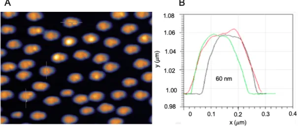
4.2. Atomic Force Microscopy
Additionally, AFM was used to further analyze nanohippo’s structures morphology, confirming the step difference due to the sacrificial Al layer as well as the height of the structures. As predicted, the FIG. 13, corresponding to the first configuration (30 nm Au in the bottom and 20 nm of Au on top of 10 nm of Al) presents a height of around 60nm and the second configuration (30 nm of Au in the bottom and 30 nm of Au on top of 20 nm of Al), FIG. 14, shows a height of approximately 80nm.
FIG 13: AFM scanning result from nanohippos samples with 2um2 A) AFM image of the nanohippos
with a 20nm Au layer on top of 10nm Al layer and B) height of nanohippos structures.
FIG 14: AFM scanning result from nanohippos samples with 2um2 A) AFM image of nanohippos
18
4.3. X-Ray Photoelectron Microscopy
The analysis of surface chemistry was performed through XPS. The study was applied to
several samples in order to clarify some concepts.
Firstly, we started by wanting to know if, indeed, we had Mo in the nanohippo’s structure. For that, two samples were prepared under the same conditions, the first one had 30 nm of Au under 1 nm of Mo and the second one was 30 nm of Au in the bottom, 1 nm of Mo and a 20 nm of Al on top. The resulted spectra are presented in the following FIG. 15 and 16, representing a plot of the number of electrons detected (Y-axis) versus the binding energy of the electrons detected (X-axis) on a range of approximately 10 nm from the surface´s sample. In FIG. 15, it can be observed the peaks corresponding to Au, Mo, Carbon and Oxygen and, from the atomic quantification, it can be detected a reasonable amount of all the elements. Both Oxygen and Carbon arise from inevitable contaminations from the air. Although Oxygen may also come from the oxidized states of Mo (MoO2 and MoO3), it is also important to note that, although the samples
contain 30 times more Au than Mo, Mo is presenting a higher percentage than Au, this can be explained by the operation principle of XPS. XPS only detects the electron that can escape from the sample and reach the detector, in order to escape from the sample, a photoelectron must travel through the sample. However, this photo-emitted electron can undergo collisions, recombination and trappings within the material, resulting in a reduced number of escaping photoelectrons. These effects appear as an exponential attenuation function as the depth increases (see annex 2), making the signal from the top layers much stronger than the signal detected from a deeper region of the sample [36,37].
19
FIG 16: X-Ray photoelectron spectroscopy survey spectra of a homogeneous film with a Au bottom layer, Mo in the middle and A) on top Al before the etching step B) after the etching of Al.
An identical image analysis can be made for spectra in FIG. 16. The data extracted from the survey spectra presented in FIG. 15 and 16 shows that Mo is not present in the sample after the etching process of the Al layer. To note that in FIG. 16A Mo does not appear in the survey spectrum because it has a 20 nm Al layer on top reaching the maximum range analysis of XPS
(~10 nm).
Proceeding, two scenarios might have happened along the process, 1) Mo is not etch resistant to the Al etchant or 2) Mo may have diffused onto the gold layer while depositing the metals by PVD due to the high temperatures of the process. To investigate these two options, further XPS analysis were made.
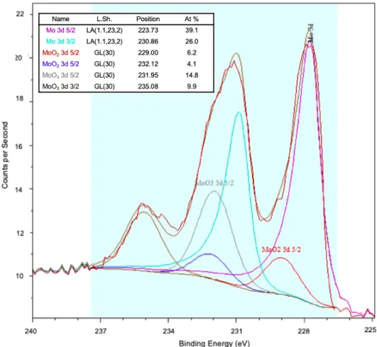
From this experiment, it was also possible to analyse the Mo by a high resolution (HR) spectrum (FIG. 17) in order to identify the chemical shift and the valence state of the Mo, while the survey spectra gives only the elemental composition and quantification. A fitting of components and regions was made by CasaXPS resorting to the information in Annex 3 with a defined space between the peaks (∆) of 3.13, in order to analyse the oxidised states present in the sample. The analysis was also made taking into account that Mo is a doublet, a doublet transition consists in the split into two states of the final state due to unpaired electrons with respect to orbital and spin angular moment, resulting in the splitting of the energy levels [38], being that the reason for the two peaks for each state in FIG.17.
It can be verified that MoO2 and MoO3 are present, given the peaks at 229 and at
approximately 232eV respectively (according to the literature [39], Annex 3) and an atomic percentage of 65.1 for metallic Mo, 10.3 for MoO2 and finally a 24.7 for MoO3. To note that under
the X-Ray beam MoO3 may be reduced, this effect is accentuated if the power used in the beam
is very high (in this case 150W was used, not considered high), MoO2 on the other hand is quite
20
FIG 17: Peak fitting of Mo compounds.
This next experiment was conducted in order to check if the Mo was diffusing into the gold layer during PVD step when Mo is deposited. Given the fact that, Mo is a refractory metal and evaporates at high temperatures, potentially could have been diffused into the Au layer. To test this hypothesis, four samples of homogeneous films were analysed, all of the samples containing a top layer of 1 nm of Mo and a Au layer in the bottom with, 10, 30, 50 and 100 nm, respectively. The expectation would be that if the Mo is diffusing into the Au it would be progressively more diluted as the amount of Au increases leading to a lower detected amount of Mo at the surface. The results can be observed below in FIG. 18.
21
FIG 18: XPS spectra corresponding to the homogeneous films A) 10nm Au with 1nm Mo on top, B) 30nm Au with 1nm Mo on top, C) 50nm Au with 1nm Mo on top and D) 100nm of Au with 1nm of Mo on
top.
By the analysis of the resulted spectra, it is possible to acquire the information about the amount of Mo in our sample in the following table 3:
Table 3: Atomic percentage of Mo according the different Au thicknesses.
Au thickness (nm) Mo Atomic percentage (%)
10 27,5
30 30,9
50 27,0
100 9,8
The results suggest that there is no diffusion of Mo into the Au layer, since the amount of Mo in each sample does not vary significantly. It is likely that Mo was, indeed, etched away by the Al etchant. To note that for 100 nm Au layer the amount of Mo detected decreases significantly, this does not fit along with the previous results, suggesting that something might have gone wrong in the PVD process or in the XPS analysis when doing the sample preparation, or when preparing the conditions in the XPS software, such as poor acquisition process. Or even technical problems with the equipment.
Further experiments were made to check if the diffusion of Mo into and through Au happens when the structure is heated [33]. For that a tri-layer disk was fabricated with the following configuration: 50nm Au- 1nm Mo- 10nm Au and heated for 1 hour at 400° C in a furnace chamber. The resulting spectra is depicted below (FIG. 19), and the respective HR spectra can be found in
Annexe 4. From the survey, it can be concluded that the Mo is ‘pulled out’ of the Au top layer into
22
FIG 19: XPS survey spectra of the tri-layer disk with 50nm of Au-10nm of Mo and 10nm of Au on top, with a heat treatment of 1h under 400° degrees.
23
4.4. Extinction Measurements – Experimental and
Simulations
The following experimental spectra may contain some discontinuities at approximately 850nm generated by the changing of the grating system in the equipment, in order to access different spectral range, this should be ignored.
In FIG. 20, the UV Vis extinction spectra is shown for the structures before the etching step (no cavity yet) for the different configurations. Each of the configurations, have a high absorption peak at a specific wavelength. The samples with Mo for a 10 nm and 20 nm cavity will correspond to a wavelength value of 628 and 613 nm respectively while the samples without Mo have a wavelength of 627 nm for a 10 nm cavity and 626 nm for a 20 nm cavity.
FIG 20: Extinction spectra for the nanohippos before the etching process, for the 4 different configurations. In black it is presented the structure without Mo and 30nm of Au on top of 20nm of Al, in
blue no Mo 10nm of Al beneath 20nm of Au. In red and green curves we have a 1nm layer of Mo and 20nm of Al underneath 30nm of Au and 10nm of Al over 20nm of Au respectively.
The difference in the peak position should be due to the increase of ,diameter/height, aspect ratio, leading to a red shift on the spectra (peak shifts to higher wavelengths). We can also note that the different samples present different intensities, that being explained by the amount of Au present on the sample, a lower signal will be related to a lower concentration of structures on the sample. Below 500 nm the spectra displays an increasing of absorbance which corresponds to the Au interband transition that are quite predominant below this wavelength. Although not relevant for the study of the extinction spectra, this part of the graph indicates which sample has more Au in it, since more Au will lead to a bigger interband absorption. As expected the samples with the extra 10nm of Au (30Au-20Al-30Au) present a higher interband transition.
Furthermore, in FIG. 21 Al have been etched away and at this point a cavity should be present, as seen in the Si samples. Nonetheless, a smaller peak for higher wavelengths does not appear as the extinctions measurements in the simulations suggested (FIG. 22 and 23).
24
FIG 21: Nanohippos extinction spectra after an etching process of A) 10 minutes and B) 20 minutes for the 4 different configurations.
Following the experimental results, two simulations were made: one with MoO3 and another
without MoO3 layer for a 20 nm cavity.. The following graphs (FIG. 22 to 24) display the scattering
cross-section of light interacting with the structure. Each spectrum shows two peaks: a high intensity, high energy (HE) peak that is insensitive to the dielectric layer and a low energy (LE) one.
The nature of the resulting modes, the wavelengths resonances and respective widths, as well as the enhancement magnitude of the electrical field are mainly dependent on the shape, size and features of our structure, such as, appearance of a cavity and the absence or not of a dielectric layer. To note that, for the Mo configuration simulation, an over mesh was used with a 1 nm refinement in the z direction for the detection of a thin 1 nm layer of MoO3.
The simulated spectra in FIG. 22, corresponding to the Mo configuration, displays a HE peak at 667 nm and a LE for 898 nm. Both peaks correspond to a resonance plasmonic peak for a specific wavelength whereas the electric field is enhanced. However, the first peak corresponds to a dipole resonance of the nanoparticles where the electrical field is outside the structure (FIG.
26) while the smaller one simulates a cavity mode (FIG. 25).
Proceeding to the comparison with the experimental data, we can conclude that there is a small blue shift (i.e. shifts for lower wavelengths) in the primary plasmon mode (HE peak) since the simulated spectra presents its peak at a slightly higher energy (613 nm). The disagreement between the experimental and simulated data is potentially due to an overestimation of the refractive index of the materials in the simulation or differences in the geometry and dielectric properties.
25
FIG 22: A) Simulated extinction spectra for one nanohippo structure with a MoO3 layer (highlited in
red), a 20nm cavity and a 30nm au top layer and B) the simulated refractive index corresponding to the nanohippo.
FIG 23: A)Simulated extinction spectra for one nanohippo structure without MoO3 layer, a 20 nm cavity and a 30
nm Au top layer and B) the simulated refractive index corresponding to the nanohippo.
In FIG. 23, it is shown the simulated spectrum for a nanohippo with no Mo. A HE peak is presented at 668 nm and a LE peak at 939 nm. Overall, both the simulation and the observed data features a HE peak mode that is constant in intensity and spectral position with or without a dielectric layer. For the LE peak, it was not observed in the experimental data and some of the causes that may have contributed for it will be explained later on.
Comparing the simulated spectrum, FIG. 24, it can be seen a shift of the LE peak (of 26 nm) for higher energies, due to the confinement between the two metal surfaces. Frederiksen et al. in 2013 also showed that by increasing the dielectric gap between the conductor layers, would lead to a linear blue shift of the LE peak [41].
26
FIG 24: Simulated extinction spectra for both structures with (in black) and without MoO3 layer (in red).
The differences between the experimental and the theoretical results suggest that the nanostructure geometry variability, mentioned above, are more predominant than what would be expected, heavily influencing the appearance of the smaller peak at longer wavelengths, since different size particles will oscillate in different wavelengths flattening the peak till it is no longer visible in the practical situation. Given the fact that the simulation only deals with one structure while the actual experimental structures will present some variability. Another possibility could have happened, such as an agglomeration of the nanostructures leading to an absence of the plasmonic effect, however a 2 nm Ti film was deposited on top of the glass samples and subjected to an SEM analysis (see Annex 6) concluding that no significantly agglomeration was present in the glass samples.
27
4.5. FDTD Simulations
Simulated electric field plots were extracted for the LE and HE mode, for both nanohippos configurations (with and without MoO3 layer), in order to investigate how the modes behave under
illumination. The near-field plots are extracted along x,y and z-planes, having into account that the light is injected perpendicular to the x-plane and the electrical field is aligned perpendicular to the source direction.
Starting by generally analysing the nanohippo with a dielectric layer for both wavelengths, it can be seen that in FIG. 25 (corresponding to the LE peak) the field enhancement is inside the cavity and in the dielectric region mainly. While for FIG. 26, the enhancement is centred in the sharp edges of the nanostructure due to the single behaviour of the electrical field near the edges. By further analysis, in FIG. 25 B) and C) field plots, it can be concluded that we have a cavity mode, since the electrical field is established inside the cavity, leading to opposite charges on opposite sides of the cavity, creating the movement of the electron from the upper side of the structure to the bottom side through the structure. Nonetheless, by observation of FIG. 25 A) and
B) the electric field enhancement of the LE mode is mainly confined to the dielectric layer,
corresponding to a gap mode. Since we have a dielectric between two metal layers and it has been shown that in systems, as the one used, conductor-dielectric-conductor, that the modes are tightly confined within the dielectric gap. This plasmon modes are due to plasmon hybridization between the two interfaces, leading to a high electrical field inside the dielectric core [42–45].
Taking a closer look at FIG. 26 it is noticeable, by looking at B) and C) plots from the same figure, a dipole is present, in agreement with the HE mode observed in the extinction spectrum above.
Overall, it can be concluded that the structure presents an enhancement of the electrical field. However, the electrical field magnitude increases further if the photons are more confined, that is, in other words, that by decreasing the cavity height we would have a higher enhancement of the electric field inside the cavity.
28
FIG 26: Electrical field plots obtained for a 913nm wavelength in the A) x-component, B) y-component and C)
z-component.
FIG 25: Electrical field plots obtained for a 668nm wavelength in the A) x-component, B) y-component and C)
29
Proceeding on the field plots analysis, in FIG. 27 and 28 we have the magnitude of the electrical field for a nanohippo with no MoO3 layer. The same analysis can be made in respect to
the dipole for higher energies (shorter wavelengths) and the presence of a cavity mode for longer wavelengths. However, a gap mode is not visible in this case, as expected, since there is no gap or dielectric to confine the plasmon modes.
FIG 27: Electric field plots obtained for a 939 nm wavelength in A) x-plane, B) y-plane and C) z-plane.
FIG 28: Electric field plots obtained for a 668 nm wavelength in A) x-plane, B) y-plane and C) z-plane.
30
5. Conclusions and Future Perspectives
This project intended to develop a new plasmonic structure with the perspective to integrate 2D materials inside the cavity for enhancement of optical properties. So far, the engineering process has shown promising results since it was possible to confirm the cavity through the characterization processes. Nonetheless, the extinction measurements did not match with the simulations and the next step should be to decrease the bottom layer of Au from 30 nm to 20 nm in order to avoid the possible lack of support of the overhang due to the shrinking of the holes. Another possibility could be to use a different nanofabrication technique, one that would guarantee more uniformity of the size holes, such as electron beam lithography (EBL). This technique makes possible the fabrication of high resolution nanostructures with nanometric features, however it is a more expensive fabrication with a larger time consuming.
Furthermore, in the attempt to integrate Mo into our cavity the XPS data showed that the Mo was etched away by the Al etchant, the simplest solution would be to use another sacrificial material such as Ti, for example. In the HR XPS spectra, the homogeneous film Au-Mo showed some oxidised states, such as MoO2 and MoO3, if it had been possible to mobilize the material
inside our cavity the fabricated structure would exhibit photochemical and catalytic properties [46] due to the Mo oxides. Such properties are of high interest for several applications, including catalysis and photocatalysis [47]. To investigate deeply the materials in the cavity and the future trail materials, a TEM-EDS could be used to identify the elements across de side-view image of the sample or even resorting to the XPS depth profile.
Finally, more simulations with more complex features can be made in order to achieve a model closest to the reality. Nonetheless, the structures showed promising results and the next step should be decreasing the height of the plasmonic nanocavity in order to increase the local field even more. The resulted data displays great potential for moderately high fields and high refractive index sensitivity which can be used in sensors and biomedical applications such as photothermal cancer treatment.
The final step would be the direct integration of a 2D material on the plasmonic nanostructure, resorting to the diffusion of Mo through the Au by the use of temperature. With the unique properties of 2D materials, in particular the photoelectric characteristics of transition metal dichalcogenides and the enhancement of their properties arising from the LSPR. This final step, was not possible due to a broken machine, however it would allow many more possibilities for higher performance applications such as bio and chemical sensors, photovoltaics and others.