Sofia de Lemos Henriques Ferreira
Licenciada em Ciências de Engenharia Física
Dissertação para obtenção do Grau de Mestre em Engenharia Física
Microelectromechanical Systems
Fabrication and Characterization of Microcantilevers
Orientadores: Kjeld Pedersen, Presidente do Departamento de Física e Nanotecnologia, Universidade de Aalborg
Ana Cristina Silva, Professora Auxiliar, Universidade Nova de Lisboa
Júri:
Presidente: Doutora Maria Isabel Simões Catarino Arguente: Doutor Luís Miguel Nunes Pereira
Microelectromechanical Systems - Fabrication and Characterization of Microcantilevers
Copyright © Sofia de Lemos Henriques Ferreira, Faculdade de Ciências e Tecnologia, Uni-versidade Nova de Lisboa.
Acknowledgements
First and foremost, I would like to thank my research supervisor, Professor Kjeld Pederson for his guidance and advice, and his enthusiasm throughout the entire project. I would also like to thank Professor Ana Cristina Silva for her encouragement, support and advice.
In addition, a thank you to Peter Kristensen and Deyong Wang, who not only assisted me with some steps of the fabrication and characterization process, but also helped me to overcome all the hardships found during the experiments.
Most importantly, I would like to thank my parents for all the encouragement and unconditional love that made all of this possible.
Abstract
Microelectromechanical systems (MEMS) technologies can be used to produce from the sim-plest structures to the most complex devices and systems. Due to their many applications in various fields, MEMS have turned into one of the most researched areas in microtechnology.
In this context, this project was developed in an attempt to produce one of most used structures in MEMS sensing devices - microcantilevers. Several microfabrication techniques were combined to fabricate this type of structures on the top layer of silicon of a silicon-on-insulator (SOI) wafer.
Resumo
Sistemas microelectromecânicos (MEMS) constituem uma das tecnologias que permite produzir desde as estruturas mais simples até aos dispositivos e sistemas mais avançados e complexos. Estes sistemas têm inúmeras aplicações em diversas áreas de estudo e, por esta razão, os MEMS tornaram-se numa das áreas mais pesquisadas na microtecnologia.
Neste contexto, este projecto foi desenvolvido numa tentativa de produzir uma das mais simples e mais usadas estruturas que se podem encontrar em dispositivos sensoriais do tipo MEMS -microcantileveres. Diferentes técnicas de microfabricação foram combinadas de modo a fabricar este tipo de estruturas numa bolacha do tipo silicon-on-insulator (SOI).
Preface
This master’s thesis was written at the Department of Physics and Nanotechnology at Aalborg University, Denmark, in the spring semester of 2014. The purpose of this thesis was to fab-ricate microcantilevers structures on a silicon-on-insulator wafer and to verify their viability. Therefore, the main theme of this thesis is microfabrication and characterization. The thesis was written under the supervision of Professor Kjeld Pedersen, Head of Department at the Depart-ment of Physics and Nanotechnology at Aalborg University, and Professor Ana Cristina Silva, Professor at Faculdade de Ciências e Tecnologia, Universidade Nova de Lisboa.
Reading Guide
Throughout the report, the references to different sources will be found on the form [#], where the number in the square brackets refers to a specific source in the bibliography at the end of the report. In the bibliography, the sources will be listed with their title, author, and other relevant information depending on whether the source is a book, article, or a web page.
Contents
List of Figures xv
List of Tables xvii
1 Introduction 1
1.1 Purpose of the Project . . . 2
2 MEMS: An Introduction 3 2.1 What Are MEMS? . . . 3
2.2 Silicon as a MEMS Material . . . 6
3 Theory 9 3.1 Basic Mechanics . . . 9
3.2 Microcantilever Sensors . . . 15
4 Fabrication Techniques 17 4.1 Direct Write Electron-Beam Lithography . . . 17
4.2 Etching . . . 21
5 Fabrication and Characterization of the Microcantilevers 27 5.1 Electron Beam Lithography . . . 28
5.2 Reactive Ion Etching . . . 30
5.3 Wet Etching . . . 30
5.4 Characterization of the Microcantilevers . . . 31
6 Experimental Results and Discussion 33 6.1 Reactive Ion Etching . . . 33
6.2 Wet Etching . . . 37
6.3 Characterization of the Microcantilevers . . . 40
7 Conclusions and Future Perspectives 45
List of Figures
2.1 (a) Microcantilever bending due to a biomolecular interaction between a receptor molecule and its target. (b) Optical detection system for measuring microcantilever deflections [9]. . . 4 2.2 Typical schematic of a strain gauge sensor [12]. . . 4 2.3 (a) Parallel plate configuration for capacitive sensing, where one of the electrodes is
placed on a flexible diaphragm while the other electrode is attached to the substrate. (b) Comb structure for capacitive sensing [12]. . . 5 2.4 Schematic of an electrostatic actuator, consisting of a microcantilever on which a
micromirror is placed. [10]. . . 6 2.5 (a) U-shape and (b) V-shape actuators [11]. . . 6 2.6 Crystal orientation and dopant types in commercial silicon wafers [15]. . . 8
3.1 Prismatic bar subjected to an axial force, showing the resulting length change. Mod-ified from [17]. . . 9 3.2 Schematic of Poisson’s ratio, showing the resulting axial elongation and lateral
con-traction when a prismatic bar is subjected to an axial force. Modified from [17]. . . 10 3.3 Schematic of (a) a cantilever with a concentrated upward force acting at the free end
and (b) the resulting deflection curve. Modified from [16]. . . 11 3.4 Deflection curve of a cantilever beam with a concentrated upward force acting at the
free. Modified from [16]. . . 11 3.5 Deflection of a cantilever beam due to a uniform load. Modified from [16]. . . 13 3.6 Cantiliver beam subjected to a single load at its free end. Modified from [16]. . . . 14
4.1 Schematic of an SEM system [24]. . . 18 4.2 Schematics of (a) a thermionic electron source and (b) a field-emission electron
source. Modified from [23]. . . 18 4.3 (a) Raster and (b) vector scan systems. Modified from [25]. . . 20 4.4 (a) Perfectly isotropic, (b) partially anisotropic and (c) perfectly anisotropic etch
profiles. . . 22 4.5 Comparison between a (a) convetional etching technique and the (b) liftoffand (c)
enhanced liftofftechniques. Modified from [27]. . . 23
List of Figures
5.1 Illustration of the several steps in the fabrication of microcantilevers. (1) Deposition of a PMMA film on top of the SOI wafer. (2) E-beam writing of the microcantilevers structures. (3) Development of the PMMA. (4) Reactive ion etching of the silicon. (5) Removal of the remaining PMMA. (6) Wet etching of the buried oxide under the top silicon layer. . . 27 5.2 Schematics of the two different microcantilever structures written during the
lithog-raphy process. The light grey areas represent the areas of the PMMA film exposed during the process, while the dark grey stand for the top silicon layer. L stands for the microcantilevers length and a for their width. . . 28 5.3 Etching profiles obtained with the RIE of the silicon (a) before and (b) after the
removal of the PMMA layer. . . 30 5.4 Schematic of the set-up used to measure the current as a function of the voltage
applied between the SOI layer and silicon substrate. . . 32
6.1 (a) SEM image of sample 1. (b) Dimensions of the microcantilevers. . . 34 6.2 (a) SEM image of sample 2. (b) Dimensions of the microcantilevers. . . 35 6.3 (a) SEM image of sample 2, where the dark grey areas are silicon and the light grey
area is the exposed buried oxide. (b) Etching profile of the microcantilevers after the reactive ion etching of the silicon top layer. . . 36 6.4 SEM image of sample 2 (a) before and (b) after the wet etching of the buried oxide. 38 6.5 SEM image of sample 2 after the wet etching of the buried oxide, where it is possible
to inspect the contour line on one of the corners of the structure, which shows how much oxide was etched under the silicon. . . 39 6.6 Profile of the microcantilevers of sample 2 after the wet etching of the buried oxide. 39 6.7 Graphic representation of the current as a function of the voltage applied between
the top and bottom silicon layers. (a) shows the current measurement for sample 1, while (b) shows the current measurement for sample 2. . . 42 6.8 Graphic representation of the current as a function of the voltage applied between
the top and bottom silicon layers for sample 1. (a), (b), (c) and (b) show the current measured in 50, 100, 200 and 300 points, respectively. . . 43 6.9 Graphic representation of the current as a function of the voltage applied between
the top and bottom silicon layers for sample 2. (a), (b), (c) and (b) show the current measured in 50, 100, 200 and 300 points, respectively. . . 44
List of Tables
2.1 Silicon properties (T=300 K) [10,13,14]. . . 7
5.1 Parameters of the SOITEC wafer used in this project [32]. . . 28
Introduction
1
"What are the possibilities of small but movable machines? They may or may not be useful, but they surely would be fun to make."
Richard Feynman, 1959
Microelectromechanical systems (MEMS) are microscopic devices present in our everyday lives. They are fabricated using integrated circuit (IC) processing techniques and have dimensions in a range of a few micrometres to millimetres and combine electrical and mechanical components. These systems can sense, control and actuate on the micro scale and function individually or in arrays to generate effects on the macro scale. Applications of MEMS devices are being
devel-oped in several fields, ranging from the automotive industry to medicine, space, pharmaceutics, bioengineering, and many other fields.
In 1959, physicist Richard Feynman gave his famous lecture, "There’s plenty of room at the bot-tom" [1], where he introduced the possibilities of fabricating materials and devices at a smaller scale. In his lecture, Feynman described the amount of space available on the microscale, stating that "there is enough room on the head of a pin to put all of the Encyclopaedia Brittanica." In order for this to happen, he pointed out that it was necessary to create a new class of miniaturized machines to manipulate and measure the properties of microstructures.
The historical background of MEMS, however, goes back to the 1940s, with the invention of the transistor at Bell Telephone Laboratories in 1947, which led to a fast-growing microelectronic technology. In 1949, the ability to grow pure single-crystal silicon improved the performance of semiconductor transistors, but it was only in 1960 that the reliability and cost of these devices were satisfactory, due to the invention of the planar batch-fabrication process. This invention also permitted the integration of several semiconductor devices into a single piece of silicon thus marking the beginning of the IC industry. In 1982, Kurt Petersen drew the attention to the possibilities that MEMS offered with his paper "Silicon as a mechanical material" [2], where
he discussed the development of many micromechanical devices. Since then, there has been a tremendous increase in the number of MEMS devices and applications, as well as in the number of instruments required to produce these devices [3].
pos-1. Introduction
sibilities of implementing MEMS in places where larger devices do not fit, such as engine of cars or even inside the human body. MEMS fabrication is low cost due to batch fabrication techniques. Additionally, they consume very low power, which reduces the operational cost and allows the development of long-life and self-powered devices. Moreover, MEMS technology have enabled many smart functionalities and superior perfomances that cannot be achieved with other technologies, such as ultra-sensitive mass detectors, high-temperature pressure sensors, lab-on-a-chip biosensors, and many others [4].
1.1
Purpose of the Project
Due to all the favorable characteristics of MEMS and all their applications, the main task in this project is to fabricate one of the simplest and most used structures in MEMS - microcantilevers - on silicon-on-insulator (SOI) wafers. This has the purpose to optimize the microfabrication process of microcantilevers at the Department of Physics and Nanotechnology at Aalborg Uni-versity, in order to enable a posterior development of biossensors.
The microcantilevers will be created in the top silicon layer of the SOI wafer using electron beam lithography and a combination of dry and wet etching. Mechanical properties of the produced microcantilevers will be tested by applying a voltage between the two silicon layers of the SOI wafer, in an attempt to observe static bending. This project also includes an introduction to MEMS as well as the theoretical basis for understanding MEMS structures.
MEMS: An Introduction
2
2.1
What Are MEMS?
As the name implies, microelectromechanical systems (MEMS) are devices in the micro scale, where at least one of their dimensions is in the micrometre range. They use electric power for detection or actuation, or electronic components to amplify and filter signals or for controlling purposes. They are mechanical devices in the sense that they rely on some sort of mechani-cal motion, action or mechanism. Moreover, they function and are designed and fabricated as integrated systems and not as individual components, hence the word "systems" in MEMS [4].
MEMS are basically divided into microsensors and microactuators and their operation is based on transduction mechanisms, where a form of energy, such as electrical, mechanical and thermal, is converted into another form of energy. In microsensors, it is common to find more than one transduction mechanism in series to end up with an electrical signal, whereas in microactuators the series of transducting mechanisms is used to convert an electrical signal into a mechanical signal. Microsensors include inertia sensors (such as accelerometers and gyroscopes), pressure sensors, gas and mass sensors, temperature sensors, force sensors and humidity sensors. Ex-amples of microactuators are micromirrors, RF switches, microgrippers, generic force and dis-placement actuators, such as thermal bimorph actuators and comb-drive electrostatic actuators. Some of these examples are presented in the following sections [3,4].
2.1.1
Microsensors
Microsensors represent the majority of the MEMS devices developed to date as the available microfabrication techniques improve the performance, size and cost of sensing systems and, therefore, almost every physical quantity has a MEMS device especially developed or being developed to measure it. Microsensors have many applications in different areas of study. Here,
some of the most prominent microsensor technologies will be presented.
Biosensors
2. MEMS: An Introduction
or by suffering a change in its resonance frequency, with a much higher resolution than the
one achieved with macroscopic structures. The resonant frequency of microcantilevers varies sensitively due to mass loading from molecular interactions. Furthermore, the adsorption of molecules, when restricted to one of the microcantilever surfaces, induces a differential surface
stress that bends the microcantilever, caused by the forces involved in the adsorption process. The bending and changes in resonant frequency can be detected by several techniques, such as optical beam deflection, piezoresistivity, piezoelectricity, or capacitance [5-8]. Figures 2.1 (a) and (b) illustrate an example of a biosensor based on a microcantilever and an optical detection system for measuring the microcantilever deflections, respectively [9].
(a) (b)
Figure 2.1:(a) Microcantilever bending due to a biomolecular interaction between a receptor molecule
and its target. (b) Optical detection system for measuring microcantilever deflections [9].
Strain Gauges
Strain gauges are sensors that transduce a mechanical signal into an electrical signal. Figure 2.2 shows a typical strain gauge. By applying pressure to the structure where the strain gauge is attached, the dimensions of the conductor strips change and, consequently, its resistance varies. For several years, strain gauges have been integrated into diverse sensors, such as pressure sen-sors, position sensors and inertial sensors [3,10].
Figure 2.2:Typical schematic of a strain gauge sensor [12].
2.1. What Are MEMS?
Capacitive Sensors
In capacitive sensors, the transduction of a mechanical signal into an electrical signal is due to a change in capacitance caused by the motion of one of the two electrodes that compose the sensor. The simplest configuration of a capacitive sensor consists of two parallel plate electrodes, as shown in Figure 2.3 (a). However, this type of configuration usually results in a nonlinear relationship between the change in capacitance and the diaphragm deformation. To obtain larger linear sensing ranges, capacitors with interdigitated fingers, as illustrated in Figure 2.3 (b), have been used. Capacitive sensors are versatile in the sense that they can be used for measuring several quantities, such as position, force, pressure, acceleration, flow rate, and many others [3,10].
(a) (b)
Figure 2.3: (a) Parallel plate configuration for capacitive sensing, where one of the electrodes is placed
on a flexible diaphragm while the other electrode is attached to the substrate. (b) Comb structure for capacitive sensing [12].
2.1.2
Microactuators
Even though microactuators were not as developed as microsensors at the beginning, nowadays they are applied in several fields. Electrostatic and thermal actuators represent two of the most important applications of this type of MEMS and, for this reason, they are here introduced.
Electrostatic actuators
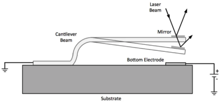
Electrostatic actuation is the most common type of actuation found in MEMS. It is based on the creation of an electric field by applying a voltage to adjacent conductors. One of the simplest examples of these actuators is a cantilever used as an optical switch, as illustrated in Figure 2.4. In this case, a laser beam is deflected by a mirror placed at the polysilicon cantilever tip. When a voltage is applied between the cantilever and the electrode placed on the substrate, the cantilever is deflected downward, shifting the mirror and rotating the deflected laser beam [10].
Thermal Actuators
2. MEMS: An Introduction
Figure 2.4:Schematic of an electrostatic actuator, consisting of a microcantilever on which a micromirror
is placed. [10].
Joule heating is lower in the cold-arm than in the hot-arm because the former has a larger cross section, leading to a decrease in electrical resistance. Thus, there is a difference in the thermal
expansion between the two arms, resulting in a rotary motion of the actuator beam. The V-shape actuator consists of one or more V shaped beams arranged in parallel. By passing a current through the beams, they heat and expand, causing the center shuttle to move in the direction of the offset [11].
(a) (b)
Figure 2.5:(a) U-shape and (b) V-shape actuators [11].
2.2
Silicon as a MEMS Material
MEMS materials include semiconductors, metals, ceramics, polymers and composites. How-ever, since the goal of this project is the fabrication of silicon microcantilevers and given the fact that silicon is still one of the most used materials, not only in MEMS technology but also in other areas of micro- and nanotechnology, this section will be focused on this material.
Silicon is the most common material in MEMS fabrication because it can be modified in various ways in order to change its electrical and mechanical properties. In addition, silicon has sev-eral sensory properties, such as piezoresistivity, thermal properties and optical properties [12]. For these reasons, many MEMS devices are fabricated in bulk silicon or in silicon-on-insulator (SOI).
2.2. Silicon as a MEMS Material
Bulk silicon from materials manufacturers has a crystallographic orientation of either 100 or 111, which means that the plane of the top surface of the produced wafers has one of these orientations. The wafers are cut on one edge to form a primary flat and in another edge to form a secondary flat, as illustrated in Figure 2.6. The relative position of the secondary flat to the primary flat informs the user about the wafer orientation and the doping type, either n-type or p-n-type. The resistivity of the wafer is given by the concentration of impurities and it can go from 0.001 to 10 000 Ω cm [14]. Table 2.1 lists some of the physical properties for
crystalline silicon. Note that some of the silicon properties are anisotropic, which means that they depend on the crystal orientation. This has to be taken into account when designing any kind of micromechanical system.
Table 2.1:Silicon properties (T=300 K) [10,13,14].
Property Value
Density 2.3 g cm−3
Lattice Constant 5.435 Å
Dielectric Constant 11.9
Bandgap Energy 1.12 eV
Electron Affinity 4.01 eV
Index of Refraction 3.42
Specific Heat 0.7 J g−1K−1
Melting Point 1415◦C
Yield Strength 7×10⁹N m−2
Young’s Modulus, (100) orientation 1.6×10¹¹N m−2
Poisson’s Ratio, (100) orientation 0.28
Thermal Conductivity 1.57 W cm−1◦C−1
Thermal Coefficient of Expansion 2.33×10⁻⁶◦C−1
SOI wafers consist of two layers of silicon separated by an oxide layer. This type of wafers can be fabricated by implanting high-energy oxygen ions into the bulk silicon, followed by an annealing process. This method, known as separation by ion implantation of oxygen (Simox), forms a buried oxide (BOX) layer at a fixed distance from the surface, leaving behind a single-crystalline silicon layer (SOI layer) as the top layer of the SOI wafer. In this process, the thick-ness of the SOI and BOX layers is limited by the range and distribution of the implanted ions. Typical values for the thickness of these layers are around 0.2µm and 0.1µm, respectively [14].
To obtain thicker layers of silicon and oxide, two silicon wafers, where at least one is covered with a thick oxide layer, are brought together, in a process known as wafer bonding. Here, the bond created between the two wafers by van der Walls forces is reinforced by a chemical reac-tion in an annealing process. One of the wafers is then thinned down by a mechanical grinding and the SOI layer is then polished. BOX layer formed via this method can have thicknesses up to 4 µm [14]. These two SOI wafers fabrication techniques can be combined to produce
2. MEMS: An Introduction
Figure 2.6:Crystal orientation and dopant types in commercial silicon wafers [15].
of the bonded wafer, the surface of the SOI layer is polished, resulting in SOI layers from 0.1 and 1.5µm and BOX layers from 200 nm to 3µm [14].
Theory
3
3.1
Basic Mechanics
To understand the design and operation behind MEMS devices, it is necessary to have a basic knowledge of the mechanics of materials. As many MEMS devices use cantilever structures, this section presents some concepts in mechanics of beams, such as stress, strain, Poisson’s ratio and beam deflection.
3.1.1
Axial Stress and Strain
When an axial force is applied to a prismatic bar, that bar will either stretch or compress. This loading force F divided by the bar cross section A gives the stress σthat the bar is subject to
[16]:
σ= F
A (3.1)
When the applied force causes the stretching of the bar, the resulting stresses are said to be tensile stresses, whereas the compression of the bar results in compressive stresses. Regarding the sign of the stress, it is considered by convention to be positive for tensile stresses and negative for compressive stresses.
Additionally, it should be noted that this equation only applies to uniformly distributed stresses over the cross section of the bar. This means that the applied force should act through the cen-troid, otherwise the bar would bend and this equation would no longer be valid.
Figure 3.1: Prismatic bar subjected to an axial force, showing the resulting length change. Modified
3. Theory
Figure 3.1 shows the change that occurs in the bar when it is subject to a tensile stress. It can be seen that the bar suffers an elongation and the ratio between the change in the length△Land the original lengthL0is called strain [16]:
ε= △ L
L0 (3.2)
Once again, if the bar is elongated or stretched the strain is called a tensile strain and it is usually taken as positive. If the bar is shorten, the strain is a compressive strain and it is taken as negative.
3.1.2
Young’s Modulus and Poisson’s Ratio
For most materials, the relationship between the axial stress and the axial strain is linear and it obeys Hooke’s law. The proportionality between these two properties is designated Young’s modulusEof a material [16]:
E = σ
ε (3.3)
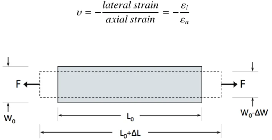
As previously stated, when a prismatic bar is in tension due to an axial force, it will suffer an
elongation in the axial direction. In addition to this deformation, the bar may also contract in the direction perpendicular to the load, as shown in Figure 3.2. Poisson’s ratioυis then the ratio
between the two strains [16]:
υ= −lateral strain
axial strain =
−εl
εa
(3.4)
Figure 3.2:Schematic of Poisson’s ratio, showing the resulting axial elongation and lateral contraction
when a prismatic bar is subjected to an axial force. Modified from [17].
Poisson’s ratio is defined as a positive value, which means that the minus sign in the equation above is necessary to compensate for the fact that usually one of the strains is negative. For example, a bar in tension will have a positive axial strain and a negative lateral strain while a bar in compression will have a negative axial strain and a positive lateral strain.
3.1.3
Deflection of beams
The most common way to find beam deflections is by finding the differential equations of the
beam deflection curve and their associated relationships. For that, a cantilever with a concen-trated upward force acting at the free end as in Figure 3.3 (a) will be considered [16]. Here, it
3.1. Basic Mechanics
(a) (b)
Figure 3.3:Schematic of (a) a cantilever with a concentrated upward force acting at the free end and (b)
the resulting deflection curve. Modified from [16].
is assumed that the plane xyis the plane of symmetry of the beam and that the force acts in this plane. This means the bending will occur also in this plane, as shown in Figure 3.3 (b).
The bending of the beam results in a deflection ν in the ydirection. Figure 3.4 illustrates this deflection at any point p1, located at distancexfrom the origin. Atx+dx, the deflection is equal toν+dνand it is represented by p2.
(a) (b)
Figure 3.4: Deflection curve of a cantilever beam with a concentrated upward force acting at the free.
Modified from [16].
Besides the deflection observed along the beam axis, there is also a rotation. The angle of rotation θ is the angle formed between the x axis and the tangent to the deflection curve at a given point. From Figure 3.4, it is clear that
ρdθ=ds
whereρis the radius of curvature,dθthe angle increment between points p1and p2 anddsthe distance along the deflection curve between the same points. Thus, the curvatureκis given by
κ= 1
ρ =
dθ
ds (3.5)
3. Theory
increment in the distancedx. Therefore, the slope can be written as
dν
dx =tanθ (3.6)
In order to simplify this analysis, small angles of rotation will be taken into account, given that the structures encountered in everyday life suffer small changes in shape while beig used and,
therefore, the deflection curves of most beams usually have very small angles of rotation. For small angles, cosθ≈1 and, consequently,ds≈ dx. Thus, Eq. 3.5 can be rewritten as
κ= 1
ρ =
dθ
dx (3.7)
Moreover, tanθ≈ θifθis small and the following approximation to Eq. 3.6 is then possible
θ≈ tanθ= dν
dx (3.8)
The first derivative ofθwith respect toxin Eq. 3.8 results in
dθ
dx = d2ν
dx2 (3.9)
Substituting this equation into Eq. 3.7 gives the relation between the curvature of the beam and its deflection for small angles of rotation:
κ= 1
ρ =
d2ν
dx2 (3.10)
If the material of the beam is linearly elastic and obeys Hooke’s law, the curvature of the beam follows [16]
κ= 1
ρ =
M
EI (3.11)
Here, M is the bending moment and EI is the flexural rigidity of the beam, where E is the Young’s modulus for the material andI is the moment of inertia of the beam.
Combining Eq. 3.11 with Eq. 3.10 results in a differential equation for the deflection curve of a
cantilever beam
d2ν
dx2 = M
EI (3.12)
Deflection Caused by a Uniform Load
Before the fabrication of the device, it is important to know the maximum deflection of the beam due to its own weight. For this purpose, a cantilever beam subjected to a uniform load of intensityq, as in Figure 3.5, will be considered.
3.1. Basic Mechanics
Figure 3.5:Deflection of a cantilever beam due to a uniform load. Modified from [16].
To start this analysis, it is necessary to find the bending moment in the beam, as Eq. 3.12 suggests. At a distance xfrom the fixed end, the bending moment is equal to [16]
M(x)= −qL
2
2 +qLx− qx2
2 (3.13)
Substituting this expression into Eq. 3.12 yields
d2ν
dx2 = 1 EI
−qL
2
2 +qLx− qx2
2
!
(3.14)
Now the first integration of the equation above gives the slope of the deflection curve
dν dx = 1 EI −qL 2x 2 + qLx2 2 − qx3 6 +C1
!
(3.15)
Here, the intregration constant can be found by applying the boundary condition that says that the slope of the deflection curve is zero at the fixed end of the cantilever,
dν
dx(0)=0
Thus, the integration constant is found to be zero and Eq. 3.15 becomes
dν
dx =− qx 6EI
3L2−3Lx+x2
(3.16)
The expression for the deflection of the beam is obtained by integrating Eq. 3.16
ν(x)=− q
EI L2x2
4 −
Lx3
6 +
x4 24 +C2
!
(3.17)
When the boundary condition that the deflection of the beam is zero at the support, ν(0) = 0,
is applied to Eq. 3.17, the integration C2 is shown to be zero. Hence, the expression for the deflection of the beam as a function of xis
ν(x)=− qx
2
24EI
6L2−4Lx+x2
3. Theory
The maximum deflection of the beam is found at the free end, i.e. x= L, and is equal to
νmax= −ν(L)= qL4
8EI (3.19)
Deflection Caused by a Single Load
When a cantilever beam is subjected to a concentrated load F at its free end, as in Figure 3.6, the bending moment at a distancexfrom the fixed end is equal to [16]
M(x)=−FL+F x (3.20)
Figure 3.6:Cantiliver beam subjected to a single load at its free end. Modified from [16].
As before, the expression for the bending moment is substituted into Eq.3.12, resulting in
d2ν
dx2 = 1 EI (
−FL+F x) (3.21)
The first integration of the equation above gives
dν
dx = 1
EI −FLx+F x2
2 +C1
!
(3.22)
Since the slope of the deflection curve is zero at the support (x =0), the integration constantC1 is found to be zero. Hence, Eq. 3.22 can be rewritten as
dν
dx = F 2EI
−2Lx+x2 (3.23)
The integration of this equation gives the expression for the deflection of the beam:
ν(x)= F
6EI
−3Lx2+x3+C2 (3.24)
Once again, the deflection at the fixed end of the cantilever is zero and, therefore, the integration constantC2is equal to zero. Thus, Eq. 3.24 turns into
ν(x)= F
6EI
−3Lx2+x3 (3.25)
3.2. Microcantilever Sensors
The maximum deflection of the cantilever beam due to a concentrated load at its free end is found at x= L:
νmax= −ν(L)= FL3
3EI (3.26)
3.2
Microcantilever Sensors
In the last decades, it has been shown by several research groups that microcantilevers are able to transduce changes in physical quantities, such as mass, temperature, heat, electromagnetic field or stress, into bending (static mode) or a change in resonant frequency (dynamic mode) [5-8].
3.2.1
Static Mode
Adsorption of molecules on one side of the cantilever leads to induced surface stresses, resulting in a static mechanical bending. In 1909, Stoney derived an expression to relate the differential
surface stress △ σ between the opposite surfaces of a thin plate with the resulting radius of curvatureρ[18]:
1
ρ = 6
1−υ
Et2
!
△σ (3.27)
whereυandE are the Poisson’s ration and Young’s modulus for the material, respectively, and t is the thickness of the plate. For a cantilever of lengthL, the deflection at its free end is equal to (see Eq. 3.10)
νmax= 1
ρ
L2 2
By combining this equation with Eq. 3.27, it is possible to obtain a relationship between the the deflection at the free end of the cantilever and the differential surface stress:
νmax=
3(1−υ)L2
Et2 △σ (3.28)
3.2.2
Dynamic Mode
When cantilevers have micro scale length and width and nanoscale thickness they are susceptible to thermal and ambient noise [5,19,20]. The resonance frequency f0of an oscillating microcan-tilever can be expressed as
f0 = 21
π
r
k
m∗ (3.29)
wherekis the spring constant andm∗is the e
ffective mass of the cantilever given bym∗
= nmb. Here, mb is the mass of the cantilever beam and n is a geometric parameter. For rectangular cantilevers,nhas a value of 0.24 [19,21]. The spring constantkis given by
k= Et
3w
3. Theory
where E is the Young’s modulus for the material and t, w and L are the thickness, width and length of the cantilever, respectively.
The adsorption of masses on the cantilever causes a decrease in its resonant frequency. By knowing the new frequency at which the cantilever vibrates, it is possible to find the change in mass that originated the respective change in the vibration frequency, through the following relation
△m= k
4π2
1 f12
− 1
f02
!
(3.31)
Here, f0 is the initial resonant frequency and f1 is the resonant frequency after the adsorption. The use of cantilevers resonant frequency to detect the presence of adsorbed masses is limited by the minimum detectable frequency shift, due to thermal limited noise [20]. The smallest detectable change in frequency can be expressed as
△ fmin = 1
A
s
f0kBT B
2πkQ (3.32)
where kBT is the thermal energy at room temperature, B is the bandwidth of the frequency spectra, Q is the quality of the cantilever resonance and Ais the amplitude of vibration. The combination of Eq. 3.32 and Eq. 3.31 gives the smallest change in mass that a cantilever can detect:
△ m= k
4π2
1 (f0−△ fmin)2
− 1
f02
!
(3.33)
It is clear from Eq. 3.32 that an increase in the quality factor and in the amplitude of vibration allows the cantilever to detect smaller frequency shifts and thus improving its sensitivity.
Fabrication Techniques
4
The fabrication of MEMS devices and structures is only possible through a combination of physical and chemical fabrication techniques, where each of them plays an important role in obtaining the desired product. The basic processes behind MEMS fabrication include most of the conventional integrated circuit process techniques, such as lithography, deposition and etching, along with specially developed micromachining techniques. This chapter presents an overview of the key processes commonly used in MEMS fabrication.
4.1
Direct Write Electron-Beam Lithography
Direct write electron beam lithography (EBL) is a patterning technique that uses a focused elec-tron beam (e-beam) to expose a resist layer, where the interaction between the elecelec-trons and the resist material leads to a change in the resist solubility. This technique offers a high patterning
resolution, especially when compared to optical lithography, since the wavelength associated with the electrons used in EBL is shorter than the wavelength of the light used in optical lithog-raphy. EBL systems were first developed in the 1960s and they can be integrated in a scanning electron microscope (SEM), where an electron beam is scanned across a surface coated with an electron-sensitive resist film [22,23]. In this project, the EBL process was carried out using this type of microscope and, therefore, a brief introduction to it is here presented.
SEM machines include a beam column, a chamber where the sample stage is located, signal detectors and a signal processing system that allows real time observation and image recording (see Figure 4.1). The column is where the electron beam is formed and controlled. It consists of an electron source, lenses and apertures, a system to deflect the beam, a blanker that turns the beam on and off, coils for beam scanning, a stigmator that corrects any astigmatism in the beam,
an acquisition system and a monitor that displays the collected and processed signal information [23,24].
The electron source is one of the most important parts in an EBL system. There are some requirements that are common to all sources: high brightness and uniformity, small spot size, good stability and a long life. There are different methods to emitt electrons. In thermionic
4. Fabrication Techniques
Figure 4.1:Schematic of an SEM system [24].
electron sources are schematically represented in Figure 4.2. Schottky emission (SE) combines these two processes, where the electrons are thermally excited and then extracted by an electric field. Electrons can also be generated by inciding light into the source (photoemission). In this case, the energy of the photons is transferred to the material electrons, where the ones near the surface are emitted as photoelectrons [10,22].
(a) (b)
Figure 4.2: Schematics of (a) a thermionic electron source and (b) a field-emission electron source.
Modified from [23].
In EBL systems, the most common source is thermionic, since it provides high brightness. This parameter is evaluated by measuring the energy of the fraction of the electrons that are emitted
4.1. Direct Write Electron-Beam Lithography
and collected. The emitted electron current density is given by
Jc = AT2exp−Ew/kBT
(4.1)
where A is Richardson’s constant for the material, Ew is the effective metal work function, T
is the temperature and kB is the Boltzmann constant. By increasing the current density, it is possible to increase the brightness. This increment, however, may not be directly proportional since an increase in the current may lead to a decrease in the collection efficiency [10].
The materials most used in thermionic sources include tungsten, thoriated tungsten or lanthanum hexaboride, LaB6. The latter is nowadays the material of choice since it provides high brightness and high current density due to its very low work function, as well as a small source size (around 10 µm). However, this material is very sensitive to high pressures and therefore requires a
vacuum between 10−7 and 10−8 torr. On the contrary, tungsten filaments can be operated in
higher pressure environments but the resulting current density and brightness are not as high. Still, this material has been chosen over the years for its ability to endure high temperatures (around 3000 K) without melting or evaporating. By using thoriated tungsten as the source material, it is possible to achieve higher current densities. This material, however, yields an even lower brightness for the same current density as tungsten filaments and requires a higher vacuum [10,22,23].
Cold field emission sources consist of a tungsten needle where the sharp point has a radius less than 1µm, which helps to create the high electric field necessary to extract the electrons out of
the material. This type of source is common in electronic microscopes but not so much in EBL systems, due to the noise caused by the adsorption of atoms or molecules to the surface of the tip. This effect has more consequences in lithography than in microscopy since the work function
of the tip material is affected and therefore the emission current suffers large variations. To
minimize this problem, the electron source needs to be operated in very low pressure conditions, with a vacuum of at least 10−10
torr [23].
In Schottky emission, also known as thermal field emission, the tungsten needle used in field emission is heated, which helps the tip to be less sensitive to the environment gases. Zirconium oxide is usually used to coat the tungsten tip in order to reduce the work function barrier. A high brightness is achieved with this source as well as a moderate energy spread [23].
Now, the diameter of the crossover of the electron beam created by the source is not small enough to produce images with high resolution. Thus, a mechanism is necessary to demagnify this diameter (10-20 µm for thermionic sources) to the final beam spot size on the sample (1
nm-1 µm). A series of electromagnetic lenses are used for this purpose for when the electrons
experience the produced magnetic field, they spiral towards the center of the lenses and therefore being focused. By increasing the current that crosses the wire coil inside the lens, the magnetic field is also increased, causing the focal point of the beam to move upwards and the beam spot size to reduce [24].
4. Fabrication Techniques
focuses the electron beam on the sample by moving it along the optical axis. Deflector coils and stigmator coils are located in this lens gap, where the former is used to raster the beam across the sample surface and the latter is used to correct the astigmatism caused by the lenses. Astig-matism happens when the beam has two different focal lengths in the perpendicular direction
due to some asymmetries in the magnetic field produced by the lenses. As a consequence, the beam diameter turns out to be larger than it should be. This can be fixed by the stigmator that applies a counter field in the xor ydirection and by that assuring that the beam has a circular cross-section. In addition, electromagnetic lenses are also responsible for aberrations that are critical in EBL systems. There are two types of aberrations, spherical and chromatic. Spherical aberrations occur when the outer zones of lens focuses more strongly the electrons than the inner zones. This can be corrected by inserting an aperture after the condenser lenses so that the elec-trons will not travel to the edges of the objective lens. On the other hand, chromatic aberrations take place when the beam contains electrons of different energies, which are focused at different
image planes. By increasing the energy of the primary beam or by using a smaller aperture, it is possible to minimize this type of aberrations. The beam current, however, is reduced by de-creasing the aperture and therefore the size of the aperture has to be optimized in order to obtain a good signal-to-noise ratio and small aberrations [23,24].
Once the beam has been focused, the deflector coils will scan the beam across the surface of the sample. There are two ways to scan the electron beam. In the first method, known as raster scanning, the beam is scanned sequentially over an entire area and the intended pattern is written by blanking offthe beam where no exposure is desired, as shown in Figure 4.3 (a). This method,
however, can take a long time to be completed, since the entire area has to be scanned. The second method, known as vector scanning, directs the electron beam to the areas to be exposed, which allows to save time (see Figure 4.3 (b)).
(a) (b)
Figure 4.3:(a) Raster and (b) vector scan systems. Modified from [25].
In EBL, the sample is coated with a resist sensitive to electrons. When a polymer is bombarded with electrons, the polymer chains are broken, turning the resist more soluble. In theory, any polymer could be used as a resist if not for the several requirements that have to be fulfilled,
4.2. Etching
such as sensitivity, tone, resolution and contrast and etching resistance. The most popular resist used in EBL is poly(methyl methacrylate) (PMMA) for it offers high resolution and it is easily
handled, having good film characteristics [22,26].
The resolution of EBL is not only a consequence of the final spot size of the focused beam; it is also affected by the broadening effects that take place during the exposure. When the electrons
first interact with the resist, they are forward scattered at relatively small angles and the beam diameter suffers a slight broadening. As the electrons penetrate into the resist and substrate,
they experience backscattering events and the area that ends up being exposed is larger than originally intended. These secondary electrons emission is therefore one of the major areas of concern in EBL since the developed patterns tend to be wider than the ones scanned, as a result of the interaction between the primary beam electrons and the resist and substrate. By increasing the energy of the primary electrons and using thinner resist layers, it is possible to minimize the forward scattering. Backscattering events do not depend significantly on the beam energy but they do depend on the substrate material, since high atomic number produces more backscattering. This effect can be controlled by lowering the dose, ensuring that the resist is not
overexposed [8,9,12].
4.2
Etching
After a pattern has been designed on the resist by the lithography process, the next step is usually to transfer that pattern into the substrate under the resist. Etching is the process that removes the desired material from the substrate, either by physical damage, chemical attack or a combination of the two. By immersing the sample in a solution, the chemical etchants will react with the exposed areas of the substrate, forming soluble by-products in a process known as wet etching. In contrast, if the substrate material is removed by etchant gases then the etching is a dry etching.
Etching processes can be characterized by several important parameters. The first one to be considered is the etch rate, which gives the thickness etched away per unit of time. A high etch rate is often desirable, though too high etch rates may turn the etching process too difficult to
control. In addition, it is important to know the etch rate selectivity, i.e. the ratio of the etch rate for the various materials being exposed in the etching process with respect to the etch rate of the material being removed. Equally important is the undercut obtained with the etching. This can be evaluated by the degree of anisotropy A, which depends on the etch rates in the vertical and lateral direction, as shown in Figure 4.4. Anisotropy is expressed as
A=1− RL
RV
(4.2)
whereRLis the lateral etch rate andRV is the vertical etch rate. From Eq. 4.2, it is clear that an ideal anisotropic etching has a value of 1 while a completely isotropic etching has a value of 0 [10,27].
4.2.1
Wet Etching
4. Fabrication Techniques
(a) (b) (c)
Figure 4.4:(a) Perfectly isotropic, (b) partially anisotropic and (c) perfectly anisotropic etch profiles.
and the whole process can be described in three basic steps: diffusion of the etchant species
to the exposed surfaces of the sample, selective and controlled reaction of the etchant with the material to be etched and transport of the by-products away from the surface. Here, the etch rate is determined by the slowest step in the process, which is called the rate-limiting step. The etchant solution is often agitated to facilitate the removal of the by-products, so that the etch rate does not suffer large variations during the etching [10].
Silicon and silicon dioxide are two of the most used the materials in MEMS fabrication and, as a consequence, the wet etching processes for these materials are well known. A dilute solution of hydrofluoric acid (HF) is usually used to etch SiO2. Different concentrations of HF can be found in the market, such as 6:1, 10:1 or 50:1, meaning for example that there is 6 parts of water to one part of HF. HF solutions have a high selectivity over silicon, typically better than 100:1. However, the silicon exposed in a SiO2etching is also etched, albeit at a much slower rate, since the surface of the silicon will be slowly oxidized by the water in the solution and consequently HF etches this oxide. Deposited oxides etch faster than thermal oxides and doped oxides etch even faster as the impurities in the oxide increase the etch rate. Moreover, etching processes using HF solutions lead to completely isotropic etch profiles [10].
In order to maintain a constant etch rate throughout the etching, a buffering agent, such as
ammonium fluoride (NH4F), is typically added to the HF solution so that the concentration of HF is kept constant during the whole process. The overall reaction for etching SiO2is [10]
SiO2+6HF−→H2+SiF6+2HF2O
The buffered reaction is given by
NH4F⇋ NH3+HF
On the other hand, the wet etching of silicon occurs via a redox reaction followed by the etching of the resulting oxide by HF. A solution of HF, nitric acid (HNO3) and water is commonly used as the etchant solution for silicon and the overall reaction is expressed as [10]
Si+HNO3+6HF−→H2SiF6+HNO2+H2+H2O
Acetic acid (CH3COOH) often replaces water as diluent in this type of etchant solutions. Isotropic etch profiles are obtained with this solution, meaning that all etch directions are etched at the same rate. Here, the etch rate is controlled by the acid that has the lowest concentration, i.e. at
4.2. Etching
low concentrations of HNO3 the etch rate is limited by the oxidant concentration, whereas at low concentrations of HF the etch rate is controlled by the etchant concentration [10].
In crystalline materials, such as silicon, a high anisotropic etching can be achieved by a fre-quently used solution of potassium hydroxide (KOH), isopropyl alcohol (C3H8O) and water. The etch rate of this solution depends on the crystalline plane that is exposed, which results in sharp etch facets with controlled angles [10,28].
LiftoffTechnique
Occasionally, there are materials, such as noble metals, that are difficult to etch via the
conven-tional wet etching methods and thus direct etching is usually replaced by the liftofftechnique.
In this technique, a resist is first deposited and patterned on the substrate. The material to be etched is then placed on top of the patterned resist and substrate, as shown in Figure 4.5 (b). By using a solvent to dissolve the resist, the material in contact with the substrate remains while the parts in contact with the resist float away in the resist dissolution or are rinsed, brushed or blown from the substrate. Although this technique offers an alternative for materials difficult to etch,
the final result may exhibit some irregular edges due to the thin layer of material deposited in the resist sidewalls before the resist removal. Enhanced liftoff, shown in Figure 4.5 (c), is often
used to minimize the sidewall deposition and therefore improving the etch definition. Here, two layers of resist are used, where the top one is more resistant to the developer than the bottom one. When both resists are exposed and developed, an overhanging region in the top resist layer is created and thus preventing the material from depositing in the resist sidewalls [27].
(a) (b) (c)
Figure 4.5:Comparison between a (a) convetional etching technique and the (b) liftoffand (c) enhanced
liftofftechniques. Modified from [27].
4.2.2
Dry Etching
4. Fabrication Techniques
(diode setup) and ion-beam etching (triode setup). In glow discharge etching, the plasma is generated in the same chamber where the substrate to be etched is placed, whereas in ion-beam etching, the plasma is created in a separated chamber from which the resultant plasma ions are extracted and directed to the substrate [22].
Plasma-assisted etching may refer to physical sputter/ion etching and ion-beam milling (IBM),
chemical plasma etching (PE) or reactive ion etching (RIE). In physical sputter/ion etching and
in ion-beam milling, there is no reaction between the plasma elements and the substrate. This process is purely physical and the substrate is etched due to the momentum transfer between the energetic ions and the substrate surface. In the case of chemical plasma etching, reactive neutrals of the plasma diffuse to the substrate, where reactions between the two occur to form volatile
products, which will be carried away from the surface and then pumped out of the chamber. Here, the plasma is only used to provide etchant species during the etching process. Reactive ion etching combines these two techniques, resulting in a chemical reaction of the reactive species with the substrate aided by the ion bombardment of the substrate [22].
Plasmas can be produced in a DC field, an AC field, or a radiofrequency (RF) field. For RF fields, a high-frequency of 13.56 MHz is typically used [22].
Reactive Ion Etching
Reactive ion etching is a plasma-assisted dry etching technique that combines the physical sput-tering of the substrate with the chemical action of reactive species. RIE systems consist of a vacuum chamber, where two electrodes are placed parallel to each other and driven by a RF power source (diode setup). As illustrated in Figure 4.6, the etchant gases are introduced into the chamber in the top and pumped away by a vacuum system located at the bottom of the chamber.
Figure 4.6:RF plasma etching system with a paralell-plate configuration.
In RIE, a RF voltage is applied between the two electrodes, causing the free electrons to oscillate and collide with the gases’ molecules in the chamber and thus creating a sustainable plasma,
4.2. Etching
which includes positive and negative ions, electrons, radicals and photons. The substrate to be etched is laid on the electrode that is capacitively coupled to the RF power source, as shown in Figure 4.6. At high frequencies, only electrons respond to the frequency changes in the electric field, since their mobility is much greater than the ions mobility. Due to the oscillation of the electrons, the capacitively coupled electrode is struck by electrons and thereby developing a negative DC bias. This creates an electric field that points from the plasma towards the electrode and the positive ions that come close to the electrode will be accelerated towards it. Thus, any material placed on the electrode will be bombarded with positive ions, in a process known as ion sputtering or ion etching. Here, the etching is due to the momentum transfer from the ions to the material’s atoms in a direction nearly normal to the surface, which guarantees high degrees of anisotropy. However, this process has typically slow etch rates and low selectivity [22,29].
RIE is usually chosen for its high selectivity and etch rate. For this, reactive species are usually introduced to the process described above. Here, the reactive radicals will diffuse from the bulk
of the plasma to the surface of the material being etched, where they will adsorb. The diffusion
is aided by the ion bombardment, which helps to create new sites for the radicals to adsorb, otherwise the exposed surface would be passivated. This step is followed by the reaction of the adsorbed species with the material, where the ion bombardment may provide the activation energy necessary for the reaction to happen, especially if there is a energy barrier to overcome or if the reactivity between the etchant species and the material is low. After the reaction has taken place, the reaction products desorb from the surface. This process is once again aided by the ion sputtering of the surface, in case the volatility of the reaction products is low and they attach to the surface. The reaction products are then pumped out of the chamber by a vacuum system [22,27,30].
Overall, RIE is a etching technique that allows high anisotropy, etch rate and selectivity. Never-theless, this technique has some disadvantages that can affect the final etch results. The surface
may be modified and contaminated by some of the reaction products with very low volatility or by ion implantation or diffusion of impurities into the substrate. Moreover, the substrate may be
Fabrication and Characterization of
the Microcantilevers
5
The fabrication of MEMS devices consists of a sequence of steps, all of which equally important to achieve the intended product. They include the transfer of the desired structures into the resist layer via electron beam lithography, reactive ion etching of silicon and wet etching of silicon dioxide, all in order to obtain the microcantilevers structures. The overall fabrication steps followed in this project are illustrated in Figure 5.1.
Figure 5.1: Illustration of the several steps in the fabrication of microcantilevers. (1) Deposition of a
PMMA film on top of the SOI wafer. (2) E-beam writing of the microcantilevers structures. (3) Develop-ment of the PMMA. (4) Reactive ion etching of the silicon. (5) Removal of the remaining PMMA. (6) Wet etching of the buried oxide under the top silicon layer.
5. Fabrication and Characterization of the Microcantilevers
Table 5.1:Parameters of the SOITEC wafer used in this project [32].
Layer Parameters Value
Doping type/Species p-type/Boron
SOI Mean Thickness 290 nm
Crystal Orientation <100>
Resistivity 13.5−22.5Ωcm
BOX Mean Thickness 400 nm
5.1
Electron Beam Lithography
The microcantilevers fabrication starts with a cleaning process, where 1x1 cm SOI wafers were dipped in acetone for 2 minutes in a Martin Walter Powersonic ultrasonic bath, followed by 2 minutes in water and 2 minutes in ethanol. To e-beam write the structures in the SOI layer, a film of PMMA was first spun on top of the wafer using a Laurell WS-650-23 Spin Coater, and then baked in a hot plate at 110 ◦
C for 90 seconds. A spin speed of 1500 rpm was used, from which resulted a resist film with a thickness of approximately 130 nm. The e-beam writing was then performed in a Zeiss EVO 60 scanning electron microscope controlled by a Raith Elphy Plus system.
Figure 5.2 shows the structures that were written in the PMMA layer. Here, two different designs
were considered: in the first one, shown in Figure 5.2 (a), the fixed end of the microcantilevers is attached to the whole extension of the top silicon layer, while in the second one, illustrated in Figure 5.2 (b), they are only attached to a small area of silicon.
(a) (b)
Figure 5.2: Schematics of the two different microcantilever structures written during the lithography
process. The light grey areas represent the areas of the PMMA film exposed during the process, while the dark grey stand for the top silicon layer. L stands for the microcantilevers length and a for their width.
A length of 100µm and a width of 20 µm were considered for the microcantilevers. The
de-flection of the microcantilevers due to their own weight was then determined to confirm that the chosen dimensions were well projected. For that, Eq. 3.19 was used to calculate the maximum
5.1. Electron Beam Lithography
deflection at the free end of the microcantilevers when they are subjected to a uniform load. Here, the loadqis equal to the microcantilevers weightWdivided by the microcantilevers width a:
ν = W L
4
8aEI (5.1)
Young’s modulus for silicon with a crystal orientation of <100>is 160 GPa (Table 2.1), while
the moment of inertia for a cantilever with a rectangular cross section is given by [16]
I= at
3
12 (5.2)
wheretis the microcantilevers thickness and around 290 nm (Table 5.1). Thus, the moment of inertia of the designed microcantilevers has an approximate value of 4.06×10⁻²⁶m4.
The microcantilevers mass is equal to the density of silicon ρ, 2.3× 10³ kg m−3 (Table 2.1),
multiplied by the microcantilevers volume:
m=ρLat≈ 1.35×10⁻¹²kg
The weight of the microcantilevers is then given by their mass multiplied by the gravitational acceleration (9.8 m s−2), from which results a weight of 1
.32×10−11N.
Finally, substituing the respective values into Eq. 5.1 gives the deflection of the microcantilevers due to their own weight:
ν ≈1.27 nm
This represents a small deflection when compared to the maximum deflection expected from these cantilevers, which corresponds to the thickness of the BOX layer - 400 nm (Table 5.1). Hence, microcantilevers with the length and width mentioned above will be fabricated.
In order to define the desired structures on the PMMA layer, a SOI wafer coated with this resist was loaded into the microscope, where a calibration sample located at the sample holder was used to optimize the electron beam. First, the sample was brought into focus and the work distance was adjusted to 5 mm. To obtain the best image possible, a sequence of adjustments in stigmatism and aperture were made until no improvement in the focus could be obtained.
After the e-beam optimization and before the start of the e-beam writing process, the U and V axes of the system had to be aligned with the X and Y axes of the sample. For that, an angle correction between the two axes was made, where two fixed points on the sample (in this case, two corners of the sample) were used to find out the angle at which the stage had to be rotated so that the line between those two points was aligned with the U axis of the system. An origin correction was also made to guarantee that the origin of both coordinate systems was the same. Usually one of the fixed points used in the angle correction is chosen for this correction.
5. Fabrication and Characterization of the Microcantilevers
different corners of the sample) and brought into focus by lowering/raising the stage to get a
work distance of 5 mm. After these three corrections had been made, the system is ready to initialize the e-beam writing process.
Once the writing had been completed, the PMMA that was exposed during the EBL was de-veloped in a solution consisting of one part methyl isobutyl ketone (MIBK) and three parts isopropanol (IPA) for 45 seconds, followed by 15 seconds in a stopper solution of IPA.
5.2
Reactive Ion Etching
After the EBL of the microcantilevers in the PMMA and its consequent development, the ex-posed silicon was etched in a STS 320 PC RIE machine. The RIE settings were as follows: SF6, C3F8 and O2 at a flow of 25, 50 and 2 sccm, respectively; a power of 200 W and a chamber pressure of 160 mTorr. This allows an etch rate of approximately 280 nm/min for silicon and
50 nm/min for PMMA, resulting in a selectivity of 5.6 to 1 for silicon over PMMA, meaning
that silicon etches 5.6 times faster than PMMA. The purpose of this etching process is to etch all the exposed silicon from the top surface of the wafer down to the surface of the buried oxide, meaning that an approximate thickness of 290 nm of silicon needed to be etched away. For that, an etch time of 1 minute and 40 seconds was selected to assure that no silicon was left behind at the top of the buried oxide, otherwise the following wet etching of the buried oxide would not be completely successful. Figures 5.3 (a) and (b) present the resulting etching profile before and after the removal of the remaining PMMA. Since 5.3 (b) shows a fairly uniform bottom surface, it was assumed that the etch time was well chosen.
(a) (b)
Figure 5.3: Etching profiles obtained with the RIE of the silicon (a) before and (b) after the removal of
the PMMA layer.
5.3
Wet Etching
The etching of the buried oxide under the microcantilevers was done with a solution of 48% HF and 40% NH4F, 6:1. This solution allows an etch rate of 70 nm/min for silicon dioxide. In
5.4. Characterization of the Microcantilevers
theory, this type of etching process is completely isotropic, which means that the etch rate in the horizontal direction is equal to the etch rate in the vertical direction. Since the width of the microcantilevers (20 µm) is much higher than the thickness of the buried oxide (400 nm), the
etch time will be determined according to the microcantilevers width. Now, the exposed buried oxide next to both sides of a microcantilever is etched at the same time, meaning that only half of the microcantilevers width needs to be considered, i.e. 10 µm. Thus, with an etch rate of 70
nm/min, it is necessary at least 143 minutes to etch 10µm of oxide. In order to assure that all
the buried oxide under the microcantilevers was etched away, an etch time of 2 hours and 30 minutes was chosen.
5.4
Characterization of the Microcantilevers
To verify the success of the fabrication process and to investigate the microcantilevers ability to bend, a SUSS MicroTec PM5 probe station was used to apply a voltage between the micro-cantilevers and the silicon substrate. This characterization method was chosen because the SOI wafer behaves like a capacitor when a voltage is applied between the two silicon layers of the wafer. In order to have a better understanding of how this allows to characterize the microcan-tilevers, a brief introduction to capacitors is here presented.
Any pair of conductors separated by an insulating layer form a capacitor. The parallel plate ca-pacitor constitutes the simplest configuration found in caca-pacitors, where two parallel conducting plates, each with area A, are separated by a distanced. When a DC voltage is placed across the capacitor, there is no flow of current through it due to the insulator between the two conductors. Instead, positive charges will accumulate on one plate while negative charges will accumulate on the other, resulting in a potential differenceV between the conductors. The plates will continue to accumulate charges until the potential difference across the plates equals the source voltage,
and the plates will then have a total charge of ±Q. For any capacitor, Q and V are always
proportional to one another, and their relationship can be written as [33,34]
Q=CV (5.3)
where the constant of proportionalityCis known as the capacitance of the capacitor, which only depends on the geometry of the conductors. For a parallel plate capacitor, the capacitance is proportional to the area of the plates,A, and inversely proportional to distance between them,d, being expressed as [33,34]
C = ε0εrA
d (5.4)
where ε0 is the permittivity of the free space (8.85 ×10⁻¹² C2N−1m−2) and εr is the relative
permittivity of the material between the plates. Thus, the magnitude of the charge on each plate can be rewritten as
Q= ε0εrAV
![Figure 2.2: Typical schematic of a strain gauge sensor [12].](https://thumb-eu.123doks.com/thumbv2/123dok_br/16543638.736840/22.892.259.583.805.1041/figure-typical-schematic-strain-gauge-sensor.webp)
![Table 2.1: Silicon properties (T=300 K) [10,13,14].](https://thumb-eu.123doks.com/thumbv2/123dok_br/16543638.736840/25.892.177.756.393.719/table-silicon-properties-t-k.webp)
![Figure 2.6: Crystal orientation and dopant types in commercial silicon wafers [15].](https://thumb-eu.123doks.com/thumbv2/123dok_br/16543638.736840/26.892.224.630.121.468/figure-crystal-orientation-dopant-types-commercial-silicon-wafers.webp)


![Figure 3.5: Deflection of a cantilever beam due to a uniform load. Modified from [16].](https://thumb-eu.123doks.com/thumbv2/123dok_br/16543638.736840/31.892.147.798.132.325/figure-deflection-cantilever-beam-uniform-load-modified.webp)
![Figure 3.6: Cantiliver beam subjected to a single load at its free end. Modified from [16].](https://thumb-eu.123doks.com/thumbv2/123dok_br/16543638.736840/32.892.94.757.317.570/figure-cantiliver-beam-subjected-single-load-free-modified.webp)
![Figure 4.1: Schematic of an SEM system [24].](https://thumb-eu.123doks.com/thumbv2/123dok_br/16543638.736840/36.892.181.672.148.482/figure-schematic-of-an-sem-system.webp)
