Marco António Mesquita Moreira
Bachelor degree in Science of Micro and Nanotechnologies Engineering
Composition ratio effect in IGZO using solution
combustion synthesis for TFT applications
Dissertation submitted in partial fulfillment of the requirements for the degree of
Master of Science in
Micro and Nanotechnologies Engineering
Supervisor: Dr. Rita Maria Mourão Salazar Branquinho, Assistant Professor, Faculty of Sciences and Technology New University of Lisbon
Co-supervisor: Dr. Pedro Miguel Cândido Barquinha, Assistant Professor, Faculty of Sciences and Technology New University of Lisbon
Examination Committee
Composition ratio effect in IGZO using solution combustion synthesis for TFT applications
Copyright © Marco António Mesquita Moreira, Faculty of Sciences and Technology, NOVA University of Lisbon.
The Faculty of Sciences and Technology and the NOVA University of Lisbon have the right, perpetual and without geographical boundaries, to file and publish this dissertation through printed copies reproduced on paper or on digital form, or by any other means known or that may be invented, and to disseminate through scientific repositories and admit its copying and distribution for non-commercial, educational or research purposes, as long as credit is given to the author and editor.
This document was created using the (pdf)LATEX processor, based in the “unlthesis” template[1], developed at the Dep. Informática of FCT-NOVA [2].
“Fall in love with some activity, and do it! Nobody ever figures out what life is all about, and it doesn’t matter. Explore the world. Nearly everything is really interesting if you go into it deeply enough. Work as hard and as much as you want to on the things you like to do the best. Don’t think about what you want to be, but what you want to do. Keep up some kind of a minimum with other things so that society doesn’t stop you from doing anything at all.”
Acknowledgements
A realização desta dissertação simboliza o fim de uma das etapas mais importantes e mar-cantes da minha vida: a obtenção do grau académico de mestre. E é com um enorme orgulho e satisfação que vejo esta etapa concluída, que não seria possível sem a contribuição de várias pessoas com quem convivi ao longo destes últimos anos.
Em primeiro lugar gostaria de agradecer à minha instituição, a Faculdade de Ciências e Tecnologia da Universidade Nova de Lisboa, e ao Departamento das Ciências dos Materiais, por todas as experiências e momentos ao longo destes anos da vida académica.
Em segundo lugar gostaria de agradecer ao professor Rodrigo Martins e à professora Elvira Fortunado pela criação do curso de Engenharia de Micro e Nanotecnologias, assim como o seu esforço, dedicação e competência em disponibilizar o CENIMAT|I3N e CEMOP como locais de investigação com excelentes condições de trabalho de investigação científica, e permitindo assim a realização desta dissertação.
Um especial agradecimento à minha orientadora Rita Branquinho por me ter integrado neste trabalho e acompanhado ao longo do todo o semestre o trabalho desta tese, assim como a sua preciosa ajuda e na partilha de ideias e opiniões, e pelas reuniões semanais ao longo da tese. Gostaria também de agradecer meu co-orientador Pedro Barquinha pelas ideias e sugestões dadas para o trabalho. O apoio de ambos foi essencial para a realização desta tese, e por isso um especial obrigado!
Um especial agradecimento ao Emanuel Carlos, pelo seu papel de “terceiro orientador”; o seu esforço e apoio ao meu trabalho laboratorial e no decorrer da tese foram fulcrais, assim como a sua paciência em ouvir as minhas dúvidas e ajudar-me mesmo quando a sua disponibilidade era reduzida.
A toda a equipa do CENIMAT que me auxiliou na obtenção de dados, esclarecimento de dúvidas, disponibilização de material para o laboratório, das quais destaco o Prof. Luís Pereira, Daniela Gomes, Joana Pinto, Ana Pimentel, Alexandra Gonçalves, Sónia Pereira, Tomás Calmeiro, Sofia Ferreira, Beatriz Coelho e Daniela Salgueiro.
A todo o pessoal do CENIMAT e CEMOP com quem tive o prazer de partilhar tardes de futebol como forma de desanuviar no final de um dia de trabalho, e ao pessoal do Open Space pelos bons momentos de diversão e e convívio, e apoio prestado ao meu trabalho.
Ao Pedro Trigo, um parágrafo aqui não chega para descrever a nossa amizade, que com-binada com o nosso trabalho em conjunto ao longo desta tese foram essenciais. Um obrigado também pelas nossas gargalhadas, companhia, boleias e almoços.
Ao Alexandre Fonseca acima de tudo pela nossa relação de amizade ao longo destes anos, que foi essencial para ultrapassar os momentos menos bons, assim como a importância das noitadas de estudo e o convívio.
David, Xana, Emma, Marta, Jolu, Crespo, e todos aqueles que não referenciei mas também contribuíram para a minha experiência académica.
Aos meus amigos da minha terra, em especial ao André, Alves, Bruno, João Vaz, Milton, Janeta, Barroca, Croca, Estevam, Mamins, David, Plácido, Toste e todos aqueles com quem convivi bons momentos ao longo destes anos.
Por fim gostaria de agradecer à minha família, nomeadamente ao meu irmão Nelson e e em especial aos meus pais, Maria e António, pela sua motivação e pelo esforço e sacríficio a que se submeteram ao longo destes últimos anos de forma a proporcionarem-me esta educação académica, pelo apoio ao longo da minha vida e por me tornarem a pessoa que hoje sou. Por estes motivos, este trabalho é dedicado a vocês.
Abstract
Amorphous indium-gallium-zinc oxide (a-IGZO) is the most used semiconductor in metal oxide-based thin-film transistors (TFTs) for flat-panel displays (FPDs) applications due to its superior electrical characteristics. However, its properties are not yet optimised and are far away from the intended when produced by solution, and their development is crucial to implement in plastic flexible substrates and decrease the associated costs. This work aimed to evaluate a-IGZO thin films produced by solution by varying the metallic cations molar ratio and the number of deposited layers, to apply as active channel layer in TFTs and study their performance. To make TFTs compatible with flexible substrates, the chemical method solution combustion synthesis (SCS) with urea as fuel was used to reduce the high-temperature annealing during the process. Optimised films were obtained for three-layer a-IGZO with metallic cations molar ratio of In2O3:Ga2O3:ZnO = 3:1:1. After this, a-IGZO
TFTs showing the best results were optimised by patterning the semiconductor. Optimised TFTs show good reproducibility with an average on-offratio of (4.19±6.42)×107, mobility
of (1.75±0.83)×10−2cm2V−1s−1, subthreshold slope of 0.63±0.11 V/dec, turn-on voltage of 0.58±0.79 V and threshold voltage of 3.83±0.87 V.
Keywords: Amorphous indium-gallium-zinc oxide, solution combustion synthesis,
Resumo
O óxido de índio-gálio-zinco amorfo (a-IGZO) é o semicondutor mais usado nos transístores de filme fino (TFTs) baseados em óxidos metálicos para aplicações de displays de tela plana, devido à suas características eléctricas superiores. No entanto, quando produzido por solu-ção, as propriedados de filmes finos de a-IGZO não estão optimizadas e aquém do desejado, e o seu melhoramento é crucial para implementar em substratos flexíveis e diminuir os custos associados. Este trabalho destinou-se avaliar filmes finos de a-IGZO produzidos por solução, variando a proporção molar de catiões metálicos e o número de camadas depositadas de a-IGZO, para aplicar como camada activa do canal em TFTs e estudar a sua performance. De forma a tornar os TFTs compatíveis com substratos flexíveis, o método químico de sín-tese de solução por combustão com ureia como fuel foi usado para reduzir a temperatura elevada de recozimento durante o processo. Os filmes optimizados foram obtidos para a-IGZO de 3 camadas, com a proporção molar de In2O3:Ga2O3:ZnO = 3:1:1. Após isto, TFTs
de a-IGZO com os melhores resultados foram optimizados através de padronização do se-micondutor. Os TFTs optimizados apresentam uma boa reprodutibilidade com uma razão on-off de (4.19±6.42)×107, mobilidade de (1.75±0.83)×10−2cm2V−1s−1,subthreshold slope de 0.63±0.11 V/dec, tensãoonde 0.58±0.79 e tensão limiar de 3.83±0.87 V.
Palavras-chave: Óxido de índio-gálio-zinco amorfo, síntese de solução por combustão, canal
Contents
List of Figures xv
List of Tables xvii
Acronyms xix
Symbols xxi
Motivation and Objectives xxiii
1 Introduction 1
1.1 Metal oxide semiconductors . . . 1
1.2 Amorphous indium-gallium-zinc oxide . . . 2
1.3 Solution-based electronics . . . 2
1.4 Solution combustion synthesis . . . 3
1.5 Thin film transistors . . . 3
2 Materials and Methods 7 2.1 Precursor solutions preparation and characterisation . . . 7
2.2 Thin films deposition and characterisation . . . 8
2.3 Electronic devices fabrication and characterisation . . . 8
3 Results and Discussion 11 3.1 Solutions characterisation . . . 11
3.1.1 Thermal characterisation . . . 12
3.2 Thin films characterisation . . . 13
3.2.1 Optical characterisation . . . 14
3.2.2 Structural and morphological characterisation . . . 16
3.3 Electrical characterisation of solution-based IGZO TFTs . . . 19
4 Conclusions and future perspectives 29
Bibliography 31
A Redox reactions 37
B IGZO solutions viscosity 39
C DSC-TG analysis of IGZO solutions 41
D Reflectance of thin films 43
C O N T E N T S
F Variation of transconductance with voltage 47
G Stabilisation and output curves non-patterned TFTs 53
H Patterned 3-layer TFTs annealed at180◦C 61
I Stabilisation and output curves of TFTs annealed at120◦C 65
J Comparison of TFTs in this work with literature 67
List of Figures
1.1 a) Schematic reaction coordinate comparing the energetics for SCS and for con-ventional sol-gel solution processing; b) comparison of SCS and concon-ventional
reactions to form metal oxides. . . 3
1.2 Structure of a staggered bottom-gate TFT. . . 4
1.3 Typical transfer and output characteristics of a TFT. . . 5
3.1 FT-IR spectra of IGZO solutions, with different molar ratios. . . . 11
3.2 DSC-TG analysis of IGZO 3:1:1 precursor solutions with 2-ME as solvent and using urea as fuel or not. . . 12
3.3 FT-IR spectra of 3-layer IGZO thin films on Si substrates, with different molar ratios, after annealing at 300◦C for 30 min. . . . 13
3.4 Transmittance spectra of IGZO thin films on glass substrates. . . 15
3.5 GAXRD diffractograms of 3-layer IGZO thin films on Si substrates, with different molar ratios. . . 16
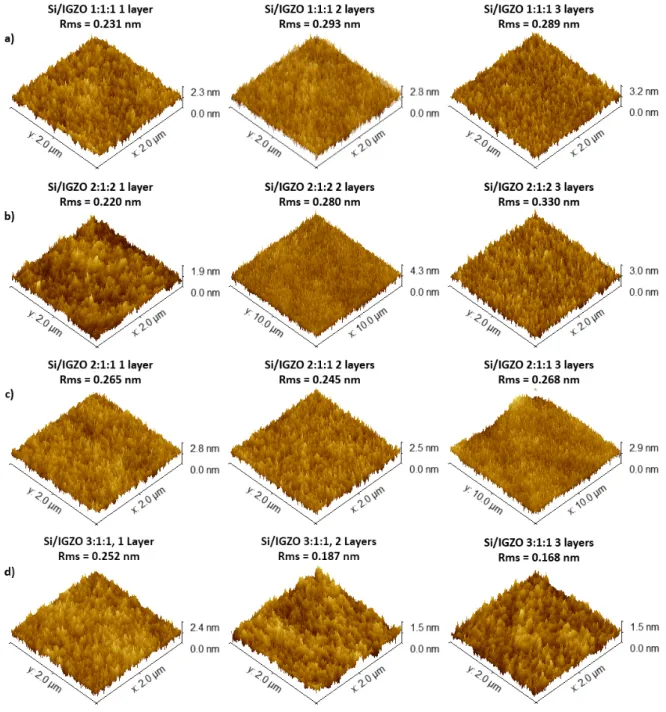
3.6 Morphological characterisation IGZO a) 1:1:1, b) 2:1:2, c) 2:1:1 and d) 3:1:1 thin films for a concentration of 0.2 M. AFM deflection images of 2×2 µm2 to an annealing at 300◦C during 30 min, with different number of IGZO layers. . . . 17
3.7 SEM surface of 3-layer IGZO 3:1:1 thin film on Si substrate, with annealing 300◦C for 30 min. . . 18
3.8 Molecular concentration (%) of each metallic oxide in IGZO thin films with 3 layers on Si substrates, annealed at 300◦C for 30 min. . . . 18
3.9 Stabilisation curves of IGZO 1:1:1, 2:1:2 and 2:1:1 0.2 M TFTs with 1, 2 and 3 active layers, without urea as fuel. . . 20
3.10 Transfer curve of IGZO 2:1:1 0.2 M TFTs with 1 active layer, without urea as fuel. 21 3.11 Transfer curve of IGZO 1:1:1 0.2 M TFT with 1 active layer, measured initially and 8 weeks later. . . 21
3.12 Transfer curves of IGZO 2:1:2 0.2 M TFTs with 1 and 2 active layers, measured initially and 8 weeks later. . . 22
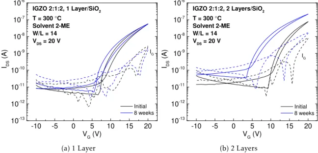
3.13 Transfer curves of IGZO 2:1:1 0.2 M TFTs with 1, 2 and 3 active layers, measured initially and 8 weeks later. . . 23
3.14 Transfer curves of IGZO 3:1:1 0.2 M TFTs with 1, 2 and 3 active layers, measured initially and 8 weeks later. . . 24
3.15 a) Transfer curves of patterned IGZO 3:1:1 3-layer IGZO; b) variation of maximum IDSwith W values studied. . . 27
C.1 DSC-TG analysis of IGZO 1:1:1 and 2:1:2 precursor solutions with 2-ME as solvent and using urea as fuel or not. . . 41
L i s t o f F i g u r e s
D.1 Reflectance spectra of IGZO thin films on glass substrates. . . 43
E.1 Tauc-bandgap plots for the calculation of Eopt. . . 46
F.1 Transconductance curve of IGZO 1:1:1 0.2 M TFT with 1 active layer, measured initially and 8 weeks later. . . 47
F.2 Transconductance curves of IGZO 2:1:2 0.2 M TFT with 1 and 2 active layers, measured initially and 8 weeks later. . . 47
F.3 Transconductance curves of IGZO 2:1:1 0.2 M TFT with 1, 2 and 3 active layers, measured initially and 8 weeks later. . . 48
F.4 Transconductance curves of IGZO 2:1:1 0.2 M TFT with 1, 2 and 3 active layers, measured initially and 8 weeks later. . . 49
F.5 Transconductance curves of TFTs annealed at 120◦C with patterned IGZO 3:1:1 3 layers, measured initially and 8 weeks later. . . 50
F.6 Transconductance curves of TFTs annealed at 180◦C with patterned IGZO 3:1:1 3 layers, measured initially and 8 weeks later. . . 51
G.1 Stabilisation curves of IGZO 1:1:1 0.2 M with 1, 2 and 3 active layers. . . 53
G.2 Stabilisation curves of IGZO 2:1:2 0.2 M with 1, 2 and 3 active layers. . . 54
G.3 Stabilisation curves of IGZO 2:1:1 0.2 M with 1, 2 and 3 active layers. . . 55
G.4 Stabilisation curves of IGZO 3:1:1 0.2 M with 1, 2 and 3 active layers. . . 56
G.5 Output curve of IGZO 1:1:1 0.2 M with 1 active layer. . . 57
G.6 Output curves of IGZO 2:1:2 0.2 M with 1 and 2 active layers. . . 57
G.7 Output curves of IGZO 2:1:1 0.2 M with 1, 2 and 3 active layers. . . 58
G.8 Output curves of IGZO 3:1:1 0.2 M with 1, 2 and 3 active layers. . . 59
H.1 Stabilisation curves of TFTs annealed at 180◦C with patterned IGZO 3:1:1 3 lay-ers, measured initially and 8 weeks later . . . 61
H.2 Saturation curves of TFTs annealed at 180◦C with patterned IGZO 3:1:1 3 layers, measured initially and 8 weeks later . . . 62
H.3 Ouput curves of TFTs annealed at 180◦C with patterned IGZO 3:1:1 3 layers, measured initially and 8 weeks later . . . 63
I.1 Stabilisation curves of IGZO 3:1:1 0.2 M with W/L of 80/20, 160/20, 320/20 µm/µm, annealed at 120◦C . . . . 65
I.2 Output characteristics of patterned IGZO 3:1:1 3 Layers, annealed at 120◦C . . 66
List of Tables
3.1 Characteristic absorbance peaks and associated vibrational modes of the
corre-sponding chemical bonds for analysed FT-IR spectra of IGZO solutions. . . 11
3.2 Thickness of measured films (nm) by spectroscopy ellipsometry, for all IGZO molar ratios, with films spin coated onto Si substrates and annealed at 300◦C. . 14
3.3 Eopt of measured films (eV) determined by linear fit of Tauc-plots, for all IGZO molar ratios, with films spin coated onto Si substrates and annealed at 300◦C. . 15
3.4 Average and standard deviation of electrical parameters of three measured TFTs with IGZO 1:1:1 1 layer as channel layer, measured initially and 8 weeks later. . 22
3.5 Average and standard deviation of electrical parameters of three measured TFTs with IGZO 2:1:2 as channel layer, measured initially and 8 weeks later. . . 22
3.6 Average and standard deviation of electrical parameters of three measured TFTs with IGZO 2:1:1 as channel layer, measured initially and 8 weeks later. . . 23
3.7 Average and standard deviation of electrical parameters of three measured TFTs with IGZO 3:1:1 as channel layer, measured initially and 8 weeks later. . . 24
3.8 Average and standard deviation of electrical parameters of three measured TFTs annealed at 120◦C with patterned-IGZO 3:1:1 as channel layer, measured initially and 8 weeks later. . . 27
A.1 Reduction and oxidation reactions. . . 37
A.2 Combination of metal nitrate reduction and fuel oxidation reactions. . . 37
A.3 Valence of the reagents. . . 38
A.4 Number of moles of fuel per mole of oxidiser to ensure stoichiometry of the redox reaction. . . 38
A.5 Overall reactions with correct stoichiometry. . . 38
B.1 Viscosities of IGZO solutions with and without urea, and 2-ME. . . 39
E.1 R2of each linear fit for determination of E opt. . . 46
H.1 Average and standard deviation of electrical parameters of three measured TFTs annealed at 180◦C with patterned-IGZO 3-layer 3:1:1 as channel layer, measured initially and 8 weeks later. . . 63
Acronyms
2-ME 2-Methoxyethahol.
a-Si Amorphous Silicon.
a-IGZO Amorphous Indium-Gallium-Zinc Oxide.
AFM Atomic Force Microscopy.
ALD Atomic Layer Deposition.
AMOLED Active-Matrix Organic Light-Emitting Diode.
ATR Atenuated Total Reflectance.
CBM Conduction Band Minimum.
CEMOP Center of Excellence in Microelectronics and Optoelectronic Processes.
CENIMAT Centro de Investigação de Materiais.
CVD Chemical Vapor Deposition.
DIW Deionised Water.
DSC Differential Scanning Calorimetry.
EDS Electron Dispersive X-Ray Spectroscopy.
FET Field Effect Transistor.
FPD Flat-Panel Display.
FSR Full Scale Range.
FT-IR Fourier Transform-Infrared Spectroscopy.
GAXRD Grazing Angle X-Ray Diffraction.
I-V Current-Voltage.
IGZO Indium-Gallium-Zinc Oxide.
IPA Isopropyl Alcohol.
IZO Indium Zinc Oxide.
AC R O N Y M S
NIR Near Infrared.
OV Oxidizing Valence.
PLD Pulsed Laser Deposition.
PR Photoresist.
Rms Root mean square.
RV Reducing Valence.
SCS Solution Combustion Synthesis.
SEM Scanning Electron Microscopy.
TAOS Transparent Amorphous Oxide Semiconductor.
TCO Transparent Conducting Oxide.
TFT Thin Film Transistor.
TG Thermogravimetry.
TSO Transparent Semiconducting Oxide.
UV Ultraviolet.
Vis Visible.
ZTO Zinc Tin Oxide.
Symbols
A Optical absorption
Ci Gate capacitance per unit area
ds Thickness
EF Fermi Level
Eopt Optical bandgap
ϕ Fuel/oxidizer ratio
gm Transconductance
h Planck constant
I Current
IDS Drain-to-source current
IG Gate leakage current
Ioff Drain current in off-state
Ion Drain current in on-state
Ion/Ioff On-offcurrent ratio
L Channel length
ν Frequency
N Carrier concentration
S Y M B O L S
R2 Coefficient of determination
SS Subthreshold Slope
T Transmittance
V Voltage
VDS Voltage between the drain and source
VGS Voltage between the gate and source
VHyst Hysteresis voltage
Von Turn-on voltage
VT Threshold voltage
µF E Field-effect mobility
µsat Saturation mobility
σ Conductivity
U Urea
W Channel width
χ2 Error function
Motivation and Objectives
Printed electronics is an expanding research area due to the potential applications in tech-nology and their impact in society. Therefore, the development of solution-based materials is crucial for electronic applications, namely transparent flexible electronics. Metal oxide-based Thin Film Transistors (TFTs) produced by solution must have good properties such as high electrical performance, reproducibility, low cost and need to be processed at low temperatures to enable their application in plastic flexible substrates.
Since it is required a semiconductor material for the active channel layer of the TFTs, the synthesis of Transparent Amorphous Oxide Semiconductors (TAOSs) is essential to the development of solution-based electronics. Amorphous Indium-Gallium-Zinc Oxide (a-IGZO) is by far the most used semiconductor for oxide-based Flat-Panel Displays (FPDs) industry, due to its high electrical performance. However, when produced by solution, its electrical properties are not yet optimised, which is the main motive to the study of solution-processed a-IGZO thin films in this work.
The main objective of this work is the study, production and optimisation of solution-based a-IGZO thin films with the benefits of Solution Combustion Synthesis (SCS), by using solutions with metallic salts for their application as active channel layer in TFTs. To achieve this, several tasks will be employed:
• Production and characterisation of solutions with different metallic cations molar
ra-tios;
C h a p t e r
1
Introduction
1.1 Metal oxide semiconductors
Over the recent years, research in electronic circuits fabricated on flexible transparent sub-strates led to the emergence of transparent flexible electronics, which is expected to meet emerging technological demands of most of microelectronics devices in the next years, in particularly displays [1, 2]. Although FPDs have been developed using Amorphous Silicon (a-Si) TFTs [3, 4], they have low field-effect mobility [1, 2, 5–7], and do not have high
trans-parency and mechanical flexibility, the fundamental pillars of emerging flexible transparent electronics [6, 8]. Organic semiconductors have been intensively studied as a-Si substitute, however they have low mobility and are less stable [1, 6, 9]; moreover, polycrystalline Si has better mobility compared to a-Si, but it has poor area uniformity due to grain boundaries and processing issues [10, 11].
Metal oxides materials have emerged as an alternative to Si technology, due to their per-formance as (semi)conductive materials, with excellent optical transparency and electrical properties [12–15]. Among devices, transparent TFTs with metal oxide semiconductors as active layer have been extensively reported over the last years, with the development and optimisation of such materials being the key to the emergence of backplane TFTs for the next generation of FPDs [16–18]. Also, TFTs can be fabricated on flexible substrates if metal oxides are used for all components, including the active, dielectric and the electrodes layers [2, 19]. Metal oxides such as ZnO, Zinc Tin Oxide (ZTO) and Indium-Gallium-Zinc Oxide (IGZO) have been reported to various applications, including Active-Matrix Organic Light-Emitting Diode (AMOLED) displays, wearable sensor arrays, flexible displays and flexible solar cells [6, 8, 20–24].
Despite crystalline oxide semiconductors have been reported, they require very high annealing temperatures, incompatible with most flexible substrates [2, 5]. TAOSs have been intensively studied and reported since Hosonoet al.proposed that oxides composed by post-transition-metal cations with an electron configuration of (n−1)d10ns0(for n≥5) create a large overlap of their spherical isotropic ns-orbitals. These are the main elements of the conduction band, forming a conduction pathway with electron mobilities > 10 cm2V−1s−1, comparable to those of the corresponding crystalline phases [2, 25–29].
C H A P T E R 1 . I N T R O D U C T I O N
1.2 Amorphous indium-gallium-zinc oxide
IGZO is by far the most studied and used TAOS in different applications, mainly as
semi-conducting n-channel layer for FPD applications, due to the high field-effect mobility, small
subthreshold slope (SS) and good uniformity. In addition, solution-processing of IGZO can be used to print TFTs, allowing to be used on flexible substrates [14, 32–36].
Structurally, a-IGZO is a multicomponent TAOS composed by three binary systems: In2O3, Ga2O3and ZnO. The In3+cations are the main constituent of the conduction band
and the only withn≥5, meaning that their ns orbitals overlap and lead to high mobilities [26]. The incorporation of Zn2+is fundamental to form stable amorphous structures, and
while Indium Zinc Oxide (IZO) films have been reported with good properties to apply as Transparent Conducting Oxide (TCO), their application as Transparent Semiconducting Oxide (TSO) is not ideal due to the difficult in decreasingN below 1017cm−3[37]. In IGZO system, Ga3+cation can form strong bonds with oxygen due to its high ionic potential and a small radius, therefore prevents excessive free carrier generation due to oxygen vacancies, although the lack of oxygen vacancies will prevent the prefilling the trapping states, reduc-ing mobility [5, 26]. Furthermore, a quaternary system composed by cations with different
sizes promotes the amorphous character and hence electrical uniformity, smooth surfaces and flexibility due to the lack of grain boundaries. [6, 27]. Given this, the electrical prop-erties of a-IGZO can be easily tuned for specific functions by varying cations proportions, therefore an understanding of composition influence on electrical performance is crucial for developing a-IGZO-based TFTs [38].
1.3 Solution-based electronics
There are many deposition methods for metal oxide films; most of them are vacuum-based techniques, such as Atomic Layer Deposition (ALD), Chemical Vapor Deposition (CVD), Pulsed Laser Deposition (PLD) and radio frequency sputtering [2, 39–43]. Although they have been the most used and allow high-quality devices to be produced with reasonable performance and reliability, the high costs, temperature processing, need of vacuum sources and slow processing time are the major problems of these techniques [8, 44–46]. Therefore, solution-processing of metal oxides has become an attractive alternative due to the low-cost, high-throughput, roll-to-roll processing scalability and compositional control. Solution processes have lower equipment costs compared with vacuum-based processes [16, 46–48]. Typical solution deposition methods are spin-coating, spray pyrolysis, dip-coating, inkjet printing, and chemical bath deposition [49–53].
Research on solution-TAOSs has recently earned a lot of attention in large-scale fabrica-tion of large-area electronics, because they are easily processed and have high transparency, opening new horizons for low-cost printable and transparent electronics on flexible sub-strates [9, 32]. Excellent films with ZnO, ZTO, IZO and IGZO grown by solution processes have been reported for the application of FPDs [13, 24, 30, 53] .
1 . 4 . S O LU T I O N C O M B U S T I O N S Y N T H E S I S
1.4 Solution combustion synthesis
One of the major drawbacks concerning solution-based routes for metal oxides is the need of an annealing step at relatively high temperatures to promote condensation and densification by the degradation of impurities, which adversely affect the device performance [25, 33, 48].
High annealing temperatures restrict the compatibility of TFTs with flexible substrates used in transparent flexible electronics [32, 44, 54, 55].
Given the emergence of flexible electronics, a general approach to low temperature solu-tion processing of metal oxide films called SCS has been developed in the last years [8, 22, 56, 57]. In this method, the introduction of an oxidising agent (in the form of a metal nitrate salt) and a fuel as reducing agent (typically urea) into the precursor solution leads to the enhance-ment of the oxide precursor potential (Figure 1.1a). When the solution is spin-coated and annealed, a local highly exothermic chemical reaction occurs within the film, which leads to the formation of Metal-Oxide-Metal (M-O-M) lattice and a rapid efficient condensation.
The required processing temperature (usually 250-300 ◦C) acts only as exothermic redox reaction initiator rather than a temperature that must be applied to achieve and to maintain decomposition and phase formation (Figure 1.1b) [58–60].
Figure 1.1: a) Schematic reaction coordinate comparing the energetics for SCS and conven-tional sol-gel solution processing; b) comparison of SCS and convenconven-tional reactions to form metal oxides. Adapted from [8].
1.5 Thin film transistors
TFTs are the fundamental building blocks of thin film electronics, because they are mostly used as on-offswitches of the pixels in FPDs. They are the key devices for the application of
TAOSs in transparent electronics.
A TFT is a Field Effect Transistor (FET) comprising three electrodes (gate, source and
drain), a semiconductor placed between the source and drain electrodes, and an insulator (or dielectric) material inserted between the semiconductor and the gate electrode. By applying an electric field between source and drain electrodes, a current (IDS) may flow between these
electrodes, being modulated by a voltage applied in the gate electrode, which allows to turn on or off the device, acting as a switch. The semiconductor layer allows the formation of
C H A P T E R 1 . I N T R O D U C T I O N
two structures: in a coplanar structure, the electrodes are all on the same side, while in a staggered structure the gate is opposite to the side of drain and source electrodes. For each structure, two configurations are possible: top-gate (or normal) or bottom-gate (or inverted), depending on whether if the gate electrode is on top or bottom of the structure [62].
Figure 1.2: Structure of a staggered bottom-gate TFT.
Considering n-type TFTs, they can be classified as enhancement or depletion-mode, whether if the threshold voltage (VT) is positive or negative. When VGS>VT, for a given
applied positive VDS a significant density of electrons is accumulated in
semiconductor/di-electric interface, enough to have a current IDS flowing between drain and source, which
corresponds to the on-state of the TFT. In contrast, for VGS<VT, the device is off-state, for
any given VDSapplied. There are two different operation regimes in the on-state, depending
of VDSvalue: linear and saturation regimes. The first one is described by Equation 1.1, when
VDS< VGS−VT[62]:
IDS=WL CiµFE
(VGS−VT)VDS−
1 2V
2
DS
(1.1)
where W and L are the channel width and length, respectively. Ci is the gate capacity
per unit area andµFE is the field-effect mobility. When VDS≪VGS-VT, by neglecting the
quadratic term, a linear relation between IDSand VDSis obtained, maintaining an uniform
channel charge density across the channel from source to drain.
The saturation regime is described by Equation 1.2, when VDS> VGS−VT:
IDS=2WLCiµsat(VGS−VT)2 (1.2)
whereµsat is the saturation mobility. In this regime, the region near the drain is com-pletely depleted (pinch-offeffect), leading to a constant and saturated IDS[62].
By analysing the transfer and output curves of TFTs, the static characteristics can be obtained, depicted in Figure 1.3. Quantitative parameters such as mobility, on-off ratio
current (Ion/Ioff), VTand turn-on voltage (Von) can be extracted by the transfer characteristics
(Figure 1.3a) [37, 62].
The mobility is the facility that carriers have to move through the material [5]; in the linear region the mobility is defined asµFE and is given by Equation 1.3:
1 . 5 . T H I N F I L M T R A N S I S T O R S
µFE=
∂√ID
∂VGS
W LCiVDS
(1.3)
For saturation regime mobility is defined as saturation mobility (µsat), given by Equation 1.4:
µsat=
∂√ID
∂VGS
2
1 2CiWL
(1.4)
TheSSis the minimum VGSto increase IDSby one decade, and is obtained by Equation
1.5:
SS=
dlogIDS
dVGS
max
−1
(1.5)
The Ion/Ioffis given by the ratio of the maximum and minimum IDS; for typical electronic
applications, it is usually required values above 106. V
T can be determined by different
methodologies, such as linear extrapolation of√IDS-VGSplot for high VDS; it gives the VGS
value at which the conductive channel is formed close to the semiconductor/dielectric inter-face. Voncorresponds to the VGS value at which IDS starts to increase. Output curves are
plotted for different VGS values, allowing to distinguish linear and saturation regimes, in
function of VDSfor a fixed VGS(Figure 1.3b) [37].
(a) Transfer (b) Output
C h a p t e r
2
Materials and Methods
This section summarises the main procedures and techniques used during this work, con-cerning the production of IGZO solutions, as well as their characterisation, and fabrication and electrical characterisation of IGZO TFTs.
IGZO TFTs were studied by varying the molar ratio of metallic cations and the number of active layers, to determine the best condition to apply as TFT channel. Finally, TFTs with the best performing conditions were produced and patterned.
2.1 Precursor solutions preparation and characterisation
The metallic oxide precursor solutions were prepared by dissolving individually indium (III) nitrate hydrate (In(NO3)3·xH2O, Sigma, 99.9%), gallium (III) nitrate hydrate (Ga(NO3)3·xH2O,
Sigma, 99.9%) and zinc nitrate hexahydrate (Zn(NO3)2·6H2O, ACROS Organics, 98%) in
2-Methoxyethahol (2-ME) (C3H8O2, ACROS Organics, >99.5%), to yield solutions with a
concentration of 0.2 M. For the combustion reaction, urea (CO(NH2)2, Sigma, 98%) was
added as fuel to each precursor solution, with molar ratios between urea and indium nitrate, gallium nitrate, and zinc nitrate of 2.5:1, 2.5:1 and 1.67:1 respectively, to guarantee the redox stoichiometry of the reaction (see Appendix A). All precursor solutions were magnetically stirred at 430 rpm for 1 h at room temperature in air environment.
The IGZO semiconductor precursor solutions were prepared by mixing indium nitrate, gallium nitrate and zinc nitrate precursor solutions to obtain In2O3:Ga2O3:ZnO molar ratios
of of 1:1:1, 2:1:1, 2:1:2 and 3:1:1, all with a 0.2 M concentration. IGZO solutions were magnetically stirred at 430 rpm for at least 24 h at room temperature in air environment. All IGZO precursor solutions were filtrated through 0.2 µm hydrophilic filters.
Thermal and chemical characterisation of precursor solutions were performed by Diff
C H A P T E R 2 . M AT E R I A L S A N D M E T H O D S
2.2 Thin films deposition and characterisation
Prior to deposition all substrates (p+Si with a 100 nm thermally grown SiO2layer, Si wafer
and soda-lime glass, each one with an area of 2.5x2.5 cm2) were cleaned in an ultrasonic bath
at 60◦C in acetone for 15 min, then in Isopropyl Alcohol (IPA) for 15 min. Subsequently, the substrates were cleaned with Deionised Water (DIW) and dried under N2, followed by a
15 min Ultraviolet (UV)/Ozone surface activation step for a distance lamp of 7 cm using a PSD-UV Novascan system.
To study the effect of the number of active layers, IGZO thin films were deposited onto
SiO2 substrates by sequentially spin coating 1 to 3 layers of IGZO precursor solution for
35 s at 3000 rpm (Laurell Technologies), followed by an immediate hot plate annealing at 300◦C for 30 min after each layer, in ambient conditions, to ensure the exothermic reaction. The structure of the films was assessed by Grazing Angle X-Ray Diffraction (GAXRD) ,
using a X’Pert PRO PANalytical diffractometer with Cu Kα line radiation (λ= 1.540598
Å) and an angle of incidence of the X-ray beam fixed at 0.75◦, in the range of 20◦ to 50◦ (2θ). The films’ surface morphology was studied by Scanning Electron Microscopy (SEM) Zeiss Auriga Crossbeam electron microscope and Atomic Force Microscopy (AFM) Asylum MFP3D. Electron Dispersive X-Ray Spectroscopy (EDS) was performed to study the chemical composition of the thin films. Spectroscopic ellipsometry was used to measure the thin films thickness deposited on Si substrates, with an energy range from 1.5 to 5.5 eV and an incident angle of 45◦ using a Jobin Yvon Uvisel system. The acquired data were modulated using the DELTAPSI software, and the fitting procedure was done pursuing the minimisation of the error function (χ2). FT-IR spectroscopy characterisation of thin films deposited in Si substrates was performed the same way as used for IGZO precursor solutions. The optical properties were obtained by a Perkin Elmer lambda 950 UV/Visible (Vis)/Near Infrared (NIR) spectrophotometer. The transmittance (T) and reflectance (R) were obtained in a wavelength range from 200 to 2500 nm.
2.3 Electronic devices fabrication and characterisation
Non-patterned TFTs were produced in a staggered bottom-gate, top-contact structure by spin coating IGZO thin films (see section 2.2) onto 100-nm-thick SiO2 thermally oxidised
on p+Si wafer (C
i= 35×10−9F/m2). Aluminium source and drain electrodes (80 nm thick) were deposited on IGZO films via a shadow mask by thermal evaporation. The channel length and width of the IGZO TFTs were 1400 µm and 100 µm, respectively (W/L=14). A post-annealing step was performed on a hot plate for 1 h at 120◦C in air environment.
Regarding the semiconductor patterning of TFTs, positive Photoresist (PR) AZ ECL 3012 was spin-coated onto the IGZO thin films (Headway Research PWM32), firstly at 3000 rpm for 10 s and then at 4000 rpm for 20 s. After that, substrates were soft-baked in a hot-plate at 115◦C for 1 min and 15 s. Lithography mask with semiconductor patterns was aligned with the substrate in a mask aligner (Karl-Suss MA6); then, UV exposure in soft-contact mode was proceeded for 2.5 s. Substrates were dipped in a developer solution (AZ 726 MIF) to
2 . 3 . E L E C T R O N I C D E V I C E S FA B R I CAT I O N A N D C H A R AC T E R I SAT I O N
obtain the PR pattern, and immersed in etching solution (HCl·H2O 20:1) for 20 s to etch
IGZO with the desired pattern, then dipped sequentially in acetone and DIW to remove the remaining PR and water to clean the sample. The final step comprised the aluminium contacts patterning: first PR was spin-coated and soft-baked with the same conditions as for IGZO, followed by alignment of a negative mask containing source-drain electrodes patterns with the existing IGZO ones to UV exposure. Substrates were dipped in developer and aluminium was deposited via thermal evaporation. Finally, the aluminium in excess was removed by dipping the substrates in acetone to remove PR and all aluminium above PR (lift-off). A post-annealing step was performed on a hot plate for 1 h at 120◦C in air environment.
C h a p t e r
3
Results and Discussion
This chapter discusses the results regarding the characterisation of solutions, thin films and the electrical characterisations of the produced TFTs.
3.1 Solutions characterisation
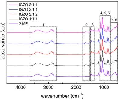
Analysis of elements through characteristic spectra of IGZO thin films using urea as fuel was performed by FT-IR, using ATR, and data presented in wavenumber range of 4000-525 cm−1. Figure 3.1 depicts the FT-IR spectra of IGZO solutions for each molar ratio studied. Correction of the atmospheric contribution was performed for all spectra. Most of the peaks are related with organic compounds present in 2-ME, identified in Table 3.1. [63, 64].
4000 3000 2000 1000
7, 8 4, 5, 6
3 3
1 2
IGZO 3:1:1 IGZO 2:1:1 IGZO 2:1:2 IGZO 1:1:1 2-ME
a
b
s
o
rv
a
n
c
e
(
a
.u
)
wavenumber (cm-1)
Figure 3.1: FT-IR spectra of IGZO solutions, with different molar ratios.
Table 3.1: Characteristic absorbance peaks and associated vibrational modes of the corre-sponding chemical bonds for analysed FT-IR spectra of IGZO solutions.
Number Position (cm−1) Mode type Chemical bond
1 3500 Stretching vibration M-OH
2, 5 1620, 1015 Bending vibration M-OH
3 1388 Stretching vibration NO3–
4 1107 Transversal optic stretching Si-O
6 833 Bending vibration NO3–
C H A P T E R 3 . R E S U LT S A N D D I S C U S S I O N
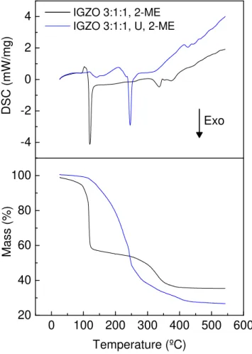
3.1.1 Thermal characterisation
Thermal characterisation was performed to evaluate the decomposition of metal oxides. IGZO 0.2 M solutions were analysed, with and without urea for further comparison. Figure 3.2 depicts the DSC-TG results for IGZO 3:1:1 with and without urea in 2-ME. DSC and TG results for IGZO 1:1:1, 2:1:2 and 2:1:2 are represented in Appendix C.
0 100 200 300 400 500 600 20
40 60 80 100 -4 -2 0 2 4
M
a
s
s
(
%
)
Temperature (ºC)
IGZO 3:1:1, 2-ME IGZO 3:1:1, U, 2-ME
D
S
C
(
m
W
/m
g
)
Exo
Figure 3.2: DSC-TG analysis of IGZO 3:1:1 precursor solutions with 2-ME as solvent and using urea as fuel or not.
Regarding IGZO solution with urea, two endothermic peaks are present (at 112◦C and 211◦C) accompanied by a mass loss, related with evaporation of solvent and water. Then there is an intense exothermic peak (at 245◦C) accompanied by a large mass loss, corre-sponding to the redox reaction of the formation of oxides. A smaller endothermic peak at 426◦C is related with degradation of residual organics.
Concerning IGZO solution without urea, it is visible a small endothermic peak around 100◦C, which is related with water and solvent evaporation events [59]. Then, there is an intense exothermic peak at 121◦C accompanied by an abrupt mass loss, corresponding to the formation of oxides. Comparing with the solution without urea, the exothermic peak at lower temperature can be justified by the solvent 2-ME acting as fuel itself to initiate the redox reaction. According to Salgueiroet al. the organic solvent possesses a reducing nature, then it can also act as fuel, leading to a combustion reaction [59]. The exothermic
3 . 2 . T H I N F I L M S C H A R AC T E R I SAT I O N
peak of IGZO with urea is more intense, since the addition of urea increases the organic content in the solution, therefore additional energy is required to ensure the combustion. Also, the exothermic peak at 335◦C is associated with residual organics, meaning that the degradation of organics requires at least two phases without use of urea. Nevertheless, the exothermic peak of IGZO with urea occurs at a temperature below 300◦C, meaning that the annealing temperature used during the production of thin films is enough to promote the redox reaction.
It is important to mention that process parameters can strongly influence the DSC-TG measurements, namely the heating rate and the evaporation solvent step previous to DSC-TG analysis. In the case of solutions with urea, during the evaporation of solvent some urea could initiate combustion reaction prior to the DSC-TG analysis, leading to a non-stoichiometric condition during DSC-TG measurements, with the fuel/oxidiser ratio (ϕ) < 1 (see Appendix A). This leads to the formation of more organic compounds as products of the reaction.
3.2 Thin films characterisation
FT-IR spectra of 3-layer IGZO thin films spin coated on Si substrates after being annealed at 300◦C for 30 min were obtained, with correction of the atmospheric contribution performed for all spectra (Figure 3.3).
1100 1000 900 800 700 600 500
7 IGZO 3 Layers 0.2 M
T = 300 °C, 30 min
Solvent 2-ME, Si
4
8
3:1:1 2:1:1 2:1:2 1:1:1
a
b
s
o
rb
a
n
c
e
(
a
.u
.)
wavenumber (cm-1)
Figure 3.3: FT-IR spectra of 3-layer IGZO thin films on Si substrates, with different molar
ratios, after annealing at 300◦C for 30 min.
C H A P T E R 3 . R E S U LT S A N D D I S C U S S I O N
the presence of M-O bonds in thin films after annealing. Note that FT-IR spectra above 1150 cm−1is not shown in Figure 3.3 because no peaks were observed.
3.2.1 Optical characterisation
Spectroscopic ellipsometry was used to measure the thickness of all thin films. The measured thickness values are shown on table 3.2, for each number of IGZO layers and molar ratios.
Table 3.2: Thickness of measured films (nm) by spectroscopy ellipsometry, for all IGZO molar ratios, with films spin coated onto Si substrates and annealed at 300◦C.
Number of Layers IGZO molar ratio
1:1:1 2:1:2 2:1:1 3:1:1
1 13.6±0.1 14.2±0.1 13.7±0.1 14.2±0.1 2 28.1±0.2 27.4±0.3 24.0±0.6 26.6±0.2 3 38.8±0.1 38.2±0.3 36.2±0.3 35.9±0.4
For a fixed number of spin coated layers, the values are similar, regardless the molar ratios.
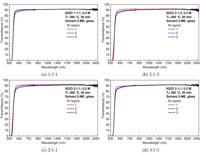
Both transmittance and reflectance of IGZO thin films on soda-lima glass substrates were measured, in a wavelength range of 200-2500 nm with a step of 3 nm. Figure 3.4 depicts transmittance spectra for IGZO thin films. The values of transmittance are around 90% in almost entire wavelength range. The increasing number of deposited layers affects the
transmittance in the visible region due to the increase of the thickness; despite this, values between 85-90% are obtained for all conditions [65]. Reflectance spectra of IGZO thin films are represented in Appendix D.
3 . 2 . T H I N F I L M S C H A R AC T E R I SAT I O N
200 450 700 950 1200 1450 1700 1950 2200 2450 0 10 20 30 40 50 60 70 80 90 100 T ra n s m it ta n c e ( % ) Wavelength (nm) Nr layers 1 2 3 IGZO 1:1:1, 0.2 M T= 300 °C, 30 min Solvent 2-ME, glass
(a) 1:1:1
200 450 700 950 1200 1450 1700 1950 2200 2450 0 10 20 30 40 50 60 70 80 90 100 T ra n s m it ta n c e ( % ) Wavelength (nm) Nr layers 1 2 3 IGZO 2:1:2, 0.2 M T= 300 °C, 30 min Solvent 2-ME, glass
(b) 2:1:2
200 450 700 950 1200 1450 1700 1950 2200 2450 0 10 20 30 40 50 60 70 80 90 100 T ra n s m it ta n c e ( % ) Wavelength (nm) Nr layers 1 2 3 IGZO 2:1:1, 0.2 M T= 300 °C, 30 min Solvent 2-ME, glass
(c) 2:1:1
200 450 700 950 1200 1450 1700 1950 2200 2450 0 10 20 30 40 50 60 70 80 90 100 T ra n s m it ta n c e ( % ) Wavelength (nm) Nr layers 1 2 3 IGZO 3:1:1, 0.2 M T= 300 °C, 30 min Solvent 2-ME, glass
(d) 3:1:1
Figure 3.4: Transmittance spectra of IGZO thin films on glass substrates.
Eoptvalues were obtained by Tauc-bandgap plots; the values are represented in table 3.3,
and the calculation steps are explained in Appendix E.
Table 3.3: Eopt of measured films (eV) determined by linear fit of Tauc-plots, for all IGZO
molar ratios, with films spin coated onto Si substrates and annealed at 300◦C.
Number of Layers IGZO molar ratio 1:1:1 2:1:2 2:1:1 3:1:1
1 3.73 3.75 3.71 3.72
2 3.74 3.73 3.74 3.73
3 3.72 3.74 3.68 3.72
In multicomponent oxides, Eopt is affected by atomic composition of each cation, and
values are generally closer to the Eopt of the dominant cations. Therefore, In IGZO 2:1:1
and 3:1:1 (4:2:1 and 6:2:1 in atomic ratio, respectively), it is expected to obtain an Eopt
similar to the obtained in literature by In2O3 (about 3.5-3.7 eV). In IGZO 1:1:1 (2:2:1 in
atomic ratio), the Ga2O3content leads to higher Eoptvalues because it has a Eoptaround 4.16
eV; therefore obtained values were intermediate to Eopt of In2O3 and Ga2O3, as expected.
Finally, IGZO 2:1:2 (4:2:2) ZnO should contribute to a decrease in Eopt due to its lower
reported Eopt (3.24 eV). Despite this, all obtained values are in a range of 3.68-3.75 eV,
C H A P T E R 3 . R E S U LT S A N D D I S C U S S I O N
of defects due to a high porous structure in all thin films, combined with small thickness values. Nevertheless, all values are above 3 eV, meaning that all films produced meet the required criteria for optical transparent applications [37].
3.2.2 Structural and morphological characterisation
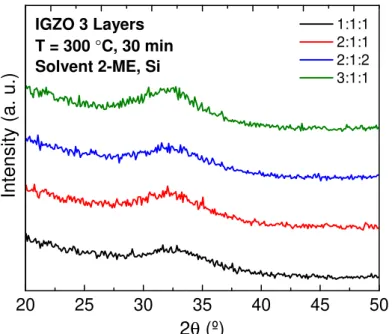
To evaluate the amorphous character of the thin films structure, GAXRD measurements were performed on 3-layer IGZO thin films annealed at 300◦C. GAXRD diffractograms of thin
films with IGZO molar ratios of 1:1:1, 2:1:1, 2:1:2 and 3:1:1 are shown in Figure 3.5.
1:1:1 2:1:1 2:1:2 3:1:1
20 25 30 35 40 45 50
IGZO 3 Layers
T = 300 °C, 30 min
Solvent 2-ME, Si
In
te
n
s
it
y
(
a
.
u
.)
2
θ
(º)
Figure 3.5: GAXRD diffractograms of 3-layer IGZO thin films on Si substrates, with different
molar ratios.
GAXRD diffractograms have shown that thin films are amorphous independently the
IGZO molar ratio, exhibiting only a broad peak centred at 2θ= 32-34◦in all samples, typical of amorphous binary and multicomponent oxide films composed by indium, gallium and/or zinc [37, 66, 67]. Since IGZO is a quaternary multicomponent oxide composed by three dif-ferent metallic cations, the degree of disorder of the structure is higher than binary/ternary oxides as aforementioned before in section 1.2, therefore IGZO it is harder to crystallise at this temperature.
The surface topography of IGZO thin films spin coated on Si substrates was measured using AFM. Surface roughness was obtained by measuring Root mean square (Rms) in alter-nate mode and the topographic images were analysed in data analysis software Gwyddion. Surface topographies of all thin films are presented in Figure 3.6. The surface roughness of the films was determined from the AFM height profile of a 2×2µm2area scan. Acquired AFM images for films revealed a very smooth and homogeneous surface, with Rms close to 0.2 nm in all cases, typical for reported combustion-processed amorphous semiconductors [6, 25].
3 . 2 . T H I N F I L M S C H A R AC T E R I SAT I O N
Figure 3.6: Morphological characterisation IGZO a) 1:1:1, b) 2:1:2, c) 2:1:1 and d) 3:1:1 thin films for a concentration of 0.2 M. AFM deflection images of 2×2µm2 to an annealing at 300◦C during 30 min, with different number of IGZO layers.
C H A P T E R 3 . R E S U LT S A N D D I S C U S S I O N
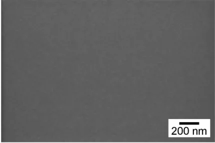
Figure 3.7: SEM surface of 3-layer IGZO 3:1:1 thin film on Si substrate, with annealing 300◦C for 30 min.
Despite the resolution of the image, crystalline structures are not visible, giving support to GAXRD results regarding the amorphous character of the thin films.
Figure 3.8 shows the obtained molecular concentration of each metallic oxide, for each studied IGZO molar ratio. EDS analysis results have shown that most of the molecular compositions are closer to the expected; some discrepancies, especially regarding In content in IGZO 1:1:1, can be related to non-uniformity of the scanned area during EDS analysis.
1:1:1 2:1:2 2:1:1 3:1:1
0 10 20 30 40 50 60
M
o
la
r
p
e
rc
e
n
ta
g
e
(
%
)
In2O3:Ga2O3:ZnO
In Ga Zn
Figure 3.8: Molecular concentration (%) of each metallic oxide in IGZO thin films with 3 layers on Si substrates, annealed at 300◦C for 30 min.
3 . 3 . E L E C T R I CA L C H A R AC T E R I SAT I O N O F S O LU T I O N - BA S E D I G Z O T F T S
3.3 Electrical characterisation of solution-based IGZO TFTs
The main focus of this work is the study of solution-processed IGZO applied as channel layer on TFTs, therefore electrical characterisation of these devices is crucial, by measuring the Current-Voltage (I-V) curves, which allow to determine their important electric parameters, as well evaluate the current behaviour in function of the voltage applied.
For all devices, four consecutive stabilisation characteristics were measured (one single and three appends), with VGSranging from -10 to 20 V and VDSvalues being 20 and 10 V
for non-patterned and patterned devices, respectively. Then, transfer curves were performed in double sweep mode and used to extract Von, VT,VHyst,SS,µsat and Ion/Ioff, with the same
values of VGS range and VDS. Output characteristics were measured with VDS values
de-scribed before and 8 steps of VGS, from 0 to 20 V. The transconductance (gm) variation with
VGS-VT was obtained for each condition, being the plots depicted in Appendix F.
Electri-cal parameters were extracted for the best three performing devices and their average and standard deviation were calculated.
All non-patterned devices studied have a W/L of 1400 µm/100µm, while patterned devices were studied with W/L values of 80/20, 160/20 and 320/20µm/µm.
Ageing effects are also presented in this section, being depicted in the I-V curves
mea-sured when devices were fabricated and 8 weeks later.
In this work four different IGZO molar ratios were studied: 1:1:1, 2:1:2, 2:1:1 and 3:1:1.
These proportions were chosen in order to evaluate the influence of each cation composition in TFT performance. IGZO 1:1:1 has the same percentage of each oxide molecules, while IGZO 2:1:2 has more indium and zinc than IGZO 1:1:1. IGZO 2:1:1 has indium as dominant cation, and as it will be seen later, this is a crucial condition to obtain TFTs with desired behaviour and electrical parameters; for this reason, IGZO 3:1:1 using urea was also studied.
C H A P T E R 3 . R E S U LT S A N D D I S C U S S I O N
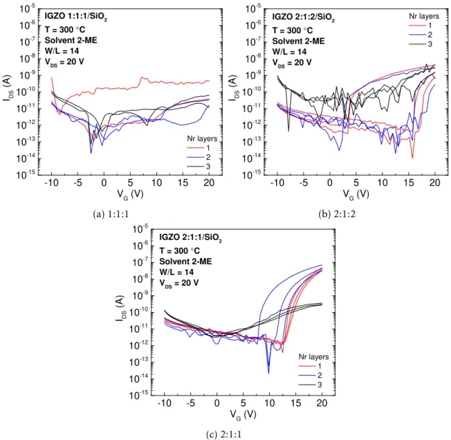
-10 -5 0 5 10 15 20
10-15 10-14 10-13 10-12 10-11 10-10 10-9 10-8 10-7 10-6 10-5 Nr layers 1 2 3 IGZO 1:1:1/SiO2
T = 300 °C Solvent 2-ME W/L = 14 VDS = 20 V
IDS
(
A
)
VG (V)
(a) 1:1:1
-10 -5 0 5 10 15 20
10-15 10-14 10-13 10-12 10-11 10-10 10-9 10-8 10-7 10-6 10-5 Nr layers 1 2 3 IGZO 2:1:2/SiO2
T = 300 °C Solvent 2-ME W/L = 14 VDS = 20 V
IDS
(
A
)
VG (V)
(b) 2:1:2
-10 -5 0 5 10 15 20
10-15 10-14 10-13 10-12 10-11 10-10 10-9 10-8 10-7 10-6 10-5 Nr layers 1 2 3 IGZO 2:1:1/SiO2
T = 300 °C Solvent 2-ME W/L = 14 VDS = 20 V
IDS
(
A
)
VG (V)
(c) 2:1:1
Figure 3.9: Stabilisation curves of IGZO 1:1:1, 2:1:2 and 2:1:1 0.2 M TFTs with 1, 2 and 3 active layers, without urea as fuel.
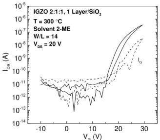
Most of the devices studied present high instability; TFTs with IGZO 2:1:1 1 layer have shown better stability and their electrical parameters were extracted from transfer curve present in Figure 3.10. The device has an Ion/Ioff of 6.4×10⁴, Von, VT and Vhyst of 14.29,
18.81 and 1.8, respectively, an SS of 0.92 V/dec and µsat of 0.01 cm2V−1s−1. In all cases, instability can be attributed to incomplete formation of M-O-M lattice during annealing. Using urea as fuel might ignite a more intense exothermic reaction, releasing more local energy to fully convert metal hydroxides into M-O-M lattice, with less residual organics, as it was observed in thermal characterisation of precursor solutions. Besides this, it can be observed an increasing degree of instability with higher number of layers. This can be related with increasing number of interfaces between deposited semiconducting layers, where electron traps can be incorporated, consequently degrading severely stabilisation and electric parameters.
3 . 3 . E L E C T R I CA L C H A R AC T E R I SAT I O N O F S O LU T I O N - BA S E D I G Z O T F T S
Concerning the metallic cations composition, IGZO 2:1:1 has shown better stabilisation characteristics probably because, as it will be seen later in IGZO TFTs produced with urea as fuel, the presence of indium as dominant cation is crucial to obtain better stability and electrical parameters.
-10 0 10 20 30
10-14 10-13 10-12 10-11 10-10 10-9 10-8 10-7 10-6 10-5
IGZO 2:1:1, 1 Layer/SiO2 T = 300 °C
Solvent 2-ME W/L = 14 VDS = 20 V
IDS
(
A
)
VG (V)
IG
Figure 3.10: Transfer curve of IGZO 2:1:1 0.2 M TFTs with 1 active layer, without urea as fuel.
TFTs with IGZO 1:1:1 molar ratio using urea as fuel were studied. Figure 3.11 depicts the transfer curve of a TFT with 1 IGZO 1:1:1 active layer, and extracted electrical parameters of three devices are shown in Table 3.4. TFTs with 2 and 3 IGZO 1:1:1 active layers have shown high instability (see Appendix G).
-10 -5 0 5 10 15 20
10-14 10-13 10-12 10-11 10-10 10-9 10-8 10-7
Initial 8 weeks IG IGZO 1:1:1, 1 Layer/SiO2
T = 300 °C Solvent 2-ME W/L = 14 VDS = 20 V
IDS
(
A
)
VG (V)
C H A P T E R 3 . R E S U LT S A N D D I S C U S S I O N
Table 3.4: Average and standard deviation of electrical parameters of three measured TFTs with IGZO 1:1:1 1 layer as channel layer, measured initially and 8 weeks later.
Layers Age Ion/Ioff Von(V) VT(V) VHyst(V) SS (V/dec) µsat(cm2V−1s−1)
1 Initial (4.26±1.52)×104 4.46±1.15 7.52±0.37 1.68±0.12 0.91±0.38 (9.00±0.82)×10−4
8 weeks (2.43±0.44)×104 3.93±1.16 6.67±0.61 1.52±0.09 0.71±0.07 (7.30±1.20)×10−4
Figure 3.12 depicts the transfer curves of TFTs with 1 and 2 IGZO 2:1:2 active layers; IGZO 2:1:2 TFTs with 3 layers have shown high instability, as shown in Figure G.2 in Ap-pendix G. Extracted electrical parameters of three devices are shown in Table 3.5.
-10 -5 0 5 10 15 20
10-13 10-12 10-11 10-10 10-9 10-8 10-7 10-6 IG Initial 8 weeks IGZO 2:1:2, 1 Layer/SiO2
T = 300 °C Solvent 2-ME W/L = 14 VDS = 20 V
IDS
(
A
)
VG (V)
(a) 1 Layer
-10 -5 0 5 10 15 20
10-13 10-12 10-11 10-10 10-9 10-8 10-7 10-6 IG Initial 8 weeks IGZO 2:1:2, 2 Layers/SiO2
T = 300 °C Solvent 2-ME W/L = 14 VDS = 20 V
IDS
(
A
)
VG (V)
(b) 2 Layers
Figure 3.12: Transfer curves of IGZO 2:1:2 0.2 M TFTs with 1 and 2 active layers, measured initially and 8 weeks later.
Table 3.5: Average and standard deviation of electrical parameters of three measured TFTs with IGZO 2:1:2 as channel layer, measured initially and 8 weeks later.
Layers Age Ion/Ioff Von(V) VT(V) VHyst(V) SS (V/dec) µsat(cm2V−1s−1)
1 Initial (1.35±0.72)×104 6.07±1.00 9.10±0.81 1.09±0.35 1.11±0.31 (3.00±0.70)×10−3
8 weeks (7.82±3.49)×103 6.25±0.50 9.23±0.43 1.33±0.16 0.97±0.19 (2.33±0.47)×10−3
2 Initial (1.02±0.42)×104 7.68±2.21 9.63±1.77 1.15±0.23 0.88±0.09 (6.00±0.14)×10−3
8 weeks (9.13±3.88)×103 4.46±1.52 7.46±0.79 1.09±0.16 1.17±0.25 (5.53±0.18)×10−3
Transfer curves of TFTs with 1, 2 and 3 IGZO 2:1:1 layers are shown in Figure 3.13. Statistic parameters of the three best devices are represented in Table 3.6.
3 . 3 . E L E C T R I CA L C H A R AC T E R I SAT I O N O F S O LU T I O N - BA S E D I G Z O T F T S
-10 -5 0 5 10 15 20
10-13 10-12 10-11 10-10 10-9 10-8 10-7 10-6 10-5 IG Initial 8 weeks IGZO 2:1:1, 1 Layer/SiO2
T = 300 °C Solvent 2-ME W/L = 14 VDS = 20 V
IDS
(
A
)
VG (V)
(a) 1 Layer
-10 -5 0 5 10 15 20
10-13 10-12 10-11 10-10 10-9 10-8 10-7 10-6 10-5 IG Initial 8 weeks IGZO 2:1:1, 2 Layers/SiO2
T = 300 °C Solvent 2-ME W/L = 14 VDS = 20 V
IDS
(
A
)
VG (V)
(b) 2 Layers
-10 -5 0 5 10 15 20
10-13 10-12 10-11 10-10 10-9 10-8 10-7 10-6 10-5 IG Initial 8 weeks IGZO 2:1:1, 3 Layers/SiO2
T = 300 °C Solvent 2-ME W/L = 14 VDS = 20 V
IDS
(
A
)
VG (V)
(c) 3 Layers
Figure 3.13: Transfer curves of IGZO 2:1:1 0.2 M TFTs with 1, 2 and 3 active layers, measured initially and 8 weeks later.
Table 3.6: Average and standard deviation of electrical parameters of three measured TFTs with IGZO 2:1:1 as channel layer, measured initially and 8 weeks later.
Layers Age Ion/Ioff Von(V) VT(V) VHyst(V) SS (V/dec) µsat(cm2V−1s−1)
1 Initial (1.48±0.75)×105 6.07±0.44 8.14±0.51 0.75±0.09 0.61±0.05 (1.00±0.03)×10−2
8 weeks (4.18±0.47)×105 3.61±0.23 6.96±0.16 0.74±0.27 0.47±0.05 (7.33±0.1)×10−3
2 Initial (1.50±0.50)×104 4.46±0.75 6.33±0.70 0.47±0.06 0.86±0.27 (2.33±0.47)×10−2
8 weeks (5.08±2.34)×103 0.01±0.67 4.42±0.42 0.74±0.07 2.01±0.26 (2.33±0.47)×10−2
3 Initial (4.54±2.86)×104 4.00±1.41 5.99±1.40 0.80±0.11 0.95±0.20 (2.30±0.47)×10−2
8 weeks (1.02±0.41)×104 0.71±0.44 2.96±0.38 0.45±0.02 1.24±0.13 (2.00±0.03)×10−2
C H A P T E R 3 . R E S U LT S A N D D I S C U S S I O N
-10 -5 0 5 10 15 20
10-13 10-12 10-11 10-10 10-9 10-8 10-7 10-6 10-5 Initial 8 weeks IG IGZO 3:1:1, 1 Layer/SiO2
T = 300 °C Solvent 2-ME W/L = 14 VDS = 20 V
IDS
(
A
)
VG (V)
(a) 1 Layer
-10 -5 0 5 10 15 20
10-13 10-12 10-11 10-10 10-9 10-8 10-7 10-6 10-5 IG Initial 8 weeks IGZO 3:1:1, 2 Layers/SiO2
T = 300 °C Solvent 2-ME W/L = 14 VDS = 20 V
IDS
(
A
)
VG (V)
(b) 2 Layers
-10 -5 0 5 10 15 20
10-13 10-12 10-11 10-10 10-9 10-8 10-7 10-6 10-5 IG Initial 8 weeks IGZO 3:1:1, 3 Layers/SiO2
T = 300 °C Solvent 2-ME W/L = 14 VDS = 20 V
IDS
(
A
)
VG (V)
(c) 3 Layers
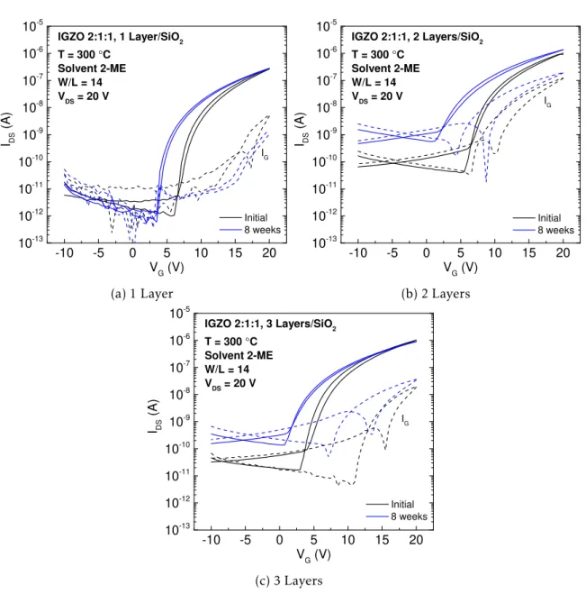
Figure 3.14: Transfer curves of IGZO 3:1:1 0.2 M TFTs with 1, 2 and 3 active layers, measured initially and 8 weeks later.
Table 3.7: Average and standard deviation of electrical parameters of three measured TFTs with IGZO 3:1:1 as channel layer, measured initially and 8 weeks later.
Layers Age Ion/Ioff Von(V) VT(V) VHyst(V) SS (V/dec) µsat(cm2V−1s−1)
1 Initial (1.99±0.57)×105 7.86±0.25 9.57±0.25 0.67±0.14 0.49±0.04 (1.00±0.03)×10−2 8 weeks (7.45±3.91)×104 5.71±1.01 8.67±0.48 0.64±0.03 0.69±0.12 (9.00±0.03)×10−3
2 Initial (5.31±2.54)×105 1.96±0.50 4.09±0.39 0.59±0.19 0.51±0.01 (6.67±0.94)×10−2 8 weeks (7.89±7.35)×104 0.18±0.44 2.29±0.61 0.49±0.12 0.76±0.17 (3.00±0.03)×10−2
3 Initial (8.17±3.48)×105 0.40±0.44 1.72±0.42 0.31±0.04 0.43±0.05 (7.33±0.47)×10−2 8 weeks (9.01±2.00)×103 −1.96±0.03 0.80±0.18 0.35±0.02 1.28±0.11 (5.00±0.03)×10−2
Regarding the effect of the number of semiconductor layers, it is noted that Von and
VTdecreased with the increasing number of layers, regardless the molar ratio composition.
These effects are essentially due to higher number of free carriers in the bulk of a thicker
3 . 3 . E L E C T R I CA L C H A R AC T E R I SAT I O N O F S O LU T I O N - BA S E D I G Z O T F T S
active layer, leading to an easier accumulation of charges in the semiconductor/dielectric interface. Thus, the formation of a highly conductive channel occurs at lower VGSvalues.
An increasing Ioffwith the number of layers is generally visible in transfer and stabilisation
curves, associated with the decreasing resistance of the active layer with increasing thickness, leading to a higher flow of electrons passing through source and drain electrodes [39]. The effect of the number of layers on Ion/IoffandSS is easily noted with the ageing effect, as it
will be explained further ahead.
Concerning composition effects, in IGZO TFTs 1:1:1 and 2:1:2 the performance of both
conditions was poorer than 2:1:1 and 3:1:1. In amorphous films, mobility is expected to increase for higherN, which increases for lower gallium or zinc concentrations. The Conduc-tion Band Minimum (CBM) is fundamentally composed by In3+, where potential barriers from random distribution of zinc and gallium exist; an increasingN leads to decrease in potential barriers from structural randomness, because higherN is associated with lower gallium and/or zinc content; also, it causes the dislocation of the Fermi level (EF) above these
potential barriers, enhancing mobility. Moreover, less zinc content increases the possibility of direct overlap of s-orbital of neighbouring In3+ions and hence enhances the mobility. Given this, the dominant-indium content is crucial for high-mobility IGZO TFTs, and gallium and zinc content should be in sufficient amount to prevent the crystallisation of the films and
guarantee the amorphous character of the structure. This sustains the low-mobilities and Ion/Ioffof IGZO 1:1:1 and 2:1:2 [2, 37].
TFTs with IGZO 1:1:1 2 and 3 layers, and IGZO 2:1:2 with 3 layers have shown high instability, which can be associated with their compositions combined with higher number of interfaces that are responsible for introducing more defects, leading to instability in the devices (see Appendix G).
TFTs with IGZO 1:1:1 1-layer possess low Ion/Ioffandµsat, due to high gallium content,
since it leads to suppression of free carriers, therefore for higher levels of gallium doping the electron transport is expected to degrade, decreasing both Ionand Ioff,µsat; VTand Von
have high values because these parameters are controlled byN. In TFTs with IGZO 2:1:2 the same principles are applied, combined with high content of zinc, leading to poorer electrical performance. [6, 26, 38].
For IGZO 2:1:1 and 3:1:1, the values ofµsat are generally higher, because as mentioned before, a composition with indium as dominating cation is fundamental to enhance mobility, since In3+spherical s-orbital has the largest radius of the three cations, thus the orbitals of neighbouring cations can easily overlap, allowing to create a good pathway for electron transport. Besides that, the higherN associated with higher indium content leads to higher Ion, resulting in higher Ion/Ioffvalues. Also, it facilitates the channel formation at lower VGS,
leading to a negative shift, which justifies the lower Vonand VT[7, 68, 69]. IGZO 2:1:1 and
3:1:1 TFTs have shown lower VhystandSS values than IGZO 1:1:1 and 2:1:2, meaning that a
composition with indium as dominant cation has a major role in these parameters.
In all casesµsathas very low values compared to the obtained in literature; in this work several factors could led to such results. Using SiO2as dielectric compared to high-k oxide