RBS-study of Ge
xSi
1-xCompounds Formed by Variable
Dose Ge Implantation into Si Wafers
A. Ramíreza, A. Zeheb*, A. Thomasc
aBenemérita Universidad Autónoma de Puebla, Instituto de Ciencias,
17 oriente # 1603, Puebla, Pue., México
bFacultad de Cs. Físico-Matemáticas, Apdo.
Post. # 1505, 72000 Puebla, Pue., México
cDisetronic GmbH, Sulzbach/Ts, Germany
Received: November 12, 2001; Revised: April 14, 2002
Amorphous and relaxed epitaxial GeSi films are prepared by Ge-implantation into Si(111) wafers of both 60 keV and 200 keV energetic Ge+-ions with appropriate dose, followed by
post-implantation thermal annealing, comprising a single final annealing at a temperature of 900 °C. The implantation dose was varied between 1014 and 1017 atoms cm-2. Rutherford backscattering
(RBS) and channeling analysis was applied in order to explore the formation of a single crystal-line Si-Ge compound layer, both prior and after the thermal treatment. The depth and the thick-ness of the implanted layer, as well as their molar composition and crystalline quality was deter-mined, and it was found that a single crystalline Si-Ge alloy layer was created, with both depth and mole fraction depending on the ion energy and the ion dose.
Keywords: Germanium implantation, solid phase epitaxy, Rutherford backscattering, sige/si heterostructure
1. Introduction
GeSi/Si heterostructure devices play an important role in microelectronics concepts since the heterojunction fab-rication technology has shown noticeable improvements. Unfortunately, difficulties with the incorporation of MBE or CVD based GeSi growth techniques into current very large scale integration schemes have shown to delay the com-mercialization of GeSi devices. An alternative approach for fabricating GeSi/Si heterostructures may be a technique based on high dose germanium ion implantation into sili-con, since ion implantation is a well established VLSI tech-nique characterized by a high wafer throughput. Up to now, ion implantation has been employed extensively in the ad-ditive microfabrication process of electronic devices, where the chemical, physical or electrical properties of semicon-ductors are altered by bombarding the substrate with high energetic ions of the appropriate chemical species. Adjust-ment of the ion energy allows to modify the range of the ions before they come to rest, permitting control of the depth distribution of the added material. Research on GeSi/Si
heterostructure materials has led recently to dramatic im-provements in performance and functionality of silicon-based electronic and optoelectronic devices1-5.
Germanium and silicon are miscible over the whole com-position range, thus GexSi1-x is an ideal material to study al-loy effects at any value of the mole fraction x. Over the past several years, advances in the Si/Ge technology have brought about an impressive potential for fabricating high-perform-ance Si/Si1-xGex heterojunction bipolar transistors6-8 as well as other Si/SiGe heterojunction devices9. However, even though Si/SiGe heterojunction devices can outperform bulk Si devices in a variety of aspects, the higher complexity and cost of Si/Ge epitaxial growth have yet prevented labo-ratory technologies from entering into high volume produc-tion10. Techniques like molecular beam epitaxy (MBE)11,12, low-pressure chemical vapor deposition (LP CVD) and ultrahigh vacuum chemical vapor deposition (UHV CVD)13-15, atmospheric pressure chemical vapor deposition (AP CVD)16 and very low pressure chemical vapor deposi-tion (VLP CVD)17 are intensely studied and have been dem-onstrated to deliver high quality heteroepitaxial materials in
try. Alternative methods for the production of single-crys-talline Ge-Si films were also developed. Abelson et al.18 produced epitaxial GexSi1-x /Si(100) structures by evaporat-ing Ge on Si(100) substrates and a subsequent laser beam mixing. The composition and the thickness of the alloy lay-ers depend on the deposited Ge film thickness and the laser power. A similar process is established by the irradiation of the Ge-Si system with an electron beam19. First results on the damage induced by Ge+-ion implantation into Si were reported by Mersey et al.20. The possibility of producing epitaxial GexSi1-x/Si structures by heavy-dose Ge+ -implan-tation and subsequent laser annealing was investigated in several occasions21-23. Multiple germanium implantation pro-vided also for a higher Ge incorporation26.
The aim of the present work is, to deal with the forma-tion of a single crystalline heterosystem GexSi1-x/Si(111) by Ge+-ion implantation into silicon wafers in dependence on ion energy and ion dose, respectively. Rutherford backscattering (RBS) and channeling technique is applied prior and after a thermal treatment in order to study the crys-talline character of the system.
2. Experiments
(111) oriented Si wafers, n-doped to reach a resistivity of 8 Ωcm, fixed with a small misorientation of about two degrees on a massive metal base without additional cooling were implanted with Ge+-ions at room temperature. The pressure in the ion accelerator was 1x10⁻⁴ Pa. Ions of two different energies were generated, 60 keV and 200 keV, re-spectively. The ion dose was varied between 1x10¹⁴ and 1x1017 cm-2 and applied while the beam was in a scanning mode. Thereafter the samples were annealed at 900 °C for 60 minutes in a nitrogen atmosphere. Prior to and after the annealing process the samples were studied with Ruther-ford backscattering spectroscopy (RBS), using 10.7 MeV 4He+-ions in both the random and the channeling (aligned)
crystal directions. The incident charge of the probing beam was 10 µAs, and the typical beam spot diameter was kept at 1 mm. The thickness and the depth of the implanted layer as well as their composition and crystalline quality were determined.
3. Results and Discussion
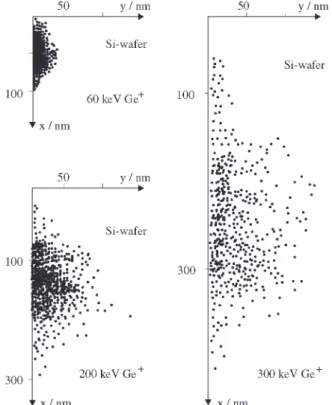
The distribution of the implanted germanium ions was calculated by the Monte-Carlo simulation program TRIM (transport of ions in matter)24 for three different ion ener-gies, 60 keV, 200 keV, and 300 keV, respectively, and is shown in Figs. 1 (a) and (b). The RBS spectra for the ‘as implanted’ samples with 60 and 200 keV Ge+-ion energies, are shown in the Figs. 2 and 3, respectively.
The random spectra are displayed only for the lowest
Figure 1a. Distribution in depth N(x) of implanted Ge+-ions into
Si, calculated by the simulation program TRIM24 with a step width
of ∆x = 10 nm. An implantation dose of 1017 cm-2 was chosen in
the calculus.
Figure 1b. Final position x of 500 implanted germanium ions as calculated by the simulation program TRIM24, applying ion
ener-gies of 60 keV, 200 keV, and 300 keV. The lateral y-distribution results from a projection of the spatial ion distribution onto the x-y
plane.
250 and 270. In this case the distribution of the damage resembles qualitatively the distribution of the implanted Ge+ -ions as calculated by the Monte Carlo simulation, shown in Fig. 1, and also derived from the RBS-plots of Figs. 2 and 3, as shown in Fig. 4.
With increasing implantation dose, the intensity of this Ge backscattering peak increases and broadens, suggesting that the depth of the damaged layer as well as the extent of damage increases. Such a behavior is very likely to be due to the recoil of the Si target atoms during implantation. In addition the shift of the Si peak detected for the highest doses implies that the Ge concentration close to the surface is significantly higher than for the other samples. This con-curs with the high intensity of the Ge peak, which was de-tected in the RBS spectra for a dose of 1x1017 cm-2 at chan-nel numbers 360 to 390. The width of this Ge peak reflects the depth of the Ge distribution. The deviation from the cal-culated distribution of Fig. 1 is probably caused by the dif-Figure 2. RBS-spectrum of a Si-sample, implanted with 60 keV Ge+-ions.
Figure 3. RBS-spectrum of a Si-sample, implanted with 200 keV Ge+-ions.
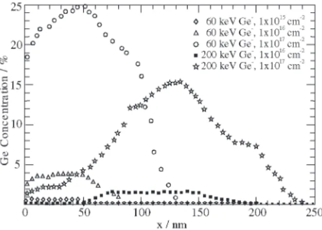
Figure 4. Ge concentration with respect to Si, derived from the RBS spectra shown in previous figures 2 and 3.
fusion of Ge atoms into the radiation damaged region. As a result the depth of the Ge distribution evaluated from the width of the Ge peak is almost identical to the depth of the radiation damaged region as measured by the width of the Si peak. This is supported by the Ge distribution derived from the RBS spectra in Fig. 4. Considering now the im-plantations at 200 keV ion energy, the RBS spectra of the ‘as implanted’ samples reveal a similar behavior. For the lowest dose the distribution of the damage is again in agree-ment with the calculated Ge distribution of Fig. 1. For the higher dose the width of the damaged layer is found to ex-ceed the width of the Ge distribution shown in Fig. 4. Con-sequently the Ge ions are supposed to be impaired of dif-fusing into the entire damaged region. As could be deduced from the fact, that the aligned yield reach the random value (Fig. 3) for the higher implantation doses, an amorphous layer seems to be formed. This is not in contrast with the fact that the He--probe ions originating from deeper regions show still channeling behavior25.
Pronounced differences are manifest in the RBS spectra of Figs. 5 and 6, representing the samples which were treated by thermal annealing.
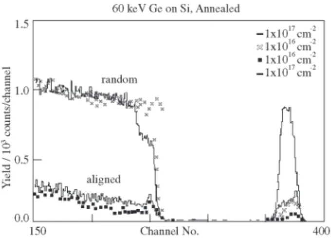
In the aligned spectra, the Si-peak denoting the radia-tion damage has now entirely disappeared in all cases. Ob-viously the crystalline structure was restored by the anneal-ing process. The crystalline quality of the Ge-Si alloy formed can be deduced from the cmin of the Ge peak. At a dose of 1x1017 cm-2, for instance, values of 17% and 22% were found for 60 and 200 keV, respectively. Furthermore, the line shape of this peak at 60 keV also indicates that the interface be-tween the Ge-Si alloy and the underlying Si substrate is very abrupt. This behavior is less pronounced for the RBS spectra given in Fig. 6.
Figure 7. Germanium distribution derived from the RBS spectra shown in previous Figs. 5 and 6.
Figure 6. RBS-spectrum of a Si-sample, implanted by 200 keV Ge+-ions and annealed at 900 °C for 60 minutes.
Ge atoms is essentially limited to the radiation-damaged region. Consequently homogeneous Ge distributions are achievable by annealing, which is clearly demonstrated in Fig. 7 by the data of the 60 keV samples.
4. Results and Discussion
A single-crystal quality Ge-Si alloy can be produced in Si substrates by Ge+-ion implantation and a subsequent ther-mal annealing process. We found a homogeneous distribu-tion of Ge in the layer between the Si surface and the maxi-mum penetration depth of implanted ions is. The stoichio-metric composition of the layer depends on the ion dose. By use of a fine-focus Ge+-ion beam, the formation of very small patterns within a Si substrate would be possible, turn-ing this approach potentially to a useful technique for three-dimensional microelectronic device integration. The
under-standing of key issues, such as diffusion kinetics of dopants in the Si-Ge region, device related material properties, such as carrier mobility and life time in implantation-formed Si-Ge are a future goal for the successful fabrication of ion implanted Si-Ge heterojunction transistors.
Acknowledgment
A.T. thanks Dr. Zahn, Berlin, R. Grötzchel and R. Klabes, Dresden-Rossendorf, for assistance in sample preparation and measurements. A.R. is indebted to CONACyT for pro-viding financial support through contract number 89628.
References
1. Umapathi, B.; Das, S.; Lahiri, S.K.; Kal, S. J. Electronic Materials, v. 30, p. 17-22, 2001.
2. Kwok, K.H. Solid-State Electronics, v. 43, n. 2, p. 275-283, 1999.
3. DiCaspare, L.; Capellini, L.; Cianci, E.; Evangelisti, F. J. Vac. Sci. Technol., v. B16(3), p. 1721, 1998.
4. Gluck, M.; Hackbarth, T.; Konig, V.; Haas, A.; Hock, G.; Kohn, E. J. Electron. Lett., v. 33, p. 325, 1997.
5. Mukarami, E.; Nakagawa, K.; Nishida A.; Miyao, M. IEEE Trans. Electron. Devices, v. 41 , p. 857, 1994. 6. Selvakumar, R.C.; Hecht, B. EDL, v. 12, n. 8, p.
444-446, 1991.
7. Schüppen, A.; Erben, U.; Gruhle, A.; Kibbel, H.; Schumacher H.; König, U. Proc. IEEE, IEDM 95 Tech. Dig., p. 743, 1995.
8. Kasper, E.; Kibbel, H.; Herzog, H.; Gruhle, A. J. Appl. Phys., v. 33, p. 2415, 1994.
9. Zhow, G.L.; Morkog, H. Thin Solid Films, v. 231, p. 125, 1993.
Figure 5. RBS-spectrum of a Si-sample, implanted by 60 keV Ge+
10. Wang, W.C.; Denton, J.P.; Neudeck, G.W.; Ming Lee, I.; Takoudis, C.G.; Koh, M.T.K.; Kvam, E.P. J. Vac. Sci. Technol., v. B15(1), p. 138, 1997.
11. Bean, J.C. J. Cryst. Growth, v. 81, p. 411, 1987. 12. Zehe, A. in: Crystal Growth and Charact. Adv.
Materi-als (A. N. Christensen ed.), World Scientific Publ., Sin-gapore 1987.
13. Cheung, W.Y.; Wong, S.P.; Wilson, I.H.; Zhang, T.; Chu, P.K. in: Beam-Solid Interactions for Materials Synthe-sis and Characterization, (eds. D. E. Luzzi, T. F. Heinz, M. Iwaki & D. C. Jacobson), Pittsburgh, PA, MRS Proc 354 (1995) 201-206.
14. Greve, D.W.; Raganelli, M. J. Vac. Sci. Technol., v. B8, p. 511, 1990.
15. Gronet, C.M.; King, C.A.; Opyd, W.; Gibbons, J.F.; Wilson, S.D.; Hull, R. J. Appl. Phys., v. 61, p. 2407, 1987.
16. De Boer, W.B.; Meyer, D.J. Appl. Phys. Lett., v. 58, p.286, 1991.
17. Jang, S.M.; Tsai, C.; Reif, R. J. Electron. Mater., v. 20, p. 91, 1991.
18. Abelson, J.R.; Sigmon, T.W.; Kim, K.; Weiner, K.H.; Appl. Phys. Lett., v. 52(3), p. 230, 1988.
19. Wada, T.; Takeda, M.; Yamada, T.; Ichimura, M. Appl. Surf. Sci., v. 41/42, p. 580, 1989.
20. Merzey, G.; Matteson, S.M.; Gyulai, J. Nucl. Instr. and Meth., v. 182/183, p. 587, 1981.
21. Cheung, W.Y.; Wong, S.P.; Wilson, I.H.; Zhang, T. Nucl. Instrum. & Meth, v. B 101, p. 243-246, 1995.
22. Berti, M.; Mazzi, G.; Drigo, A.V.; Migliori, A.; Jannitti, E.; Nicoletti, S. Appl. Surf. Sci., v. 43, p. 158, 1989. 23. Kwok, K.H.; Selvakumar, R.C. Proc. IEEE 1998
Cana-dian Conference on Electrical and Computer Engineer-ing, Waterloo, Canada, p. 878-881, May 1998. 24. Ziegler, J.F.; Biersack, J.P.; Littmark, U. The Stopping
Power and Ranges of Ions in Matter, Vol. I, Pergamon Press 1985.
25. Lu, X.; Cheung, N.W. Appl. Phys. Lett., v. 69, p. 1915, 1996.