756 Brazilian Journal of Physics, vol. 29, no. 4, December, 1999
Environment of Er in a-Si:H:
Co-Sputtering Versus Ion Implantation
Cnthia Piamonteze, Leandro R. Tessler,
Instituto de Fsica \Gleb Wataghin", UNICAMP, C. P. 6165, 13083-970, Campinas, SP, Brazil
M. C. Martins Alves, and H. Tolentino
Laboratorio Nacional de Luz Sncrotron, C. P. 6192, 13083-970, Campinas, SP, Brazil
Received February 6, 1999
We report a comparative Extended X-Ray Fine Structure (EXAFS) study of Er ina-Si:H prepared by Er implantation ina-Si:H and by co-sputtering undergoing the same cumulative annealing pro-cesses. It was found that the Er environment in as-implanted samples is formed by Si atoms, which are replaced by oxygen under annealing. In the co-sputtered samples, the initial low coordination oxygen environment evolves under thermal treatment to an Er2O3-like neighborhood.
I Introduction
The luminescence of triply ionized erbium (Er3+) in
semiconductors has motivated many studies of this sub-ject because of potential photonic applications. The Er3+ luminescence arises from atomic-like electronic
transitions within its incomplete 4f shell. An
emis-sion at s 1.54 m comes from the transition
be-tween the rst excited and the fundamental state (4
I 13=2
! 4
I
15=2) of the ion Er
3+. Since this
tran-sition does not involve bonding electrons and the 4f
shell is shielded by the outer 5s 25
d
6 shells, its energy
levels are relatively insensitive to the Er chemical neigh-borhood, i. e., depend very weakly on the host. The transition probability, however, depends on the sym-metry of the Er3+ site in the host. Intra-4
ftransitions
are electric dipole forbidden and only in a symmetry breaking environment the parity of the wavefunction is modied making the transition at least partially al-lowed. The wavelength of the photon associated to this luminescence (1.54m) is of particular interest because
it corresponds to the window of minimum absorption loss in silicon based optical bers. Silicon has been one of the most studied hosts for erbium because of the possibility of photonic-electronic integration. In sili-con, the luminescence intensity has been found to be strongly enhanced by the presence of impurities like
oxygen. Moreover, the Er3+ luminescence intensity is
higher in hydrogenated amorphous silicon (a-Si:H) than in pure crystalline silicon (c-Si) [1].
The chemical neighborhood of erbium has been in-vestigated in crystalline and amorphous silicon by Ex-tended X-Ray Absorption Fine Structure (EXAFS). It has been found [2] that ecient Er3+ luminescence in
Czochralski silicon (Cz-Si) is associated to an Er local environment very similar to that of Er2O3. In Er2O3
Er sits in a 6-fold coordinated cage, which according to [2] provides a non-centrosymmetric environment that allows the optical transition, in contrast to the highly symmetric 12-fold Si cage found in oat-zone silicon (FZ-Si), where the Er centers are optically inactive. An investigation [3] of annealing eects on crystalline Si co-implanted with Er and O, it has been found that the chemical environment of Er evolves from a 6-fold silicon coordination shell to a 5-fold oxygen coordination shell upon thermal annealing. In samples of non-annealed, co-sputtered Er doped a-Si:H and a-SiOx:H with
Cnthia Piamonteze et al. 757 study between Er in a-Si:H prepared by co-sputtering
and by Er implantation in sputtered a-Si:H. The evolu-tion of the Er chemical environment with thermal an-nealing in samples prepared by the two procedures un-dergoing the same cumulative annealing steps is found to be signicantly dierent.
II Experiment
An erbium doped a-Si:H sample was prepared in a con-ventional rf sputtering system following a procedure described elsewhere [5]. The oxygen to silicon concen-tration [O]/[Si] measured by Rutherford Backscattering spectroscopy (RBS) iss7.6 at. %, and [Er]/[Si] iss0.6
at. %. This high oxygen concentration is due to prepa-ration under sputtering conditions (low bias) leading to columnar a-Si:H, which optimize the Er3+
photolumi-nescence in samples not intentionally oxygenated [6]. The Er implanted a-Si:H sample was prepared under sputtering conditions optimized for good quality a-Si:H deposition. An Er concentration of 1016 cm,2, which
corresponds to [Er]/[Si]s0.2 at.%, was obtained by ion
implantation at IF-UFRGS, Porto Alegre, Brazil. The residual oxygen concentration in this sample is [O]/[Si]
s0.2 at.%, comparable to the Er concentration.
Erbium LIII-edge EXAFS was measured with
sec-ondary electron total yield detection at the XAFS beamline [7] of the Laboratorio Nacional de Luz Sncrotron (LNLS) in Campinas, Brazil. The samples were at room temperature during the measurements. Samples of bulk Er2O3 and a thin lm of ErSi2 were
used as reference standards for determining coordina-tion numbers and bond lengths. EXAFS data were processed following the recommendations of the Inter-national Committee [8].
The samples were annealed ex-situ in a nitrogen atmosphere at constant temperatures by 20 minutes steps. The temperatures used in the cumulative an-nealing varied between 200oC and 1100oC in
s100 oC
steps .
III Results
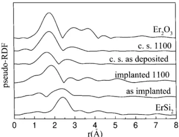
In gure 1 we show the pseudo-radial distribution func-tions (p-RDF) obtained from the Fourier transforms of
the EXAFS oscillations (k)k
2. Curves for the two
samples, as deposited and annealed at 1100oC, which
was the maximum temperature used, are represented.
Thep-RDF for the standard samples are also shown for
comparison.
Figure 1. Pseudo-RDF obtained from the k2 weighted
Fourier transforms. C. S. indicates the co-sputtered sam-ple. The annealing temperature is also indicated.
In the co-sputtered sample without thermal treat-ment and annealed the rst peak of thep-RDF indicates
an interatomic separation which is close to the Er-O distance in the standard Er2O3 sample. This indicates
that the erbium rst neighbors are oxygen atoms and they do not change under annealing.
The results for the implanted sample are quite dif-ferent. The rst peak of thep-RDF for the as implanted
sample is close to the Er-Si separation in ErSi2. The p-RDF is similar for all the annealing temperatures
except for the annealing at 1100oC, when it becomes
Er2O3 like. We can conclude that erbium is
coordi-nated to silicon up to annealing temperatures of 850oC.
Between 850oC and 1100oC it becomes coordinated to
oxygen.
To obtain the average atomic separation, the aver-age coordinations and the Debye-Waller factor relative to the rst neighbor shell we calculated the backtrans-forms of the isolated rst peaks of thep-RDF and
com-pared them with simulations using the amplitudes and phases obtained from the standard samples. The Er2O3
and ErSi2 standards were used for oxygen and silicon
neighbor shell respectively.
IV Discussion
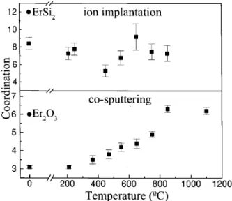
to-758 Brazilian Journal of Physics, vol. 29, no. 4, December, 1999 wards that of Er2O3, where erbium is coordinated with
6 oxygen atoms and the Er-O distance is 2.26A[2]. This can be seen in gures 2 and 3 where the average Er-O distance and erbium coordination are represented versus the annealing temperature. Both rst neigh-bor separation and coordination increase with anneal-ing temperature. The average Er coordination starts at 3.10.1 as in a-Si:H [4], reaches a maximumvalue of
6.30.3 for 850
oC annealing and remains at this value.
The maximum Er-O distance of 2.270.01A is reached
for 1100oC annealing.
Figure 2. Er rst neighbor separation in the implanted and co-sputtered samples. The values for ErSi2 and Er2O3
stan-dards are indicated.
Figure 3. Er coordination in the implanted and co-sputtered samples. The values for ErSi2 and Er2O3 standards are
in-dicated.
In contrast, the behavior of the average Er coordi-nation and rst neighbor separation with annealing is
very dierent for the implanted sample, as shown in g-ures 2 and 3. The Er-Si separation for the as deposited sample is 2.980.01A, very close to the Er-Si distance
in the standard ErSi2 which is 3.00A. This distance
starts to increase for annealing at 250oC and reaches
a maximum at 450oC (3.11
0.02A). At higher
anneal-ing temperatures the Er-Si distance remains constant. The Er coordination is approximately constant except for 450oC annealed sample, which shows a pronounced
decrease. The sample looked opaque after 550oC
an-nealing, indicating the onset of Si crystallization. The Er rst neighbor separation and coordination for 1100oC annealing are not shown in the gures
be-cause at this temperature the Er rst neighbor becomes oxygen. The value found for the Er-O separation in the implanted sample annealed at 1100oC is 2.28
0.02 and
the coordination is 6.50.6, indicating that the Er
lo-cal environment in this sample is very similar to that in Er2O3.
V Conclusions
In the sample prepared by co-sputtering, Er is incorpo-rated in such a way that it nds a conguration that minimizes the local free energy of the amorphous sys-tem. In this conguration, Er is surrounded in average by 3 oxygen atoms with an interatomic distance much smaller than in Er2O3 [4]. In the sample prepared by
ion implantation the violent Er incorporation does not allow system relaxation. Since the oxygen concentra-tion is small, Er is coordinated to silicon.
The expected eect of the annealing process is to let the system evolve to a lower free energy conguration. In the co-sputtered sample there is enough oxygen to satisfy the Er 6-fold coordination like in Er2O3. Thus
the Er chemical environment evolves to that found in this crystal. In the implanted sample, Er2O3-like
envi-ronment was only detected after annealing at 1100oC.
Observation of the sample in a microscope after this annealing step showed that parts of thea-Si:H lm had
been ablated. This probably opens easy oxidation ways allowing for the formation of Er2O3- like environments.
Cnthia Piamonteze et al. 759 the thermal treatment the host material relaxes by
cre-ating microvoids around the Er atoms. Consequently the Er coordination decreases and the Er-Si separation increases. For higher annealing temperatures silicon crystal nucleation starts causing an increase in the Er coordination whereas the Er-Si distance keeps approx-imately constant. Therefore, the local symmetry de-creases with annealing temperature until crystallization starts. This may be the reason why the maximumEr3+
photoluminescence is found for annealing temperatures below 500oC [9].
In summary, we have found that not only the Er chemical environment is dierent in the two as prepared samples but also that the evolution of this environment upon thermal treatment dier. The structural changes in the implanted sample lead to a more asymmetrical Er environment up to 450oC annealing. This enhances
the luminescence intensity. The Er chemical neighbor-hood in the sample prepared by co-sputtering evolves to that of Er2O3.
VI Acknowledgments
The authors are indebted to A. C. I~niguez for sam-ple preparation, to L. Amaral for ion implantation and to the LNLS sta for providing the photons. This
work was partially supported by FAPESP, CNPq and PRONEX \Fot^onica em Telecomunicac~oes ".
References
[1] M. S. Bresler, O. B. Gusev, V. Kh. Kudoyarova, A. N. Kuznetsov, P. E. Pak, E. I. Terukov, I. N. Yassievich, B. P. Zakharchenya, W. Fuhs and A. Sturm, Appl. Phys. Lett.67,3599 (1995).
[2] D. L. Adler, D. C. Jacobson, D. J. Eaglesham, M. A. Marcus, J. L. Benton, J. M. Poate, and P. H. Citrin, Appl. Phys. Lett.61, 2181 (1992).
[3] A. Terrasi, G. Franzo, and S. Coa, F. Priolo, F. D 'Acapito, S. Mobilio, Appl. Phys. Lett.70, 1712 (1997).
[4] C. Piamonteze, A. C. I~niguez, L. R. Tessler, M. C. Mar-tins Alves and H. Tolentino, Phys. Rev. Lett.81, 4652
(1998).
[5] L. R. Tessler and A. C. I~niguez, inAmorphous Silicon Technology -1998, (MRS Symp. Proc.507, Pittsburgh,
PA 1998), in press.
[6] L. R. Tessler and A. R. Zanatta, J. Non-Cryst. Sol.
227-230, 399 (1998).
[7] H. Tolentino, J. C. Cezar, D. Z. Cruz, V. Compagnon-Cailhol, E. Tamura, M. C. Martins Alves, J. Syn-chrotron Rad.5, 521 (1998).
[8] F. W. Lytle, D. E. Sayers, and E. A. Stern, Physica (Amsterdam)158B, 701 (1989).