Brazilian Journal of Physics, vol. 34, no. 2B, June, 2004 653
Electrical Properties of Bi-Doped PbTe Layers Grown by
Molecular Beam Epitaxy on BaF
2
Substrates
A.M.P. dos Anjos, E. Abramof, P.H.O. Rappl, A.Y. Ueta, and H. Closs
Laborat´orio Associado de Sensores e Materiais – LAS, Instituto Nacional de Pesquisas Espaciais – INPE,
CP515, 12245-970, S˜ao Jos´e dos Campos-SP, Brazil
Received on 31 March, 2003
Resisistivity and Hall measurements were performed at temperatures from 10 to 320K on Bi-doped PbTe layers grown on (111) BaF2 by molecular beam epitaxy. Samples with electron concentration varying from 1x10¹⁷
to 4x10¹⁹
cm−3were obtained. Results indicated that all offered Bi atoms in the vapor phase were effectively
incorporated in the PbTe as active donors. No thermal activation in the whole doping range was observed, indicating that the Bi donor level lies resonant with the conduction band. The mobility curve showed that the PbTe layers tend to a metallic behavior as the electron concentration increases. A value around 1x10¹⁹
cm−3
is suggested forn+PbTe contact layers in device application.
1
Introduction
The control of the electron concentration in PbTe layers is very desirable when device fabrication is concerned. In or-der to accomplish optimization of electrical performance, different carrier concentrations are needed in the several lay-ers that compose the device. The fabrication of a resonant tunneling double-barrier diode, for instance, requires lown -type PbTe near the barriers and high doping (n+)
in the bot-tom and top layers [1], and junctions likepn+
(orn+p)
are interesting for infrared detector application [2,3]. Bismuth is normally used as an n-type dopant in PbTe layers, and is usually evaporated from a Bi2Te3 source in a molecular
beam epitaxy (MBE) system [4].
In this paper, we investigate the electrical properties of Bi-doped PbTe layers grown on (111) BaF2substrates.
Re-sistivity, carrier concentration, and Hall mobility were mea-sured as a function of temperature for samples with differ-ent doping levels. The temperature dependdiffer-ent data allowed conclusions about the Bi impurity behavior in PbTe and the results supplied important information for the choice of the best doping condition for some device application.
2
Experimental
The PbTe layers were grown on freshly cleaved (111) BaF2
substrates by molecular beam epitaxy in a RIBER 32P MBE system equipped with effusion cells containing solid sources of PbTe, Te and Bi2Te3. The beam flux from each cell
was measured separately in an ion-gauge flux monitor. Dur-ing this experiment, the PbTe and Te effusion cell temper-atures were 656 ˚ C and 236 ˚ C, leading to beam fluxes of 7.2x10⁻⁷and 1.3x10⁻⁸Torr, respectively. The layers were always deposited at a substrate temperature of 300oC. In
these conditions the growth rate was 2.2 ˚A/s. In order to ob-tain the PbTe layers with different Bi doping levels, a series of samples were grown with Bi2Te3effusion cell
tempera-tures varying from 360 to 450oC.
For the electrical characterization, Van der Pauw geom-etry samples were prepared by soldering Au wires with In pellets. The samples were mounted in Ni-coated Cu-plates and assembled in a He closed-cycle cryostat equipped with an auto-tune temperature controller. The electrical measure-ments were performed in a Keithley Hall effect system with a magnetic field of 7000 Gauss. All equipments were com-puter controlled via an IEEE-488 interface. The control and data acquisition program, which allows automatic temper-ature dependent measurements, was developed in a Visual Basic platform.
3
Results and discussion
Resistivity and Hall effect were measured on the PbTe lay-ers grown at different doping levels at temperatures from 10 to 320K. Fig. 1 plots the electron concentration at 77K as a function of the Bi2Te3 effusion cell temperature. The
electron concentration follows approximately the same ex-ponential temperature dependence of the Bi2Te3vapor
pres-sure, indicating that, at this temperature range, the offered Bi atoms in the vapor phase are being effectively incorporated in the PbTe as active donors.
654 A.M.P. dos Anjoset al.
gap, the thermal activation of majority carriers is not ob-served in the undoped lead salts. For the case of the Bi-doped layers investigated here, the temperature dependence of the electron concentration did not exhibit any type of ther-mal activation in the whole doping range, as demonstrated in Fig. 2. This fact indicates that the doping level introduced by the Bi atoms also lies resonant with the conduction band.
350 400 450
1017 1018 1019 1020
n
( cm
-3 )
PbTe:Bi / BaF2
Bi
2Te3 temperature ( o
C)
Figure 1. Electron concentration at 77K of Bi-doped PbTe layers as a function of the Bi2Te3effusion cell temperature.
0 50 100 150 200 250 300
1017
1018
1019
1020
PbTe:Bi
n
(cm
-3 )
T (K)
Figure 2. Electron concentration versus temperature of PbTe lay-ers doped with bismuth. The stars are data from an undopedn-type
layer.
Since the carrier concentration almost does not change with temperature, the mobility in the lead salts is, in gen-eral, determined by the phonon scattering at temperatures higher than 80K. At low temperatures, the carrier scattering due to ionized impurities, which is normally observed for the most common semiconductor materials, is not present in the IV-VI compounds. The huge static dielectric constant, which screens the Coulomb potential of the impurities, and the relatively small effective masses are responsible for the high mobilities observed in PbTe at low temperatures. If well-controlled additional Te flux and elevated growth tem-peratures are used, low-temperature saturation mobility of above 106
cm2
/V.s is obtained inn-PbTe [5]. The mobility
saturation at low temperatures is related to carrier scattering due to defects, mainly dislocations.
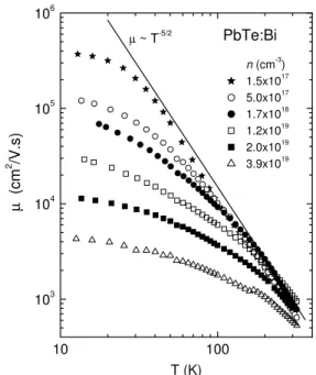
10 100
103 104 105 106
µ ~ T-5/2
n (cm-3)
1.5x10¹⁷
5.0x10¹⁷
1.7x10¹⁸
1.2x10¹⁹
2.0x10¹⁹
3.9x10¹⁹
PbTe:Bi
µ
(cm
2 /V.s)
T (K)
Figure 3. Hall Mobility versus temperature of PbTe:Bi samples with increasing electron concentration. Stars data belong to an un-doped sample.
Figure 3 shows the Hall mobility as a function of tem-perature for the PbTe layers with increasing Bi doping level. The data for an undopedn-type PbTe layer is also included. It is important to emphasize that the MBE growth condi-tions for the undoped and Bi-doped samples used in this work were not optimized to achieve the highest saturation mobility. Nevertheless, general features of the mobility curve as a function of electron concentration can be evi-denced. Although a pure metal-like PbTe is not observed in this set of samples, the PbTe layers tend to a metallic be-havior as the electron concentration increases. The phonon scattering limiting behavior (µ ∼ T−5/2), represented by the solid line in the graph, is observed at T > 100K for PbTe layers with nvalues up to 1x10¹⁸
cm−3. For higher electron concentrations, the mobility starts to deviate from this limit earlier at higher temperatures. At room tempera-ture, where phonons dominate over other scattering mech-anisms, the mobility shows a small decrease from 900 to 500cm2
/V.s, as the doping concentration increases from 1.5x10¹⁷
to 3.9x10¹⁹
cm−3. At an intermediate temperature of 80K, this reduction becomes more evident (27000 to 2100 cm2
/V.s), indicating that, at this temperature range, addi-tional carrier scattering processes start to limit the mobility as the carrier concentration increases. The low-temperature saturation mobility has the most pronounced reduction with electron concentration, as expected. It decreases from 4x10⁵
cm2
/V.s, for the undoped sample, to 4x10³
cm2
/V.s, for the sample withn=3.9x10¹⁹
Brazilian Journal of Physics, vol. 34, no. 2B, June, 2004 655
1017 1018 1019 1020
10-4
10-3 T = 77K
ρ
(
Ω
.cm )
PbTe:Bi
n ( cm-3 )
Figure 4. Resistivity as a function of electron concentration in PbTe layers with different doping levels.
In order to test the influence of the doping process on the crystalline quality of the samples, x-ray rocking curves were measured around the (222) Bragg diffraction peak of all samples. The full-width at half-maximum varied ran-domly from 70 to 140 arcsec, showing no influence of the Bi doping on the dislocation density in the PbTe layers. This result indicates that the pronounced reduction of mobility at low temperatures is only due to the substantial increase of the electron concentration.
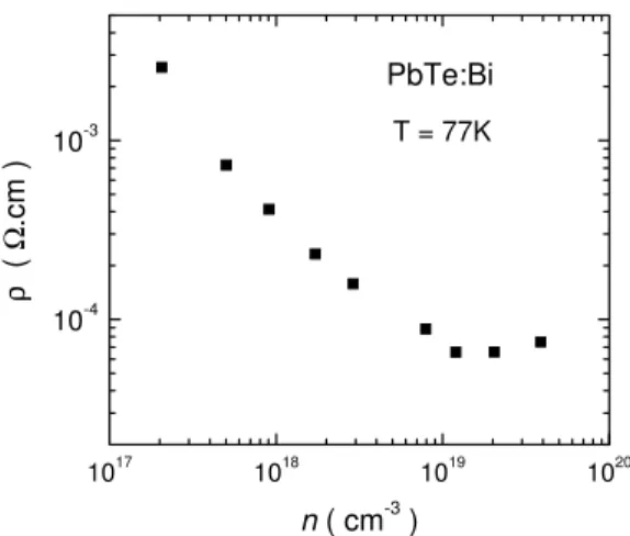
To find the best values forn+ PbTe contact layers, the resistivity at 77K (normal device operation temperature) is plotted in Fig. 4 as a function of electron concentration.
The resistivity decreases from approximately 3x10⁻³ to 6x10⁻⁵ Ω.cm as the electron density increases from 1x10¹⁷
to 1x10¹⁹
cm−3, and starts to rise slowly as more Bi atoms are incorporated. This result suggests a value around 1x10¹⁹
cm−3for then+-PbTe contact layers in device appli-cation.
Acknowledgement
We are grateful to partial support of FAPESP (Grant Nr. 00/12529-6) and CAPES (scholarship of first author).
References
[1] P. Han, M. Sakuraba, Y.-C. Jeong, K. Bock, T. Matsuura, and J. Murota, J. Cryst. Growth209, 315 (2000).
[2] J. John and H. Zogg, J. Appl. Phys.85, 3364 (1999).
[3] C. Boschetti, P.H.O Rappl, A.Y. Ueta, and I.N. Bandeira, In-frared Phys.34, 281 (1993).
[4] A. Prinz, G. Springholz, A.Y. Ueta, and G. Bauer, Phys. Rev. B59, 12983 (1999).