672 Brazilian Journal of Physics, vol. 34, no. 2B, June, 2004
MBE Growth and Characterization of Sn
1
−
x
Eu
x
Te
A. Y. Ueta
1, P. H. O. Rappl
1, H. Closs
1, P. Motisuke
1, E. Abramof
1, V. R. dos Anjos
2,
V. A. Chitta
3, J. A. Coaquira
3, N. F. Oliveira Jr.
3, and G. Bauer
41
Laborat´orio Associado de Sensores e Materiais, Instituto Nacional de Pesquisas Espaciais, Caixa Postal 515, 12245-970 S˜ao Jos´e dos Campos, S˜ao Paulo, Brazil
2
Epcar-Escola Preparat´oria de Cadetes do Ar, Barbacena, MG, Brazil
3
Instituto de F´ısica, Universidade de S˜ao Paulo, CP. 66318, 05315-970, S˜ao Paulo, SP, Brazil.
4
Institut f¨ur Halbleiterphysik, Universit¨at Linz, A-4040 Linz, Austria
Received on 31 March, 2003
Epilayers of Sn1−xEuxTe (0 < x < 0.03) were grown by molecular beam epitaxy on freshly cleaved
BaF2(111) substrates and their structural, electrical and optical properties were investigated. The thicknesses
of epilayers were about 1.5µm and deposition was carried out at growth temperatures of 300oC. The
struc-tural properties were investigated by high resolution X-ray diffraction and a sharp film degradation could be observed with increasing europium content. Electrical measurements with temperature varying from 300 to
10K indicated that the epilayers present carrier concentration ranging between3×1020and6×1020cm−3
and a low resistivity from6.3×10−5to1.2×10−4 Ω.cm. From optical measurements it could be seen that
spectra present a low energy edge corresponding to the beginning of intra band excitations and the high energy edge due to inter band excitations.
1
Introduction
IV-VI semimagnetic semicondutor compounds have been investigated by several groups in the last decades. The in-corporation of Eu, for instance in the lead salts has demon-strated to be useful for infrared optoelectronic applications, in particular for the fabrication of PbTe/PbEuTe hetero-junction diode lasers including quantum well structures [1]. SnTe is a IV-VI narrow gap semiconductor whose optical and electrical properties have been extensively investigated since the beginning of 1960’s [2-4]. In the case Sn1−xEuxTe alloys most of work has been focused in the magnetization studies in samples grown by Bridgman method [5-10]. A correlation between magnetic and electronic properties of Sn1−xGdxTe samples grown also by Bridgman method, has also been done [11-12]. In this work we present some results obtained in the investigation of structural, optical and elec-trical properties of Sn1−xEuxTe(0 < x < 0.03)epitaxial films grown by molecular beam epitaxy on freshly cleaved BaF2(111) substrates. Although SnTe and EuTe compounds
have the same crystal structure (FCC) and lattice mismatch about 4.3%, a complete miscibility is not expected for the whole composition range of Sn1xEuxTe alloy, because it would violate the well known 15% Hume-Rothery rule [13]. Table 1 summarizes some properties of SnTe and EuTe com-pounds.
2
Experimental Procedures
In order to investigate the peculiarities of this interesting Sn1xEuxTe pseudo-binary alloy various series of samples
Table 1. General properties of SnTe and EuTe
SnTe EuTe
Crystalline structure FCC FCC
Lattice constant ( ˚A) 6.327 6.598
Blin(K−
1
) 21.0×10⁻⁶ 13.6
×10−6
Density (g/cm3
) 6.45 6.45
Melting point (o
C) 806 2183
Energy Gap (eV) 0.3 (0 K) 0.18 (300 K) 2 (300 K)
were grown by molecular beam epitaxy in a Riber 32P sys-tem. The epilayers were fabricated by using three different effusion cells, which are able to evaporate SnTe, Eu and Te, separately. Prior the growth, freshly cleaved BaF2(111)
sub-strates were preheated at 200o
C during 30 min, in the prepa-ration chamber, and at 500o
C during 15 min, in the main chamber. The substrate holder was kept rotating during the growth to insure a reasonable thickness homogeneity for all samples. Epilayers of about 1.5µm thick were deposited
with growth rate of approximately 2 ˚A/s and substrate tem-perature kept at 300 o
C. The Volmer-Weber growth mode was observed by RHEED patterns for all samples.
A. Y. Uetaet al. 673
10K were performed Finally, a Fourier transform infrared spectrophotometer (Perkin Elmer – FTIR 1600) and a NIR-UV-VIS spectrophotometer (Hitachi – U3501) were used for optical transmission measurements at room temperature.
3
Results and Discussions
Although Sn1xEuxTe samples with x as high as approxi-mately 20% have been grown in this work, it could be ob-served by high resolution X-ray diffraction that a good crys-tal quality is achieved only for x values lower than 0.03, as can be seen in Fig. 1. This limitation is due to the fact that the difference between the atomic radius of Eu (2.04 ˚A) and Sn (1.62 ˚A) is more than 20%, which is much higher than the condition established by one of Hume-Rothery rules for solid solutions [13].
24,0 24,5 25,0 25,5
10-1
100
101
102
103
104 x=0
x=0.007 x=0.0019
x=0.03
BaF2
Intensity (cps)
(degrees)
Figure 1. X-ray data of the (222) diffraction peak for different
Sn1xEuxTe samples grown on BaF2(111).
Figure 2 shows that the lattice parameter increases from 6.327 to 6.368 ˚A as the Eu content varies from 0 to 0.022. It is important to notice that these alloys do not obey Vegard’s law. Actually the lattice constant considered for 0.03 is not so accurate because a phase separation is occurring probably due to spinodal decomposition [14], which is a well known phenomenon taking place in fluids, glasses and solids.
The crystal quality degradation is much more pro-nounced in Fig. 3, where it can be seen that the full width at half maximum (FWHM) varies from 164 to 571 arcsec for Eu content varying from 0 to 0.022. Again because the phase separation occurring in the sample with x=0.03 the FWHM is not so accurate.
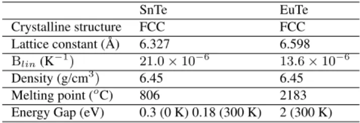
Figure 4 shows how the mobility varies as a function of temperature for samples with low Eu concentration, namely x=0.00017;0.0019;0.007; 0.022, respectively. It can be seen that the highest mobility (636 cm2
/V.s) is achieved at tem-peratures about 12K for the sample with x=0.00017. At room temperature the mobility of this sample decreases to 171 cm2
/V.s. Electrical measurements with temperature varying from 300 to 10K also indicated that the epilayers present carrier concentration ranging from 3 ×10²⁰ and
6×1020cm−3 and a low resistivity from 6.3 ×10⁻⁵ to 1.2×10⁻⁴ Ω.cm.
0,000 0,005 0,010 0,015 0,020 0,025 0,030 6,325
6,330 6,335 6,340 6,345 6,350 6,355 6,360 6,365 6,370
Lattice Parameter [Å]
nominal X
Figure 2. Lattice parameter of the Sn1−xEuxTe layers as a function
of nominal Eu content.
0,000 0,005 0,010 0,015 0,020 0,025 0,030 150
200 250 300 350 400 450 500 550 600
FWHM [arcsec]
nominal x
Figure 3. Full width at half maximum of the (222) x-ray rocking
curves for the Sn1−xEuxTe layers.
10 100
100
Mobility(cm
2/V
s)
Temperature(K)
x=0.00017 x=0.0019 x=0.007 x=0.022
Figure 4. Temperature dependence of Hall mobility for
Sn1
674 Brazilian Journal of Physics, vol. 34, no. 2B, June, 2004
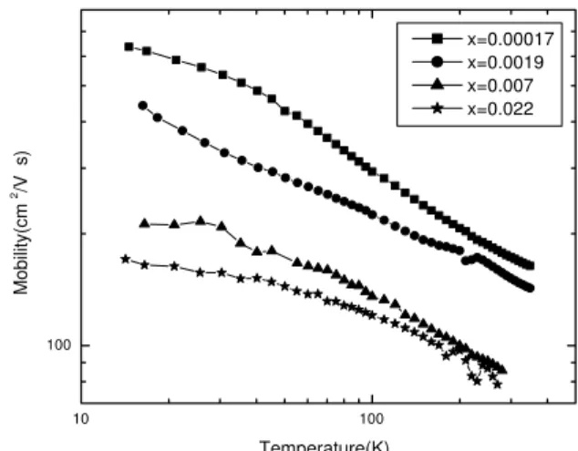
Due to high concentrations of holes in all samples the observed transmission spectra shown in the Fig. 5 present a low energy edge corresponding to the beginning of intra band excitations and the high energy edge due to inter band excitations.
1500 2000 2500 5000 6000
0 5 10 15
Trasmission (A.U.)
Wavenumber (cm-1 )
x=0,007 x=0,0018 x=0,00017 x=0 x=0,022
0,00 0,05 0,10 0,15
Figure 5. Transmission spectra at room temperature of the
Sn1
−xEuxTe layers.
4
Conclusion
In this work structural, electrical and optical properties of Sn1−xEuxTe(0 < x < 0.03)samples grown by molecu-lar beam epitaxy on freshly cleaved BaF2(111) substrates
were investigated. X-ray diffraction measurements indi-cated that layers with good crystalline quality were possible to be grown only for nominalx <0.03. Electrical measure-ments pointed out the increase of europium content in the lattice causes a drastic deterioration in the electrical prop-erties of the samples. A low energy edge corresponding to the beginning of intra band excitations and the high energy edge due to inter band excitations were observed by optical measurements.
Acknowledgements
The authors thank C. Kuranaga and P. G . Abramof for their helpful colaboration in doing some Infrared and X-ray measurements.
References
[1] D. L. Partin, Appl. Phys. Lett.45, 487 (1984).
[2] M. Cardona and D. L. Greenaway, Phys. Rev.133, A1685
(1964).
[3] J. R. Burke, Jr., R. S. Allgaier, and B. B. Houston, Jr., Phys.
Rev. Lett.14, 360 (1965).
[4] J. N. Zemel, J. D. Jensen, and R. B. Schoolar, Phys. Rev.140,
A330 (1965).
[5] J. R. Anderson, M. Gorska, Y. Oka, and J. Y. Jen, Solid State
Comm,96, 11 (1995).
[6] M. G´orska, J. R. Anderson, J. L. Peng, and Z. Golacki, J.
Phys. Chem. Solids Vol.56, 1253 (1995).
[7] M. G´orska, J. R. Anderson, J. L. Peng, and Z. Golacki, Acta
Phys. Pol. A84, 665 (1995).
[8] J. R. Anderson, M. G´orska, Y. Oka, J. Y. Jen, I. Mogi, and Z.
Golacki, Physica B216, 307 (1996).
[9] X. Gratens, E ter Haar, V. Bindilatti, N. F. Oliveira Jr, Y. Shapira, M. T. Liu, Z. Golacki, S. Charar, and A. Errebbahi,
J. Phys.:Condens. Matter12, 3711 (2000).
[10] A. Errebbahi, S. Charar, F. Terki, C. Fau, S. Isber, M. Tabbal, T. C. Christidis, D. Ravot, J. C. Tedenac, and Z. Golacki, J.
Magn. Magn. Mater.247, 55 (2002).
[11] T. Story, M. G´orska, E. Grodzicka, Z. Golacki, and R.R.
Galazka, J. Magn. Magn. Mater.140-144, 2041 (1995).
[12] M. G´orska, J. R. Anderson, C. Wolters, A. Lusakowski, T.
Story, Z. Golacki, Acta Phys. Pol. A94, 347 (1998).
[13] T. B. Massalski, inPhysical MetallurgyPart 1, eds. R. W.
Cahn and P. Hassen, 153 (1983).
[14] L. Salamanca-Young, D. L. Partin, and J. Heremans, J. Appl.