www.adv-radio-sci.net/14/85/2016/ doi:10.5194/ars-14-85-2016
© Author(s) 2016. CC Attribution 3.0 License.
Challenges and implementation aspects of switched-mode power
supplies with digital control for automotive applications
Samuel Quenzer-Hohmuth1, Thoralf Rosahl2, Steffen Ritzmann2, and Bernhard Wicht1 1Robert Bosch Center for Power Electronics, Reutlingen University, Reutlingen, Germany 2Robert Bosch GmbH, Automotive Electronics, Reutlingen, Germany
Correspondence to:Samuel Quenzer-Hohmuth ([email protected])
Received: 18 February 2016 – Revised: 13 May 2016 – Accepted: 25 May 2016 – Published: 28 September 2016
Abstract. Switched-mode power supplies (SMPS) convert an input DC-voltage into a higher or lower output voltage. In automotive, analog control is mostly used in order to keep the required output voltages constant and resistant to distur-bances. The design of robust analog control for SMPS faces parameter variations of integrated and external passive com-ponents. Using digital control, parameter variations can be eliminated and the required area for the integrated circuit can be reduced at the same time.
Digital control design bears challenges like the preven-tion of limit cycle oscillapreven-tions and controller-wind-up. This paper reviews how to prevent these effects. Digital trol loops introduce new sources for dead times in the con-trol loop, for example the latency of the analog-to-digital-converter (ADC). Dead times have negative influence on the stability of the control loop, because they lead to phase de-lays. Consequently, low latency is one of the key require-ments for analog-to-digital-converters in digitally controlled SMPS.
Exploiting the example of a 500 kHz-buck converter with a crossover frequency of 70 kHz, this paper shows that the 5 µs-latency of a 16-analog-to-digital-converter leads to a reduction in phase margin of 126◦. The latency is less critical for boost converters because of their inherent lower crossover frequencies.
Finally, the paper shows a comparison between analog and digital control of SMPS with regard to chip area and test costs.
1 Introduction
The increasing need for cost pressure for automotive manu-facturers and suppliers leads to steadily rising requirements for various electronics components in cars. The components should get smaller, lighter and cheaper while maintaining equal performance. This affects also switched-mode power supplies, which are installed for the generation of voltage supplies with different voltage levels in cars. In order to offer a small-sized realization of SMPS there are numerous ap-proaches. There are attempts to tune the switching frequency in order to reduce the size of the discrete components such as the inductor (Wittmann and Wicht, 2013). There are also attempts to improve the dynamic behavior of the closed loop system using digital control. This is one of the reasons why digital control of SMPS experiences growing demand.
Digital control offers several advantages compared to ana-log control. Digital control is not restricted to pure linear con-trol like analog concon-trol is. He and Xu (2007) have shown that nonlinear control has dynamic advantages compared to linear control and enables rapid compensation of load transients.
Parameter variations of compensation devices, which are necessary to adjust the dynamic behavior of an analog con-troller, and parameter variations of the LC-filter lead to dif-ficulties designing the analog control. Varying values of the compensation devices result in uncontrolled variations in fre-quency characteristics of the analog controller. With a digital control there are no compensation devices and thus no vari-ations in frequency behavior. Furthermore, in an integrated solution chip size and thereby costs decrease.
stabiliz-ing the crossover frequency and phase margin of the closed-loop system, as presented by Morroni et al. (2009).
This paper presents a digitally controlled boost converter and shows why digital control for a buck converter with a 16-analog-to-digital-converter with 5 µs-latency is not achievable. Besides, it shows how to prevent limit cycle os-cillations (LCOs) and controller wind-up. A comparison of chip size and test costs of the digitally controlled boost con-verter with an analog controlled boost concon-verter concludes the paper.
2 Challenges and implementation aspects
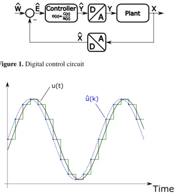
In order to digitally control a SMPS, additional components are required, namely an analog-to-digital-converter and a digital-to-analog-converter (DAC). In return, the realization of the controller is easier and needs less hardware (no com-pensation devices) than an analog controller. With these addi-tional components the control loop is built as shown in Fig. 1. SignalXcorresponds to the output voltage of a SMPS which is typically scaled down to a lower voltage with a resistor feedback divider and then converted into a digital valueXˆ. SignalYˆis the digital controller output value.Y correlates to the PWM signal which is necessary to control the switch of the SMPS.
2.1 Phase delays
In digital control loops there are sources for dead times, for example the latency of the analog-to-digital-converter and of the digital-to-analog-converter or the calculation time of the digital controller. The sampling with finite sample time can be modeled with a correlating dead time.
Dead times degrade the stability of the control loop be-cause they introduce unwanted phase shifts. As a result, dead times reduce the phase margin, which causes a less damped or even unstable control loop. The relation of dead timeTd and phase shift1ϕshows Eq. (1):
1ϕ= −ω·Td (1)
2.1.1 ADC and DAC caused dead times
Analog-to-digital-converters need time for the conversion of the analogous input voltage to a digital output value. The same applies for the digital-to-analog-converter. Depending on the converter architecture greater or smaller dead times result. This latency appears as dead time for the control loop. Another source of a dead time is the calculation time of the controller output value.
2.1.2 Sampling caused delay
In a digital control circuit the output signal is sampled and processed from the controller. Afterwards it is hold till the
Controller
Plant D
A
D A
W E Y Y X
X
D(z)= N(z) C(z)
Figure 1.Digital control circuit
Time
u(t)u(k)
Figure 2.Sampling caused delay
next sample is taken and processed. This behavior is modeled with a zero-order-hold. Since the zero-order-hold is not a lin-ear time-invariant system, there is no possibility to determine a transfer function. But with the help of a sinusoidal stimulus and the help of the resulting signal response it is possible to find a proper model for the zero-order-hold (Lunze, 2010).
If the input signal of the zero-order-hold is the sinusoidal sequenceu(k)ˆ =sin(kT ), it will generate a continuous step function as shown in Fig. 2.
The input of the controlled system is the step function, which contains a wide spectrum of frequencies. Most con-trolled systems have low-pass characteristics, thus the high frequencies of the step function will not be transmitted and can therefore be disregarded for modeling. The small fre-quencies (especially the fundamental frequency) have to be considered. The fundamental frequency after Fourier anal-ysis, in case the sampling theorem is satisfied, can be de-scribed as Eq. (2) shows.
u(t )=2·sin(0.5·T )
T ·sin(t−Td) (2)
This shows that the zero-order-hold has a gain, which is nearby 1 and hence, not relevant. On the other hand there is a significant delay. The resulting delayTdas a function of the sampling rateT is approximately:
Td=
T
2.2 Limit cycle oscillations
The quantization introduced through the ADC and the DAC can lead to limit cycle oscillations. Limit cycle oscillations are steady-state oscillations of the output voltage at lower frequencies as the switching frequency of the converter (Pe-terchev and Sanders, 2001).
2.2.1 Resolution caused LCOs
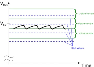
Due to the quantization of the output voltage through the analog-to-digital-converter there is an analogous voltage range with the width of one LSB (hereinafter called “bin”) for each digital value. Thus there is an analogous voltage bin for the digital set point (0-bit-error-bin). If the output voltage is located in this bin, the control error will be zero. Premise for permanent elimination of the control error is that there is a digital-to-analog-converter value (DAC-value) which forces the output voltage to stay within the 0-bit-error-bin. To fulfill this premise the resolution of the digital-to-analog-converter referred to the output voltage has to be higher than the resolu-tion of the analog-to-digital-converter referred to the output voltage.
Resolution (DAC)>Resolution (ADC) (4) If this condition is not met, there will not be a DAC-value for every output voltage bin. Figure 3 shows what will hap-pen if the above mentioned condition is not taken into ac-count. There is no DAC-value which leads to a voltage within the 0-bit-error-bin. That is why the output voltageVoutdoes not stay permanently within the 0-bit-error-bin and a limit cycle oscillation arises.
2.2.2 Missing integral term caused LCOs
If the controller has no integral term, limit cycle oscillations can occur regardless of the condition given in Eq. (4). This issue is shown in Fig. 4. As long as there is a control error the controller tries to drive the output voltageVouttowards the error-bin. As soon as the output voltage reaches the 0-bit-error-bin the control error gets zero. Without integral term in the controller the DAC-value changes immediately and as a consequence the output voltage leaves the 0-bit-error-bin again.
To avoid this kind of limit cycle oscillations the controller requires to have an integral term.
2.2.3 No limit cycle oscillations
Beside the cases shown in this paper, Peterchev and Sanders (2001) as well as Peng et al. (2004) show further special cases leading to limit cycle oscillations.
If all conditions for no limit cycle oscillations are met, the output voltage will stay within the 0-bit-error-bin in steady-state. If the controller has an integral term, the digital value
Time Vout
Vsp
}
}
}
-1-bit-error-bin
0-bit-error-bin
1-bit-error bin
DAC-values
Figure 3.Resolution caused limit cycle oscillations
Time Vout
Vsp
}
}
}
-1-bit-error-bin
0-bit-error-bin
1-bit-error-bin
DAC-values
Figure 4.Missing integral term caused limit cycle oscillations
Time Vout
Vsp
}
}
}
-1-bit-error-bin
0-bit-error-bin
1-bit-error-bin
DAC-values
Figure 5.No limit cycle oscillations
2.3 Controller wind-up
In a digital control loop controller wind-up is possible if the controller has an integral term, which is necessary for avoid-ing limit cycle oscillations. This unwanted effect can be elim-inated using a dedicated anti-wind-up controller structure. 2.3.1 Controller wind-up mechanism
In a digital control loop (see Fig. 1) the digital controller out-put signal is converted by a digital-to-analog-converter into an analogous signal. This DAC has an input range, hence the DAC-value cannot get as high nor as low as it would be required. The value calculated from the controller can thus be higher than the DAC-value appearing at the plant. Conse-quently, in case of large control deviation the output voltage does not move back to the set point as fast as the controller scheduled it.
The controller integrates the control deviation and the cal-culated value now gets even higher than before. But the digital-to-analog-converter still does not allow the DAC-value seen from the plant to get any higher.
The controller further integrates until the control devia-tion changes in sign. This happens because the controller has counteracted the control deviation, the DAC has only limited the power to do so. The large controller output value needs to be integrated into the opposite direction to get back into the input range of the DAC. This delaying effect leads to long lasting and huge control deviations.
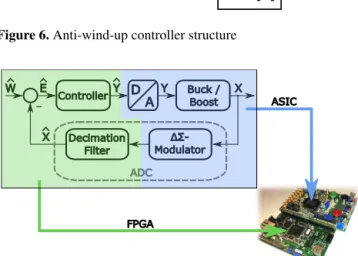
2.3.2 Anti-wind-up controller structure
Controller-wind-up can be counteracted with an anti-wind-up controller structure. The anti-wind-anti-wind-up controller structure, as shown in Fig. 6, is modified marginally compared to a standard controller.
The original controllerD(z)is divided in numerator and denominatorD(z)=Y (z)ˆˆ
E(z) = C(z)
N (z). With this partitioning the
anti-wind-up controller structure can be built as shown in Fig. 6 with only one more block compared to a standard architecture (Fig. 1). This block is a limitation block with the limits matching to the limits of the digital-to-analog-converter (or any other limiting element).
It can be shown thatV (z)ˆ corresponds to the original con-troller output signal in the case thatV (z)ˆ is within the limits of the limitation block. ThenV (z)ˆ = ˆY (z)is valid.
ˆ
V (z)= ˆV (z)·(1−N (z))+C(z)· ˆE(z) (5) By manipulating the equation, it can be shown that this modified anti-wind-up controller structure matches to the original controller.
D(z)= ˆ
Y (z)
ˆ
E(z)
=C(z)
N (z) (6)
C(z)
V(z)E(z) Y(z)
1-N(z)
Figure 6.Anti-wind-up controller structure
Decimation Filter
Buck / Boost D
A
W E Y Y X
X
Controller
ΔΣ -Modulator
ADC
ASIC
FPGA
Figure 7.Measurement setup for SMPS with digital control
IfV (z)ˆ crosses a limit of the limitation block (and thus the limit of the digital-to-analog-converter) this internal limita-tion block prohibits further growth of the controller output. Further integration is stopped although a control deviation is still existent. Once the control deviation changes in sign the controller reacts immediately (in contrast to the standard controller architecture).
Further information on controller wind-up can be found in Schulz and Graf (2013).
Table 1.Parameters of ADC and DAC
Parameter ADC DAC
Architecture: 16 R-2R
Resolution: 10 bit 10 bit
18 mV LSB−1 12 mV LSB−1
Latency: 5 µs n/a
Sampling rate: 400 kSps 400 kSps
Table 2.Parameters of buck and boost converter
Parameter Buck Boost
Input voltage: 14 V 3.5 V
Output voltage: 6 V 6.3 V
Switching frequency: 500 kHz 500 kHz
Crossover frequency: 70 kHz 2 kHz
Table 2 presents information about the boost and buck con-verter.
3.1 Buck converter
As the latency of the analog-to-digital-converter isTd=5 µs the phase delay for a crossover frequency offc=70kH zcan be calculated with Eq. (1).
1ϕ= −ω·Td= −2·180◦·70 kHz·5 µs= −126◦ (7) In addition there is the inherent delay through sampling. With Eq. (2) the effective dead time results inTd=T /2= 1.25 µs. Accordingly, the phase delay gets1ϕ= −ω·Td= −2·180◦·70 kHz·1.25 µs= −31.5◦. Adding the two phase delays the total phase delay reaches1ϕtot= −157.5◦. This total phase delay is very high and therefore digital control for a buck converter with 70 kHz crossover frequency and with the available 5 µs-latency analog-to-digital-converter is not possible. This buck converter with digital control could either be realized with a low-latency ADC or an ADC dedicated for digital control of SMPS, as proposed by Lukic et al. (2007). 3.2 Boost converter
In comparison to the buck converter, the boost converter has an inherent lower crossover frequency because of its right-half-plane zero (Basso, 2008). Thus the latency of the analog-to-digital-converter has less influence on the phase delay 1ϕ= −ω·Td= −2·180◦·2 kHz·5 µs= −3.6◦. Ac-cordingly, the sampling caused phase delay is less, too:1ϕ= −ω·Td= −2·180◦·2 kHz·1.25 µs= −0.9◦. The total phase delay is1ϕtot= −4.5◦and, consequently, digital control for a boost converter is possible without major impact on stabil-ity.
Figure 8 shows measurement results for the presented boost converter in case of a load transient. The output voltage
0 0.5 1
6 6.1 6.2 6.3 6.4 6.5 6.6 6.7
Time in ms
O
ut
put
vo
lt
age
in
V
olt
s
Figure 8.Measured load transient of the presented boost converter
(Iload=160 mA→Iload=60 mA)
Figure 9.Test costs and chip area of digital and analog control in
comparison
recovers safely from the load transient, thus, the latency has no impact on the stability of the boost converter.
4 Comparison between analog and digital control This section shows a comparison of chip area and test costs necessary for the integration of the control for a boost con-verter. The comparison is elaborated on the one hand for an analog control used in a conventional automotive chip and, on the other hand, for a digital control with comparable char-acteristics. The comparison does not consider the total area of the converter, it considers only the diverging parts in analog and digital control. Thus, for digital control only ADC, dig-ital controller and DAC are considered. For the analog con-trol only the error amplifier including compensation compo-nents (two capacitors and one ohmic resistor) are considered. These components are necessary in analog control to realize a controller with the same frequency characteristic as the pre-sented digital controller.
4.1 Test costs
test costs for the analog control. The tests for the analog con-trol involve especially error amplifier testing, for example measurement of the transfer characteristic and measurement of the operating range. For the digital control, typical dig-ital tests like stuck-at-fault and Iddq-measurements are per-formed. The results show that test costs for the digital control are 85 % lower, compared to analog control.
4.2 Chip area
The considered digital control offers more flexibility than the analog control. The digital controller coefficients are imple-mented to be flexible. Area effort is much higher for variable coefficients than for fixed coefficients. In return, variable co-efficients allow to change the dynamic behavior of the con-trol loop in operation.
Figure 9 shows that the implementation area of the digital control of a boost converter is significantly smaller than the layout area of the analog control of a fully-integrated boost converter (incl. passives of the control loop). Furthermore, the digital control offers more dynamic flexibility in opera-tion.
5 Conclusions
This paper presents that limit cycle oscillations can be pre-vented by securing that the resolution of the DAC is higher than the resolution of the ADC and by implementing a controller with integral term. Furthermore, controller-wind-up can be prevented by the implementation of a dedicated anti-wind-up controller structure with a limiter block. Digital control circuits contain sources for latency, such as the analog-to-digital-converter and the digital-to-analog-converter. Latencies impact the stability of the control loop. The example of a 500 kHz-buck converter with a crossover frequency of 70 kHz shows that digital control cannot be realized with a 5 µs-latency16-analog-to-digital-converter. Consequently, a low latency is one of the key requirements for analog-to-digital-converters. A comparison of analog and digital control indicates that chip area (60 %-reduction) and test costs (85 %-reduction) for switched-mode power supplies can be reduced by digital control. At the same time flexibility in operation can be achieved with variable
controller coefficients. Thus, adaptive, nonlinear, and dynamic-optimized control can be realized. Switched-mode power supplies with digital control show high potential for value-added power management systems in automotive ICs.
Edited by: D. Killat
Reviewed by: two anonymous referees
References
Basso, C. P.: Switch-Mode Power Supplies: SPICE Simulations and Practical Designs, The McGraw-Hill Companies, New York, USA, 2008.
He, M. and Xu, J.: Nonlinear PID in Digital Controlled Buck Converters, in Applied Power Electronics Conference, APEC 2007 – Twenty Second Annual IEEE, 1461–1465, doi:10.1109/APEX.2007.357709, 2007.
Lukic, Z., Rahman, N., and Prodic, A.: Multibit Sigma-Delta PWM Digital Controller IC for DC-DC Converters Operating at Switching Frequencies Beyond 10 MHz, IEEE T. Power Electr., 22, 1693–1707, doi:10.1109/TPEL.2007.904199, 2007. Lunze, J.: Regelungstechnik 2, Springer Verlag, Berlin Heidelberg,
Germany, 2010.
Morroni, J., Zane, R., and Maksimovi´c, D.: Design and Implemen-tation of an Adaptive Tuning System Based on Desired Phase Margin for Digitally Controlled DC-DC Converters, IEEE T. Power Electr., 24, 559–564, doi:10.1109/TPEL.2008.2007641, 2009.
Peng, H., Maksimovi´c, D., Prodi´c, A., and Alarcón, E.: Modeling of Quantization Effects in Digitally Controlled DC-DC Converters, IEEE 35th Annual Power Electronics Specialists Conference, 2004 (PESC), 6, 4312–4318, doi:10.1109/PESC.2004.1354763, 2004.
Peterchev, A. V. and Sanders, S. R.: Quantization Resolution and Limit Cycling in Digitally Controlled PWM Converters, IEEE 32nd Annual Power Electronics Specialists Conference, 2001 (PESC), 2, 465–471, doi:10.1109/PESC.2001.954158, 2001. Schulz, G. and Graf, K.: Mehrgroessenregelung, Digitale
Regelung-stechnik, Fuzzy-Regelung, Oldenbourg, Munich, Germany, 2013.