A Comparitive Study of On-Chip Clock
Generators Using a-IGZO TFTs for Flexible
Electronic Systems
Nishtha Wadhwa
a, Jorge Martins
b, Pydi Bahubalindruni
a, Sujay Deb
a, Pedro Barquinha
b a IIIT-Delhi, Okhla Industrial Estate, Phase III, New Delhi, India - 110020b i3N/CENIMAT, Department of Materials Science and Technology,
Universidade NOVA de Lisboa and CEMOP-UNINOVA, Campus de Caparica, 2829-516 Caparica, Portugal
Abstract—This paper presents a comparitive study of ring oscillators (RO) using amorphous Indium Gallium Zinc Oxide (a-IGZO) thin-film transistors (TFTs) to imple-ment on-chip clock generator for flexible electronic systems. A five-stage RO has been implemented with different inverter topologies using IGZO TFTs, which includes Diode connected load, Capacitive bootstrapping (BS), Pseudo-CMOS and Pseudo-Pseudo-CMOS bootstrapping architectures. These topologies have been simulated using in-house IGZO TFT models under similar conditions using different power supplies (10 V, 15 V and 20 V) in cadence environment. Among all architechtures Capacitive bootstrapping RO has ensured highest frequency of operation in the order of MHz and an output swing of 82% of VDD. Whereas,
Pseudo-CMOS based RO provides the lowest power consumption in the order of µW with an output swing of 57% of VDD.
On the other hand, the combination of Pseudo CMOS and bootstrapping has ensured highest voltage swing of 95% of VDD. In terms of power delay product (PDP)
BS RO is superior with respect to other topologies. This work provides a clear insight to the designer to choose a particular topology for given application, mainly for on-chip clock generation for flexible electronic systems based on the requirements.
Keywords—Ring Oscillator, a-IGZO TFTs, Bootstrap-ping, Pseudo-CMOS, Flexible on-chip clock generator.
I. INTRODUCTION
Amourphous Indium Gallium Zinc Oxide (a-IGZO) thin-film transistors (TFTs) are the ideal candidates to implement flexible electronics due to their compatiblity with low temperature fabrication process (180◦C) by allowing various substrates, such as, plastic, fibre or paper [1], [2]. Other advantages of a-IGZO TFTs include uniformity over large areas, relative high mobility (>10 cm2/Vs), reliability and compatibility with low cost fabrication techniques. Because of these properties they are gaining significant interest in various real world applications, namely smart packaging, biomedical wear-able systems [3], Near-Field Communication (NFC) [4] and Radio Frequency Identification (RFIDs) [5]. On-chip clock generator is one of the essential block to implement
these systems. However, the absence of stable and repro-ducible p-type oxide TFT, impose limitation on circuit design and CMOS design techniques cannot be adapted directly. Therefore, circuit design should take place only with n-type transistors. Nevertheless, many ROs have been reported till date with a-IGZO TFTs [1], [6], [7], [8], [9], [10]. Absence of complementary devices lead to poor noise margin [11], which results in the degradation of output swing when such multiple stages are used in cascade [12]. In addition, this also leads to high static power consumption. Many designs using monotype TFTs have been proposed to address above challenge (mainly output swing), such as, depletion load [13], [14], dual gate [11], [15], dual VT TFTs [16]. These tech-niques have limited applicability due to the requirement of dedicated TFT characteristics, additional masks and fabrication processing steps. It is very challenging to achieve CMOS characteristics with these Amorphous Oxide Semiconductors (AOS) [17], [18]. In addition, some of the hybrid structures have also been proposed with n-type AOS and p-type organic/carbon nanotube TFTs [19]. However, it is relatively expensive and com-plicated to fabricate these hybrid structures due to differ-ent processing conditions [15], [20], [21]. It should also be noted that, even if the circuits are implemented only with n-type oxide TFTs, it is hard to compare the circuit performance as there is no international standardization for oxide TFT technology unlike standard CMOS. For this technology different Fabs use different processing steps, device structures and materials [3], [9], [10], [22]. Therefore, for a given application it is hard to choose the most suitable on-chip clock generator (RO) architecture that can give the desired performance.
In order to address this challenge, this work presents a comparitive study of ROs with a-IGZO TFTs that are implemented and simulated under same conditions using different inverter topologies. This can provide clear insight to the designer so that a proper RO architecture can be selected based on the specific application require-ments. The main topologies that are considered in this study are diode connected RO [23], [24], Bootstrapped
RO [9], Pseudo-CMOS RO [6], [22] and the combina-tion of Pseudo-CMOS bootstrapped RO [8], [10]. All the circuits have been simulated using in-house TFT models at different power supply ranging from 10-20 V [25], [26]. The simulation outcome has demonstrated that bootstrapped RO can be used for high frequency applications and pseudo-CMOS can be used for low-power applications. While both these ROs have shown a limited output voltage swing, a third topology combining Pseudo-CMOS and bootstrapped RO offers a significant improvement on this, without compromising frequency and power consumption.
The rest of the paper is organised as follows. Section II discusses the fabrication details of TFTs and in-house TFT model. Section III demonstrates the circuit descrip-tion and its operating principle. Secdescrip-tion IV presents the simulation results and discussions and finally the conclusions are drawn in section V.
II. FABRICATION OF A-IGZO TFTS
Gate, source and drain electrodes were deposited by a 60 nm thick Mo layer using RF magnetron sputtering, being the same technique used to deposit the 40 nm thick semiconductor (IGZO) layer. 250 nm thick dielectric following a multilayer approach consisting of SiO2 + Ta2O5.SiO2 + SiO2 was then RF sputtered and patterned using reactive ion etching. At the end devices were annealed at 180◦C in air for 1 hour. Transistors have inverted staggered bottom gate structure. The fabrication processes described above can be used for device fab-rication on glass or PEN, with both substrates resulting in similar TFT performance. A micrograph of a-IGZO TFT is presented in Fig. 1.
TFTs were characterised with a Keysight B1500A semiconductor analyzer and a Cascade EPS-150 probe station under dark room conditions. I-V and C-V mea-surements were then used to develope a VerilogA model based on artificial neural networks (ANN), in order to enable circuit simulation in Cadence environment [26].
Pads Gate
Vias Source Drain
250 µm
Fig. 1. Micrograph of single a-IGZO TFT [26]
III. CIRCUITDESCRIPTION
A ring oscillator is comprised of an odd number of inverters connected in series and then back-coupled to provide an unstable state that leads to oscillations [27]. The conventional CMOS based RO consists of both PMOS and NMOS transistors, while in current work, all designs have been implemented with a-IGZO TFTs, which are inherently n-type in nature. A 5-stage RO has been considered in this work as shown in Fig. 2, where an inverter is an essential block. This inverter design dictates overall performance of the ring oscillator. Therefore, different implementations of inverters based on only n-type transistors are discussed below, as a first step.
Fig. 2. Schematic of 5-stage RO
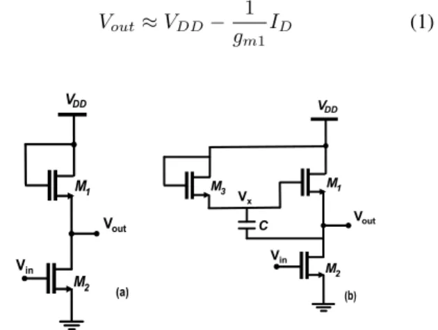
1. DIODE CONNECTED INVERTER: The circuit schematic with diode load is presented Fig. 3(a). In this both M1 and M2 have same channel length, while WM 2 > WM 1 to favour voltage swing. In this, if the input voltage (Vin) is set to a low value, M2 is almost turned off and nearly no current flows through the device. Consequently, the output voltage (Vout) approaches to VDD-Vth1. As Vinincreases, the drain current increases, thus the voltage drop at M1, which results in a lower Vout. In this case Vout is given by (1)
Vout ≈ VDD− 1 gm1 ID (1) M2 VDD M1 Vin Vout M2 VDD M1 Vin Vout M3 C Vx (a)
aaaa
(a) (b)Fig. 3. Inverter with (a) Diode connected load and (b) Capacitive Bootstrapping Load
Full swing cannot be achieved through this topology. From small signal analysis low frequency gain of Fig. 3(a) is given by (2).
Av=
gm2 gm1+ gds1+ gds2
If gm >> gds, then Av≈
r W2 W1
(3) Analysis of (3) reveals that to achieve high gain (sharp transition between VOH and VOL in voltage transfer chracteristics) the width of the driver transistor should be high as shown in Table I, giving rise to large parasitics that decrease the operation frequency mainly due to miller capacitance (Cgd of M2) because of considerable overlap between gate to drain.
2. CAPACITIVE BOOTSTRAPPING INVERTER: Another topology that can be used with a-GIZO TFTs is based on capacitive bootstrapping load as shown in Fig. 3(b). In this circuit a bootstrapped capacitor C (10 pF) is added between the source and gate electrodes of transistor M1. In this topology, M3 always operates in cut-off, as there is no low impedance path. When input goes high, M2 conducts and Vout settles at VOL.
Vout= VOL (4)
Voltage at node Vx is given by (5).
Vx= VDD− VGS3≈ VDD (5) When input goes low, M2 is off and Vout increases towards VDD. Due to the bootstrapping:
Vx≈ 2VDD− VGS3− VOL (6) This topology is widely used to improve the VOH by pulling up the gate voltage of load TFT (M1) to levels higher than VDD. Frequency of operation is a function of bootstrapping capacitor and aspect ratios of the transistors for a given technology. The disadvantage of this topology is that, VOH ≈ VDD but poor VOL > 0.
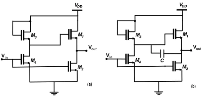
3. PSEUDO-CMOS INVERTER: Third topology is the Pseudo-CMOS inverter as shown in Fig. 4(a). The feature of this topology is that it can replicate the behaviour of the CMOS inverter. When the input is low, M1is on and M2 is off. The output voltage Vout is given by (7).
Vout ≈ VDD− 2Vth (7)
When the input is high, M1is off and M2is on, making Vout ≈ VSS. Two additional TFTs M3 and M4 are added in front of load TFT M1 so that the input signal is inverted to imitate the CMOS inverter behavior. The advantage of this inverter is that it improves the output swing mainly VOL by making M2 and M1 on and off simultaneously. This helps to reduce the static current through M1 and M2 branch, resulting in low power consumption.
4. PSEUDO-CMOS BOOTSTRAPPED INVERTER: By combining the advantages of both pseudo-CMOS and bootstrapped inverters, Pseudo CMOS Bootstrapped in-verter is designed as shown in Fig. 4(b). By incorporating
M2 VDD M1 Vin Vout M4 M3 M2 VDD M1 Vin Vout M4 M3 C (a) ( )(a) (a) (b)
Fig. 4. Circuit schematic formed with (a) Pseudo-CMOS configuration and (b) Pseudo-CMOS Bootstrapped configuration
Pseudo-CMOS topology, it can replicate the behavior of CMOS inverter by adding two additional TFTs (M3and M4) in front of load TFT (M1) which helps to improve VOL by reducing the static current through the driving TFT (M2). The bootstrapped capacitor helps to improve VOH. When input goes from low to high, M1 is turned off due to inverted gate signal while M2 is turned on. This will connect the output node to VSS ≈ VOL ≈ 0. When input goes from high to low, M1is turned on and M2 is turned off. At the same time, output voltage also rises, pulling up the gate voltage of M1by bootstrapping through C. The bootstrapped high gate voltage at M1 can set VOH close to VDD. It keeps the advantages of both (Pseudo-CMOS and Capacitive BS) which means VOH ≈ VDD and VOL ≈ 0. Almost full output voltage swing can be obtained by this topology without much compromising with the power and frequency.
IV. RESULTS ANDDISCUSSION
A 5-stage RO is formed by different inverter topolo-gies which are discussed in previous section. As a first step individual inverter performance and simulation outcomes has been presented in Fig. 5 with Diode con-nected, Bootstrapping, Pseudo-CMOS and Bootstrapped Pseudo-CMOS inverters at VDD= 10V. Diode connected inverter does not provide full swing due to design limitations. BS inverter topology provides VOH ≈ VDD but poor VOL. Whereas Pseudo-CMOS provides VOL≈ 0 but poor VOH. By combining both these topologies i.e. Pseudo-CMOS and bootstrapped full swing with respect to Vin can be obtained which is 98% of VDD. This topology can be used for various applications where full swing is needed.
By using all these inverters topologies RO have been designed and simulated in Cadence environment with the power supply rails of 10V, 15V and 20V.
Diode Connected RO: Simulation outcome of RO formed with inverters using diode connected load is shown in Fig. 6. It can be noticed that the output is 55% of VDD. This low peak to peak output swing makes it difficult to operate as clock generator circuits. The driver transistor M1 is much wider than load (Table I) which
TABLE I. DIMENSIONS OFTRANSISTORS FOR THE DIFFERENT INVERTER TOPOLOGIES S.No. Inverter Topology Transistors W(µm) L(µm)
1. Diode connected load M1 20 20
M2 320 20 2. Bootstrapping M1,M2 160 10 M2 20 10 3. Pseudo-CMOS M1,M2 160 10 M3 20 10 M4 20 10 4. Pseudo-CMOS Bootstrapped M1,M2 160 10 M3 20 10 M4 20 10
Fig. 5. Simulation outcomes of different inverter topologies with power supply of 10 V, (a) Diode connected load inverter, (b) Capacitive BS load inverter, (c) Pseudo-CMOS inverter, (d) Pseudo-CMOS BS inverter
leads to large parasitic capacitance in turn limiting the frequency of oscillations.
Fig. 6. Simulation outcome of RO formed with diode connected load
Capacitive Bootstrapping RO:Fig. 7 shows the out-put response of capacitive bootstrapping RO. It can be inferred from the figure that the output is 82% of VDD i.e. provides better swing than diode connected RO. In this, capacitance C is in the same order as Cgs of transistor which makes it operate at high frequency in the range of MHz. The drawback with this topology is poor VOL. To nullify this drawback value of C should be increased which in turn increases the output swing but decreases the frequency of oscillations.
Fig. 7. Simulation outcome of RO formed with capacitive BS load
Pseudo-CMOS RO: Fig. 8 shows the output charac-teristics of Pseudo-CMOS RO. From the figure it can be noticed that VOH is highly compromised due to Vth drop in each stage. However VOLis improved, reaching closer to VSS as it imitates the CMOS inverter behaviour as described before.
Fig. 8. Simulation outcome of RO Pseudo-CMOS inverter topology
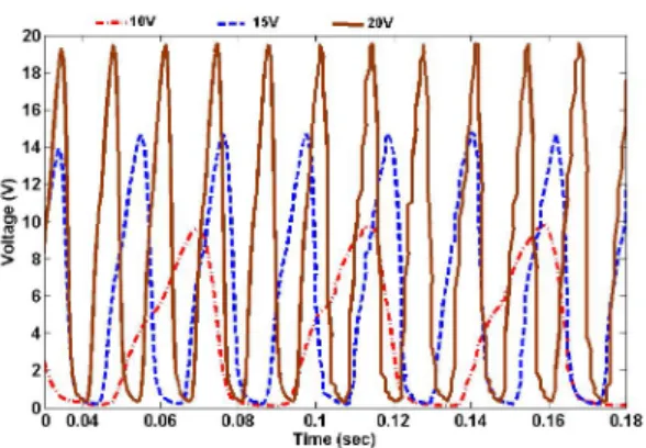
Pseudo-CMOS Bootstrapped RO: Fig. 9 shows the output characteristics of Pseudo-CMOS Bootstrapped RO. By the combination of both the topologies the VOH and VOLof the circuit is improved i.e. VOH ≈ VDDand VOL ≈ VSS, so that peak to peak voltage swing can be improved. The output voltage swing with this topology is 95% of VDD.
Fig. 9. Simulation outcome of RO formed with Pseudo-CMOS BS inverter topology
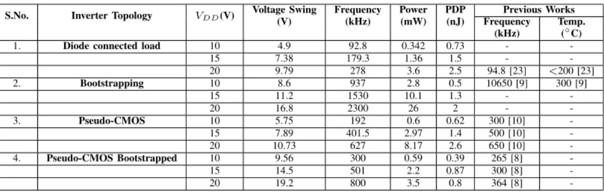
Table II presents the performance matrix of vari-ous ROs with a-IGZO TFTs that are implemented and simulated in this work. Values reported in literature are also included for comparison. It can be seen that bootstrapping RO provides high frequency of operation in the order of MHz with improved figure of merit or PDP (Power Delay Product) compared to other RO topologies. Whereas, Pseudo-CMOS can provide low power consumption with respect to other topologies. The advantages of both these topologies are noticed in Pseudo-CMOS bootstrapped RO which provides high voltage swing peak-to-peak (VP P) with reasonable fig-ure of merit or PDP implemented under same condi-tions. In addition, the performance of ROs in terms of frequency of operation and annealing temperature are compared with the state of art. Since all the simulations are carried out under similar conditions, the user can choose the topology based on the given application. For high frequency of operation-capacitive bootstrapping technique can be used, for low power applications-Pseudo-CMOS can be used and for high voltage swing-the combination of both i.e. Pseudo-CMOS bootstrapped can be used.
V. CONCLUSIONS
This paper presents a comparitive study of various ring oscillators when they are implemented with differ-ent inverter topologies using IGZO TFTs under similar conditions. It can be inferred, for high frequency of operation capacitive BS can be preferred, for low power Pseudo-CMOS topology can be used and if the par-ticular application demands full swing, Pseudo-CMOS Bootstrapping circuit can be used without much com-promising with the figure of merit. These will provide the designer a clear insight of the topology which they can use for a particular application. These on-chip clock generators find potential applications in flexible large area systems such as smart packaging and biomedical wearable electronics.
ACKNOWLEDGMENT
This work is supported by early career research grant with project ref. ECR/2017/000931. This work is par-tially funded by FEDER funds through the COMPETE 2020 Program and National Funds through FCT Por-tuguese Foundation for Science and Technology under project number POCI-01-0145-FEDER-007688, Refer-ence UID/CTM/50025. This work also received fund-ing from the European Community H2020 program under grant agreements No. 716510 (ERC-2016-STG TREND), No. 644631 (Roll-Out) and No. 692373 (BET-EU). This work is partially funded by FEDER funds through the COMPETE 2020 Program and National Funds through FCT Portuguese Foundation for Science and Technology under project number POCI-01-0145-FEDER-007688, Reference UID/CTM/50025 and the doctoral grant research number SFRH/BD/122286/2016.
REFERENCES
[1] C. Hwang, S. Bibyk, M. Ismail, and B. Lohiser, “A very low frequency, micropower, low voltage cmos oscillator for noncar-diac pacemakers,” IEEE Transactions on Circuits and Systems I: Fundamental Theory and Applications, vol. 42, no. 11, pp. 962–966, 1995.
[2] K. Nomura, H. Ohta, A. Takagi, T. Kamiya, M. Hirano, and H. Hosono, “Room-temperature fabrication of transparent flexi-ble thin-film transistors using amorphous oxide semiconductors,” Nature, vol. 432, no. 7016, pp. 488–492, 2004.
[3] G. Bahubalindruni, V. G. Tavares, P. Barquinha, C. Duarte, R. Martins, E. Fortunato, and P. G. de Oliveira, “Basic ana-log circuits with a-gizo thin-film transistors: Modeling and simulation,” in Synthesis, Modeling, Analysis and Simulation Methods and Applications to Circuit Design (SMACD), 2012 International Conference on. IEEE, 2012, pp. 261–264. [4] K. Myny and S. Steudel, “16.6 flexible thin-film nfc transponder
chip exhibiting data rates compatible to iso nfc standards using self-aligned metal-oxide tfts,” in Solid-State Circuits Conference (ISSCC), 2016 IEEE International. IEEE, 2016, pp. 298–299. [5] B.-D. Yang, J.-M. Oh, H.-J. Kang, S.-H. Park, C.-S. Hwang, M. K. Ryu, and J.-E. Pi, “A transparent logic circuit for rfid tag in a-igzo tft technology,” ETRI Journal, vol. 35, no. 4, pp. 610–616, 2013.
[6] T.-C. Huang, K. Fukuda, C.-M. Lo, Y.-H. Yeh, T. Sekitani, T. Someya, and K.-T. Cheng, “Pseudo-cmos: A design style for low-cost and robust flexible electronics,” IEEE Transactions on Electron Devices, vol. 58, no. 1, pp. 141–150, 2011.
[7] D. H. Kang, I. Kang, S. H. Ryu, and J. Jang, “Self-aligned coplanar a-igzo tfts and application to high-speed circuits,” IEEE Electron Device Letters, vol. 32, no. 10, pp. 1385–1387, 2011. [8] Y. Chen, D. Geng, T. Lin, M. Mativenga, and J. Jang, “Full-swing clock generating circuits on plastic using a-igzo dual-gate tfts with pseudo-cmos and bootstrapping,” IEEE Electron Device Letters, vol. 37, no. 7, pp. 882–885, 2016.
[9] H. Yin, S. Kim, C. J. Kim, J. C. Park, I. Song, S.-W. Kim, S.-H. Lee, and Y. Park, “Bootstrapped ring oscillator with propagation delay time below 1.0 nsec/stage by standard 0.5 µm bottom-gate amorphous ga 2 o 3-in 2 o 3-zno tft technology,” in Electron Devices Meeting, 2008. IEDM 2008. IEEE International. IEEE, 2008, pp. 1–4.
[10] J.-D. Wu, F. Zhan, L. Zhou, W.-J. Wu, M. Xu, L. Wang, R.-H. Yao, J.-B. Peng, and M. Chan, “A low-power ring oscillator using pull-up control scheme integrated by metal–oxide tfts,” IEEE Transactions on Electron Devices, vol. 64, no. 12, pp. 4946–4951, 2017.
TABLE II. PERFORMANCEMATRICES OFVARIOUSROS WITH A-IGZOFOR FLEXIBLE ELECTRONICS S.No. Inverter Topology VDD(V)
Voltage Swing (V) Frequency (kHz) Power (mW) PDP (nJ) Previous Works Frequency (kHz) Temp. (◦C)
1. Diode connected load 10 4.9 92.8 0.342 0.73 -
-15 7.38 179.3 1.36 1.5 - -20 9.79 278 3.6 2.5 94.8 [23] <200 [23] 2. Bootstrapping 10 8.6 937 2.8 0.5 10650 [9] 300 [9] 15 11.2 1530 10.1 1.3 - -20 16.8 2300 26 2 - -3. Pseudo-CMOS 10 5.75 192 0.6 0.62 300 [10] -15 7.89 401.5 2.97 1.4 500 [10] -20 10.73 627 8.17 2.6 650 [10] -4. Pseudo-CMOS Bootstrapped 10 9.56 300 0.59 0.39 265 [8] -15 14.5 501 2.2 0.87 300 [8] -20 19.2 800 3.5 0.8 364 [8]
-[11] M. J. Seok, M. Mativenga, D. Geng, and J. Jang, “Achieving high performance oxide tft-based inverters by use of dual-gate configurations with floating and biased secondary gates,” IEEE Transactions on Electron Devices, vol. 60, no. 11, pp. 3787– 3793, 2013.
[12] S. De Vusser, J. Genoe, and P. Heremans, “Influence of transistor parameters on the noise margin of organic digital circuits,” IEEE Transactions on Electron Devices, vol. 53, no. 4, pp. 601–610, 2006.
[13] Y. Cai, Z. Cheng, W. C. W. Tang, K. M. Lau, and K. J. Chen, “Monolithically integrated enhancement/depletion-mode algan/gan hemt inverters and ring oscillators using hboxcf 4 plasma treatment,” IEEE transactions on electron devices, vol. 53, no. 9, pp. 2223–2230, 2006.
[14] A. Mahajan, G. Cueva, M. Arafa, P. Fay, and I. Adesida, “Fabri-cation and characterization of an inalas/ingaas/inp ring oscillator using integrated enhancement-and depletion-mode high-electron mobility transistors,” IEEE Electron Device Letters, vol. 18, no. 8, pp. 391–393, 1997.
[15] K. Myny, S. Steudel, S. Smout, P. Vicca, F. Furthner, B. van der Putten, A. K. Tripathi, G. H. Gelinck, J. Genoe, W. Dehaene et al., “Organic rfid transponder chip with data rate compatible with electronic product coding,” Organic Electronics, vol. 11, no. 7, pp. 1176–1179, 2010.
[16] I. Nausieda, K. Ryu, D. He, A. Akinwande, V. Bulovi´c, and C. Sodini, “Dual threshold voltage integrated organic technol-ogy for ultralow-power circuits,” in Electron Devices Meeting (IEDM), 2009 IEEE International. IEEE, 2009, pp. 1–4. [17] R. Martins, A. Nathan, R. Barros, L. Pereira, P. Barquinha,
N. Correia, R. Costa, A. Ahnood, I. Ferreira, and E. Fortunato, “Complementary metal oxide semiconductor technology with and on paper,” Advanced Materials, vol. 23, no. 39, pp. 4491– 4496, 2011.
[18] K. Nomura, T. Kamiya, and H. Hosono, “Ambipolar oxide thin-film transistor,” Advanced Materials, vol. 23, no. 30, pp. 3431– 3434, 2011.
[19] H. Chen, Y. Cao, J. Zhang, and C. Zhou, “Large-scale com-plementary macroelectronics using hybrid integration of carbon nanotubes and igzo thin-film transistors,” Nature communica-tions, vol. 5, 2014.
[20] K. Nomura, T. Aoki, K. Nakamura, T. Kamiya, T. Nakan-ishi, T. Hasegawa, M. Kimura, T. Kawase, M. Hirano, and H. Hosono, “Three-dimensionally stacked flexible integrated cir-cuit: Amorphous oxide/polymer hybrid complementary inverter using n-type a-in–ga–zn–o and p-type poly-(9, 9-dioctylfluorene-co-bithiophene) thin-film transistors,” Applied Physics Letters, vol. 96, no. 26, p. 263509, 2010.
[21] J. H. Na, M. Kitamura, and Y. Arakawa, “Organic/inorganic hy-brid complementary circuits based on pentacene and amorphous indium gallium zinc oxide transistors,” Applied Physics Letters, vol. 93, no. 21, p. 213505, 2008.
[22] Y. Chen, D. Geng, M. Mativenga, H. Nam, and J. Jang, “High-speed pseudo-CMOS circuits using bulk accumulation a-IGZO TFTs,” IEEE Electron Device Letters, vol. 36, no. 2, pp. 153– 155, 2015.
[23] M. Mativenga, M. H. Choi, J. W. Choi, and J. Jang, “Trans-parent flexible circuits based on amorphous-indium–gallium– zinc–oxide thin-film transistors,” IEEE Electron Device Letters, vol. 32, no. 2, pp. 170–172, 2011.
[24] M. Ofuji, K. Abe, H. Shimizu, N. Kaji, R. Hayashi, M. Sano, H. Kumomi, K. Nomura, T. Kamiya, and H. Hosono, “Fast thin-film transistor circuits based on amorphous oxide semiconduc-tor,” IEEE Electron Device Letters, vol. 28, no. 4, pp. 273–275, 2007.
[25] P. G. Bahubalindruni, V. G. Tavares, P. Barquinha, C. Duarte, N. Cardoso, P. G. de Oliveira, R. Martins, and E. Fortunato, “a-gizo tft neural modeling, circuit simulation and validation,” Solid-State Electronics, vol. 105, pp. 30–36, 2015.
[26] P. Bahubalindrun, V. Tavares, P. Barquinha, P. G. De Oliveira, R. Martins, and E. Fortunato, “InGaZnO TFT behavioral model for IC design,” Analog Integrated Circuits and Signal Process-ing, vol. 87, no. 1, pp. 73–80, 2016.