824 Brazilian Journal of Physics, vol. 36, no. 3B, September, 2006
Electron Mobility Study of Hot-Wall CVD GaN and InN Nanowires
Elena Cimpoiasu, Eric Stern, Guosheng Cheng, Ryan Munden, Aric Sanders, and Mark A. Reed Departments of Electrical Engineering, Biomedical Engineering,
and Applied Physics, Yale University, P.O. Box 208284, New Haven, CT 06520, USA
Received on 5 December, 2005
A review of the dependence of the electron mobility on the free carrier concentration for gallium nitride and indium nitride nanowires grown using hot-wall chemical vapour deposition is presented. Gallium nitride nanowires exhibit mobilities of 100 cm2/Vs to below 1 cm2/Vs for carrier concentrations of 1019to 1020cm−3. Theoretical estimations and annealing experiments indicate that the nanowires are heavily compensated. Indium nitride nanowires also exhibit high carrier concentrations, of the order of 1020 to 1022 cm−3. For both types of nanowires, mobility decreases with increasing carrier concentration, consistent with transport limited by impurity scattering.
Keywords: GaN; InN; Nanowires; Electron transport
I. INTRODUCTION
The group III-nitrides and their alloys represent a promis-ing system for semiconductpromis-ing device applications, especially for photonic devices, because they are direct band gap semi-conductors with potential light emission from ultraviolet to infrared. Growth of GaN and InN nanowires was reported by a number of groups employing mainly catalyzed vapor-liquid-solid (VLS) or catalyst-free vapor-solid (VS) growths ([1], [2] and References therein). One simple, economical and very successful method to grow both types of nanowires is us-ing hot-wall chemical vapor deposition. Understandus-ing the electronic properties of the as-grown nanowires is a crucial step towards their implementation in useful devices. Here we summarize the electric properties of a large number of devices (field-effect transistors) that we built with nanowires grown using this simple process. Both indium nitride and gallium ni-tride nanowires exhibit high carrier concentrations, with mo-bilities limited by impurity scattering. In particular, the gal-lium nitride nanowires appear to grow heavily compensated, as inferred from our theoretical estimates and annealing ex-periments.
II. EXPERIMENTAL AND RESULTS
Gallium nitride and indium nitride nanowires were grown using a hot-wall chemical vapor deposition (CVD) system described elsewhere [3]. The GaN NWs were synthesized via metal-catalyzed (Ni or Fe) VLS growth on alumina or oxidized silicon substrates. This process involved solid gal-lium source (either metallic Ga or metallic Ga combined with Ga2O3 powder), heated to temperatures between 800 and
1100 ˚ C, in ammonia flowing at 2 sccm to 100 sccm. This process consistently yielded nanowires with similar structural and electrical properties for similar growth parameters, of high crystalline quality.
Indium nitride nanowires were grown using a catalyst-free method, assumed to follow the vapor-solid route. Growth sources were a mixture of indium and indium oxide, heated to 700 ˚ C in ammonia flowing at 100 sccm. This growth process
yielded very large amounts of nanowires on the wall of the furnace.
The as-grown nanowires were subsequently suspended in solution and dispersed on silicon wafers covered with 200 nm oxide. Optical lithography was chosen to fabricate the dis-persed wires in field-effect transistor devices as test probes of the electrical properties. The advantage of using optical lithography as opposed to electron beam lithography is that it allows parallel processing of a large number of NWs and pro-vides a blind testing of their electronic properties. In this way a large number of nanowires were electrically investigated and the effects of different growth parameters on these properties were successfully singled out [3].
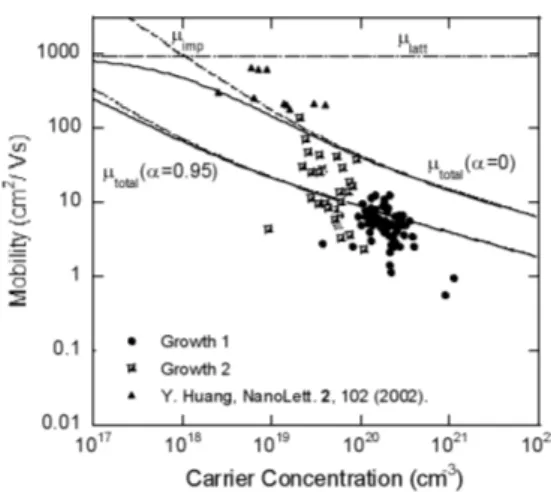
Figure 1 shows the dependence of the extracted mobilities µas a function of the free carrier concentrationn. The plot in-cludes three sets of data: the filled circles represent results of a non-optimized typical growth (Growth 1), the squares repre-sent results from best, optimized growth (Growth 2), and the triangles are the best reported results for GaN NWs, grown us-ing a laser-assisted VLS process [4]. The growth parameters of Growth 1 and Growth 2 are listed in Table 1.
TABLE I: Growth Parameters for GaN NWs
Growth1 Growth2 Temperature ( ˚ C) 800 950 Ammonia Flow (sccm) 100 2 Substrate Si/SiO2 Si/SiO2 Gallium Source Ga+Ga2O3 Ga+Ga2O3 Pressure 1 atm 1 atm Metal Catalyst Ni Fe
Elena Cimpoiasu et al. 825
FIG. 1: Mobility versus free carrier concentration for GaN nanowires from Growth 1, Growth 2, and from Ref. [4]. Continuous black lines represent theoretically estimated mobility for compensation levelsα =0 and 0.95.
µimp=
64√πε2(2kT)3/2 Nie3
√
m∗ {ln[1+ ( 12πεkT
e2N1/3
i
)2]}−1 (1)
Here ε=8.9ε0 [7] is the semiconductor permittivity, k is
the Boltzmann’s constant, T is the temperature in Kelvin, m∗=0.2m0 [7]) is the effective mass of electrons, andNi= ND+NAis the density of ionized impurities, equal with the sum between ionized donor and acceptor impurities.
Ionized impurity scattering is not the only scattering process for the free carriers. Other mechanisms include phonon (acoustic and optical) scattering, scattering at stack-ing faults and point defects. However, these mechanisms do not exhibit a relevantndependence and we account for their effect using a fixed mobility component, µlatt [8]. Here we chooseµlatt = 900 cm2/Vs to account for the high values of mobility from Reference [4]. We should note that the exact value ofµlattis not particularly relevant for these high carrier concentrations (1019-1021cm−3), as seen from Fig. 1.
The total mobility µtotal is then calculated using Matthiesen’s rule:
1 µtotal
= 1 µimp
+ 1 µlatt
(2)
Figure 1 shows the estimated total mobility for uncompen-sated (α=0) and heavily compensated (α=0.95) material
(con-tinuous black line,α=NA/ND). One can notice that Growth
1 exhibits heavy levels of compensation, while the optimized one lies in between the uncompensated and heavily compen-sated lines. This indicates that the observed reduction in the carrier concentration is due to a substantial decrease of the donor impurities/defects sites.
FIG. 2: Mobility versus free carrier concentration for GaN nanowires from as-grown and ammonia or forming gas annealed samples (with growth parameters similar with Growth 1, except Tgrowth=900 ˚ C ).
Continuous black line represents theoretically estimated mobility for α=0.95.
In order to understand more of the origin of these high car-rier concentrations, we performed annealing experiments of samples with growth parameters similar to the Growth 1 and Growth 2. If the source of the low mobility/high carrier con-centration are nitrogen vacancies and oxygen impurities (as it is wildly speculated in the literature), annealing in conditions that would favor reduction of their concentration would result in improved electrical properties (lown, highµ). It is con-ceivable that annealing in ammonia at high temperature for long periods of time would allow diffusion of nitrogen from decomposed ammonia into the nanowires to fill in the nitro-gen vacancies. By the same token, annealing in forming gas would extract some oxygen impurities, therefore reduce the concentration of one other important source ofn-type behav-ior.
regard-826 Brazilian Journal of Physics, vol. 36, no. 3B, September, 2006
FIG. 3: Mobility versus free carrier concentration for GaN nanowires from as-grown and ammonia-annealed samples from Growth 1. Con-tinuous black lines represent theoretically estimated mobility for compensation levelsα=0 and 0.95.
ing the cause of decreasedn, especially at these high carrier concentration levels. Indeed, because of the small slope of the µ-Ni dependence and the high device-to-device fluctuations, it is hard to distinguish between reduction ofndue to the de-crease of the donor sites (which should also inde-crease mobility) or reduction ofn due to increase in the compensation levels (accompanied by a decrease of mobility).
In order to confirm the role of ammnonia anneal on nitrogen vacancies/impurities levels, we performed a second anneal us-ing samples from the optimized growth (Growth 2). This re-sult is shown in Fig. 3, where the filled circles represent the properties of the as-grown sample, while the centered squares represent the properties of the 4 h NH3-annealed sample. It is
evident that the annealed sample has significantly lower car-rier concentration and mobility, indicative of increased lev-els of compensation. Thus, we conclude that the reduction of the carrier concentration after annealing in ammonia is due to compensation effects. Although data does not allow con-cluding remarks about the source of compensation, we can speculate that hydrogen (from the decomposed ammonia) and probably carbon might diffuse inside the nanowires and par-ticipate in donor compensation [9].
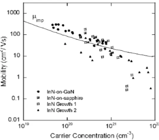
Theoretical estimates similar to above were performed for the electronic properties of InN nanowires. Figure 4 shows the mobility dependence on carrier concentration for two sim-ilar InN NWs growths, together with published results on epitaxially-grown InN grown on GaN [11-14] and sapphire substrates [11] . The solid curve is the calculated impu-rity scattering mobility using Eq. 1, where ε=15.3ε0 and m∗=0.11m0[15]. The nanowires show high carrier
concen-trations, of the order of 1020 to 1022cm−3, but the values of
the mobility line up to the results previously reported for the epitaxially-grown films. The theoretical estimate exhibits a reasonable agreement to the data, with an overestimation of
the reduction in mobility due to impurity scattering. The
ex-FIG. 4: Scatter plot of mobility vs. carrier concentration for two growth-fabrication runs of InN NWs. Data from bulk epitaxially-grown InN on sapphire [11] and GaN [11-14] substrates are included. Continuous black line represents theoretically estimated mobility due to ionized impurity scattering (α=0).
perimental points deviate from the theoretical curve fornover 1021cm−3, probably due other competing scattering mecha-nisms at these high concentration levels.
III. CONCLUSION
Gallium nitride and indium nitride were successfully grown using hot-wall chemical vapor deposition (tube furnace) and built into a large number of devices which were used to sta-tistically probe their electronic properties. We found that both types of nanowires exhibit large carrier concentrations, with a decreasing mobility upon increasing free carrier concentra-tions, consistent with transport dominated by impurity scat-tering. In the case of the gallium nitride nanowires, using feedback between the growth parameters and electrical char-acterization, we were successful in decreasing (increasing) the carrier concentration (mobility) by one order of magnitude. Also, simple theoretical estimates and annealing experiments indicate that the gallium nitride nanowires grow heavily com-pensated.
Acknowledgement
Elena Cimpoiasu et al. 827
[1] M. Law, J. Goldberger, and P. Yang, Annu. Rev. Mater. Res.
34, 83 (2004).
[2] G. Cheng, E. Stern, D. Turner-Evans, and M. A. Reed, Appl. Phys. Lett.87, 253103 (2005). .
[3] E. Stern, G. Cheng, E. Cimpoiasu, R. Klie, S. Guthrie, J. Klemic, I. Kretzschmar, E. Steinlauf, D. Turner-Evans, E. Broomfield, J. Hyland, R. Koudelka, T. Boone, M. Young, A. Sanders, R. Munden, T. Lee, D. Routenberg, and M. A. Reed, Nanotechnology16, 2941 (2005).
[4] Y. Huang, X. Duang, Y. Cui, and C.M. Lieber, Nano Letters2, 102 (2002).
[5] S.M. Sze, Physics of Semiconductor Devices, John Wiley & Sons New York, pg. 28, 1985.
[6] E. Conwell and V.F. Weisskopf, Phys. Rev.77, 388 (1950). [7] I.M. Abdel-Motaleb and R.Y. Korotkov, J. Appl. Phys. 97,
093715 (2005).
[8] N. G. Weimann and L. F. Eastman, J.Appl. Phys. 83, 3656
(1998).
[9] We should mention, however, that calculations for the diffusion barrier of hydrogen predict∼3.4 eV, a reason for which hydro-gen in not very mobile and large amounts of hydrohydro-gen are not readily incorporated during growth [10].
[10] J. Neugebauer and C.G. Van de Walle, Appl. Phys. Lett.68, 1829 (1996).
[11] A. Yamamoto, T. Shin-ya, T. Sugiura, and A. Hashimoto, J. Cryst. Growth189/190, 461 (1998).
[12] C. R. Abernathy, S. J. Pearton, F. Ren, and P. W. Wisk, J. Vac. Sci Technol. B11, 179 (1993).
[13] W. A. Bryden, S. A. Ecelberger, and T. J. Kistenmacher, Appl. Phys. Lett.64, 2864 (1994).
[14] Y. Sato and S. Sato, J. Cryst. Growth146, 262 (1994). [15] V.W.L. Chin, T.L. Tansley, and T. Osotchan, J. Appl. Phys.75,