ISSN 1546-9239
© 2007 Science Publications
Corresponding Author: Zied Gafsi, Microelectronic and Instrumentation Laboratory (µEi), Physics Department, Science Faculty of Monastir, Rue de l'environnement, Monastir 5000, Tunisia, Tel: 0021698474750 or 0021673500274, Fax: 0021673500278
A New Efficient-Silicon Area MDAC Synapse
Zied Gafsi, Nejib Hassen, Mongia Mhiri and Kamel Besbes
Microelectronic and Instrumentation Laboratory (µEI), Monastir University, Tunisia
Abstract: Using the binary representation ∑iDi2i in the Multiplier digital to analog converter (MDAC)
synapse designs have crucial drawbacks. Silicon area of transistors, constituting the MDAC circuit, increases exponentially according to the number of bits. This latter is generated by geometric progression of common ratio equal to 2. To reduce this exponential increase to a linear growth, a new synapse named Arithmetic MDAC (AMDAC) is designed. It functions with a new representation based on arithmetic progressions. Using the AMS CMOS 0.35µm technology the silicon area is reduced by a factor of 40%.
Key words: MDAC, binary representation, efficient silicon area
INTRODUCTION
Neural network are very suitable to resolve problems where conventional resolution methods fall
[1-3]
. Synapses are the common bloc in neural network. It functions as multipliers. Their roles are to weight neural inputs by synaptic weights. Several research aims to implement synapses. Some use numeric implementation whereas others use analogue circuit. Each of these method implementations has its own advantages and drawbacks. Numeric multipliers are very suitable for applications that need high accuracy and precision results[4]. Unfortunately it occupies a considerable silicon area. Analogue synapses are efficient-silicon area and are able to operate at high frequency. However synaptic weights are badly saved in their analogue form[5-13]. To combine the advantages of these last implementation methods, a mixed implementation technique provides best performances[14-22].
A mixed synapse named multiplier digital-to-analogue converter (MDAC) is a multiplier bloc that multiplies an analogue reference by a binary coded synaptic weight. This last is converted by a digital to analogue converter (DAC) to an analogue size, multiplied by the analogue reference and the result is routed to the output of the synapse. Current steering MDAC is the aim of this work for its capability to drive considerable charges at the output of synapses.
Several codes are used to represent the digital synaptic weights[14,15,17,20-22]. The most popular are the thermometer code and the weighted binary code. The advantage of the first cited one is its low glitches.
W0
W1
Wi
Wp-1
X0
X1
Xi
Xp-1
Neuron
Y S(.)
+
…
…
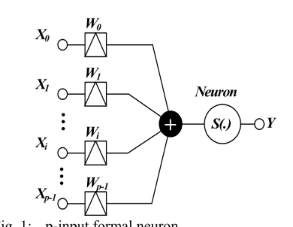
Fig. 1: p-input formal neuron
However to represent N-bits synaptic weight, 2N-1 identical current sources are needed. To represent the same weight using binary weighted representation, N current sources, which values follow a geometric progression, are used. The use drawback of such representation is the exponential increase of the current source magnitudes. Face to this problem the design of a new MDAC synapse architecture, called AMDAC, using arithmetic progression will be presented.
Multiplication operation: Neural network are defined
as the nonlinear function of weighted sum of signals. The p-inputs of neuron, X0, X1… Xp-1 shown in Fig. 1,
are multiplied by the p-synaptic weights, W0, W1…, Wp-1.
p 1
i i i 0
Y S X W
−
=
=
∑
(1)From the previous equation, multiplication operation of XiWi and the addition ΣiXiWi are the two
arithmetic operation performed by the neuron. The implementation of the addition is easy if outputs of the synapses are currents. It is performed when synapse outputs are connected together according to kirchhoff law (KCL). The difficulty lies in the implementation of the multiplication operation.
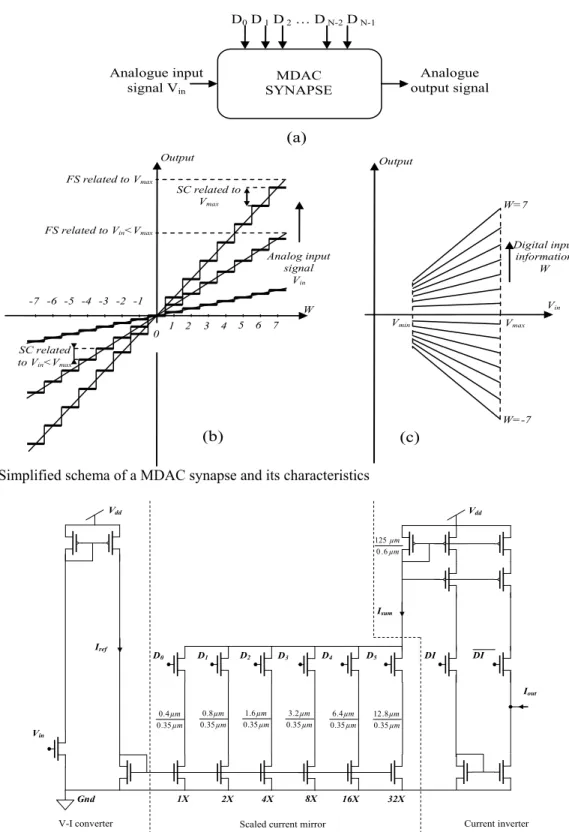
The MDAC synapse shown in Fig. 2a is a bloc diagram that multiplies the analog voltage Vin by the
binary coded synaptic weight DN-1DN-2…D2D1D0. The
transfer characteristics of MDAC synapse, shown in Fig. 2b and 2c, take two forms. On one hand, when Iout
current is plotted according to the analog voltage Vin,
characteristics are straight lines which its slopes vary linearly. On the other hand, Iout is a staircase shaped
curves when it is plotted according to synaptic weights. From these curves integral nonlinearity error (INL) and differential nonlinearity error (DNL) are concluded. INL is an error characterization between the real staircase shaped curve and the ideal characteristic generally obtained by linear approximation of the real curve.
DNL error give a measure of how well an MDAC can generate uniform smallest analog change LSB. Thus binary synaptic inputs DN-1DN-2…D2D1D0 and
analog input voltage are combined by the multiplication operation:
(
)
out N 1 N 2 2 1 0 in
I = ⋅K C D −, D − ,", D , D , D ⋅V (2)
Where Iout is the output current of the synapse, K is a
constant, Vin is the analog input voltage and C(DN-1,D N-2,…D2,D1,D0) is to binary-to-decimal conversion law.
For the weighted binary representation C(DN-1,D N-2,…D2,D1,D0) is expressed by:
(
)
N 1 iN 1 N 2 2 1 0 i
i 0
C D , D , , D , D , D 2 D
−
− −
=
=
∑
" (3)
Binary weighted current steering MDAC
MDAC circuit: The 6-bits MDAC synapse, shown in
Fig. 3 is composed of:
* An input circuit converting the analog input voltage Vin to a proportional current Iref.
* A series of scaled current mirror so that a mirror produces twice the current produced by the preceding one. Each of the stored bits D0 to D6
controls a switch transistor.
* An output circuit inverting the sign of the current I issued from current mirrors. The sign circuit
determines the direction of the output current, i.e. DI=0 creates a positive (excitatory) synaptic current and DI=1 sets a negative (inhibitory) synaptic current.
* The total output current resulting from the scaled current mirrors is expressed by:
5 i
sum i
i 0 dd
V
I I
V
=
=
∑
(4)Where Ii (i=0…5) is the flowing current in the current
mirror i and Vi is the gate voltage controlling the
current Ii. Vi takes only either of values Vdd or zero. It is
then expressed according to the binary value Di by:
i i dd
V =D V⋅ (5)
In the case of Di=0 then Vi=0. In the other case,
when Di=1 then Vi=Vdd. As the size ratio of different
current mirrors follow a geometric progression having the common ratio equal to 2, the current Ii is done by:
i
i 0
I =2 I (6)
Substituting the equations 5 and 6 in 4 the expression of Isum is done by:
5 i
sum 0 i
i 0
I I 2 D
=
= ⋅
∑
(7)From the previous equation, the weighted binary to decimal conversion law is shown. Furthermore multiplication operation is shown between the analog input current and the binary to decimal conversion law. Finally, considering the sign bit DI, Iout is expressed by:
( )
5DI i
sum 0 i
i 0
I I 1 2 D
=
= ⋅ −
∑
(8)Simulation results of MDAC: Several simulations are
carried out using 0.35µm CMOS AMS process. Figure 4 shows good linearity of the V-I converter between input analog voltage Vin and the converted current Iin
from Vin=2volt. The linearity of the V-I converter have
380
0 1 2 3 4 5 6 7
SC related to Vmax
-1 -2 -3 -4 -5 -6
Output
Analog input signal
Vin
W=7
W
Digital input information
W
W=-7
Vmin Vmax
Output
FS related to Vmax
FS related to Vin<Vmax
Vin
-7
SC related to Vin<Vmax
(b) (c)
Analogue input signal Vin
D0 D 1 D 2 … D N-2 D N-1
Analogue output signal MDAC
SYNAPSE
(a)
Fig. 2: Simplified schema of a MDAC synapse and its characteristics
DI DI
Vin
Vdd
Gnd 32X
D0 D1 D2 D4 D5
µm µm
35 . 0
4 . 0
2X 4X 16X
Vdd
Iout
Isum
Iref
V-I converter Scaled current mirror Current inverter
D3
µm µm
35 . 0 8 . 0
µm µm
35 . 0 6 . 1
µm µm
35 . 0
2 . 3
µm µm
35 . 0 4 . 6
µm µm
35 . 0 8 . 12
1X 8X
µm µm
6 . 0 125
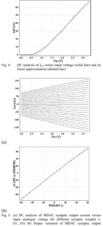
Fig. 4: DC analysis of Iref versus input voltage (solid line) and its
linear approximation (dashed line)
(a)
(b)
Fig. 5: (a) DC analysis of MDAC synaptic output current versus input analogue voltage for different synaptic weights (-63…63) (b) Slopes variation of MDAC synaptic output current (dotted curve) and its linear approximation (solid curve)
Arithmetic progression based MDAC: AMDAC From geometric to arithmetic progression:
The MDAC, circuit presented in the
Fig. 6: MDAC Synapse output current versus synaptic weights
(±63 level) for various input voltages Vin (2.0, 2.1, 2.2…
3.3V)
Fig. 7: DNL and INL error of weight binary MDAC
382
DI DI
6X D1 D2 D4 D5
2X 3X 5X
Vdd Iout Isum Vin Vdd Gnd Iref
V-I converter Scaled current mirror Current inverter
D3 µm µm 35 . 0 8 . 0 µm µm 35 . 0 9 . 0 µm µm 35 . 0 0 . 1 µm µm 35 . 0 1 . 1 µm µm 35 . 0 2 . 1 D0 µm µm 35 . 0 7 . 0
1X 4X
µm . µm 6 0 42 DI µm . µm . 6 0 1 3 Vdd
DI DC
Correction circuit D6 µm . µm . 35 0 3 1 7X D7 µm . µm . 35 0 4 1 8X µm . µm . 35 0 6 0
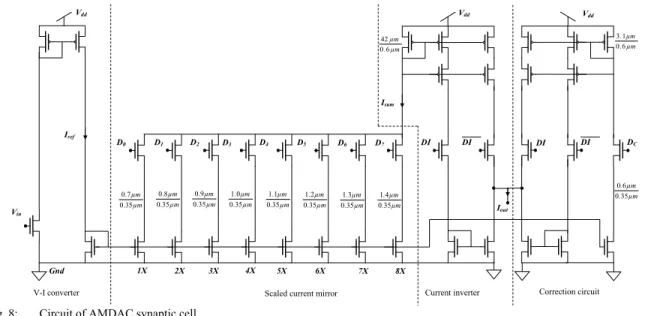
Fig. 8: Circuit of AMDAC synaptic cell
Table 1: 9-bit A2 unsigned binary representation based on arithmetic progression
D7 D6 D5 D4 D3 D2 D1 D0 W
0 0 0 0 0 0 0 0 0 0 0 0 0 0 0 0 1 1 0 0 0 0 0 0 1 0 2 0 0 0 0 0 1 0 0 3 0 0 0 0 1 0 0 0 4 0 0 0 1 0 0 0 0 5 0 0 1 0 0 0 0 0 6
0 1 0 0 0 0 0 0 7
1 0 0 0 0 0 0 0 8
0 0 0 0 0 0 1 1 9
0 0 0 0 0 1 0 1 10 0 0 0 0 1 0 0 1 11 0 0 0 1 0 0 0 1 12 0 0 1 0 0 0 0 1 13
0 1 0 0 0 0 0 1 14
1 0 0 0 0 0 0 1 15 1 0 0 0 0 0 1 0 16 1 0 0 0 0 1 0 0 17 1 0 0 0 1 0 0 0 18 1 0 0 1 0 0 0 0 19 1 0 1 0 0 0 0 0 20
1 1 0 0 0 0 0 0 21
0 1 0 0 0 0 1 1 22
1 0 0 0 0 0 1 1 23
1 0 0 0 0 1 0 1 24
D7 D6 D5 D4 D3 D2 D1 D0 W
1 0 0 0 1 0 0 1 25
1 0 0 1 0 0 0 1 26
1 0 1 0 0 0 0 1 27
1 1 0 0 0 0 0 1 28
1 1 0 0 0 0 1 0 29
1 1 0 0 0 1 0 0 30
1 1 0 0 1 0 0 0 31
1 1 0 1 0 0 0 0 32
1 1 1 0 0 0 0 0 33
1 0 0 1 0 0 1 1 34
1 0 1 0 0 0 1 1 35
1 1 0 0 0 0 1 1 36
1 1 0 0 0 1 0 1 37
1 1 0 0 1 0 0 1 38
1 1 0 1 0 0 0 1 39
1 1 1 0 0 0 0 1 40
1 1 1 0 0 0 1 0 41
1 1 1 0 0 1 0 0 42
1 1 1 0 1 0 0 0 43
1 1 1 1 0 0 0 0 44
1 1 0 0 0 1 1 1 45
1 1 0 0 1 0 1 1 46
1 1 0 1 0 0 1 1 47
1 1 1 0 0 0 1 1 48
1 1 1 0 0 1 0 1 49
D7 D6 D5 D4 D3 D2 D1 D0 W
1 1 1 0 1 0 0 1 50
1 1 1 1 0 0 0 1 51
1 1 1 1 0 0 1 0 52
1 1 1 1 0 1 0 0 53
1 1 1 1 1 0 0 0 54
1 1 0 0 1 1 1 1 55
1 1 0 1 0 1 1 1 56
1 1 1 0 0 1 1 1 57
1 1 1 0 1 0 1 1 58
1 1 1 1 0 0 1 1 59
1 1 1 1 0 1 0 1 60
1 1 1 1 1 0 0 1 61
1 1 1 1 1 0 1 0 62
1 1 1 1 1 1 0 0 63
0 1 1 1 1 1 1 1 64 1 0 1 1 1 1 1 1 65
1 1 0 1 1 1 1 1 66
1 1 1 0 1 1 1 1 67
1 1 1 1 0 1 1 1 68
1 1 1 1 1 0 1 1 69
1 1 1 1 1 1 0 1 70
the first term of the geometric progression with which the scaled mirror sizes of the MDAC follow. Consequently, the series of scaled mirror width were:
{
0.4µm, 0.8µm, 1.6µm, 3.2µm, 6.4µm, 12.8µm}
(9)The common ratio of the last geometric progression is equal to 2. To handle the transition of a weighted MDAC state to the following, an increase with the two’s power of manufacturing grid is enough. Furthermore an arithmetic progression can limit the exponential increase of the geometric progression terms. Its common difference (CD) is equal to two’s power of manufacturing grid. Let choose the common difference equal to 0.1µm and the first terms equal to 0.7µm. the eight arithmetic terms are:
0.7µm, 0.8µm, 0.9µm, 1.0µm, 1.1µm, 1.2µm, 1.3µm, 1.4µm
(10)
The Fig. 8 shows the circuit of AMDAC. The V-I converter and the current inverter of the AMDAC are the same that the ones presented in Fig. 3. The scaled mirror sizes follow the arithmetic progression terms of the series-10. Obviously the number representation is not the weighted binary code. A new binary representation based on arithmetic progression named binary arithmetic representation and noted A2 must be established. To represent the first state, 0.7µm-current mirror width is activated. Thus the first number representation is:
2
10
00000001
1
A
=
(11)Where, the 1|10 and 00000001|A2 are respectively the
notations of the decimal value of one and its A2 binary representation. In this last the only one valued bit is at the least significant bit.
The following states are generated by adding each time the common difference CD equal to 0.1µm. This corresponds to shifting the one valued bit to the more significant bits:
10 A 2
10 A 2
10 A 2
10 A 2
10 A 2
10 A 2
10 A 2
2 00000010
3 00000100
4 00001000
5 00010000
6 00100000
7 01000000
8 10000000
= = = = = = =
(12)
The last value, 8|10, corresponds to the activation of
the current mirror having the width equal to 1.4µm. The next value must activate a current mirror width equal to
1.5µm. This last size can be obtained by the activation of the two current mirrors sized W=0.7µm and W=0.8µm. consequently A2 representation of the decimal value 9|10 is:
2
10
00000011
9
A
=
(13)Higher decimal values are also obtained by shifting one valued bits from the less significant bits towards more significant bits. Table 1 shows the complete eight-bit representation. 71 states are noted. A2 representation is redundant because a decimal value can be represented by several A2 binary codes. For example 00011100|A2 and 00101010|A2 activate the same total
current mirror width. In fact, the mirrors widths activated by the code 00011100|A2 are 0.9µm, 1µm and
1.1µm. the total width is then equal to 3µm. the same width can be obtained by the activation of 0.8µm, 1µm and 1.2µm current mirrors. The only forbidden A2 code is 11111111.
Because the first term in the arithmetic series 0.7, 0.8, 0.9…1.4 is not equal to the common difference, a correction bloc must be placed in the circuit represented in Fig.8 to substrate the equivalent of 0.6µm current mirror width.
The Isum current is expressed by: 7
i
sum i C
i 0 dd
V
I I I
V
=
= −
∑
(14)Where, IC is the correction current. For the same length
transistor of the scaled mirror, the ith mirrored current Ii
is then equal to:
0 i
i 0 0
0 0
W i CD
W
I I I
W W
+ ⋅
= = (15)
Where, W0 and CD are respectively the common
difference and the first term of the arithmetic progression and they are equal to CD=0.1µm and W0=0.7µm. substituting equation 5, 15 in 14 and
considering the sign bit DI the current Isum is expressed
by:
( )
DI 7 70
sum i i
i 0 i 0
I
I 1 7 D 6 iD
7 = =
= − − +
∑
∑
(16)The previous equation is a multiplication between the analog current I0/7 and 9-signed-bit A2
representation.
Simulation results of AMDAC: Simulations AMDAC
are done in the same conditions as the weighted MDAC simulations. Figure 9a illustrates linear variations of Iout
384
Table 2: Performance comparison between 7-signed-bit MDAC and 9-signed-bit AMDAC
Synapse State number Maximum full scale INL error DNL error Silicone area
7-signed-bit MDAC 127 166µA 0.7 LSB 0.6 LSB 909 µm2
9-signed-bit AMDAC 143 70µA 0.7 LSB 0.3 LSB 589µm2
(a)
(b)
Fig. 9: (a) DC analysis of AMDAC synaptic output current versus input analogue voltage for different synaptic weights (-63…63) (b) Slopes variation of AMDAC synaptic output current (dotted curve) and its linear approximation (solid curve)
Fig. 10: AMDAC Synapse output current versus synaptic weights (±63 level) for various input voltages Vin (2.0, 2.1, 2.2… 3.3V)
Fig. 11: DNL and INL error of weight binary AMDAC
slope linear variation of the straight line of Fig. 9a. Staircase shaped curves are shown in Fig. 10. From Fig. 11, INL and DNL measures concluded. Maximum INL and DNL error are respectively 0.7 LSB and 0.3 LSB as shown in Fig. 12.
Layout and comparative analysis: Using AMS
38.2 µm
2
3
.8
µ
m
(a)
25.5 µm
2
3
.1
µ
m
(b)
Fig. 12: Layout area of (a) MDAC, (b) A-MDAC
CONCLUSION
In the present work we designed a new multiplier digital-to analog converter based on arithmetic progression called AMDAC. It functions with a new binary representation. We have demonstrated a gain in silicon area by almost of 40% for better resolution compared to classical MDAC.
REFERENCES
1. Linares-Barranco, B., E. Sanchez-Sinencio, Rodriguez and J.L. Huertas, 1993. A CMOS analog adaptive BAM with on-chip learning and weight refreshing. IEEE Tran. Neural Networks, 4: 3.
2. Rossetto, O., C. Jutten, J. Heraut and I. Kerzer, 1989. Analog VLSI Synaptic Matrices as building blocks for neural networks. IEEE Micro, pp: 56-63.
3. Graf, H.P., L.D. Jackel and W.E. Hubbard, 1988. VLSI implementation of a neural network model. IEEE Computer, 21: 41-49.
4. Conti, M., P. Crippa, G. Guaitini, S. Orcioni and C. Turchertti, 1999. An analog CMOS approximate identity neural network with stochastic learning and multilevel weight storage. IEICE Trans. Fundamentals, E82 A: 7. 5. Schmid, A., 2000. VLSI realisation of mixed
analog-digital artificial neural networks dedicated to autonomous systems with on chip learning capability. Thesis No. 2101. Federal Polytechnique School of Lausanne EPFL.
6. Arima, Y., M. Murasaki, T. Yamada, A. Maeda and H. Shinohara, 1992. A refreshable analog VLSI neural network chip with 400 neurons and 40k synapses. IEEE J. Solid-state Circuits, 27: 12.
7. Zornetzer, S., J. Davis, C. Lau and T. McKenna, 1995. An Introduction to Neural and Electronic Network. Academic Press.
8. Kinoshita, S., T. Morie, M. Nagata and A. Iwata, 1999. New non-volatile analog memory circuits using PWM methods. IEICE Trans. Electron, E82-C: 9.
9. Weber, W., S.J. Prange, R. Thewes, E. Wohlarb and A. Luck, 1996. On the application of the neuron MOS transistor principle for modern VLSI design. IEEE Trans. Electron Device, 43: 1700-1708.
10. Shibata, T. and T. Ohmi, 1992. A functional MOS transistor featuring gate level weighted sum and threshold operations. IEEE, Trans. on Elec. Devices, 39: 6.
11. Shibata, T., H. Kosak and T. Ohmi, 1995. A neurone-MOS neural network using self-learning compatible synapses circuits, IEEE JSSC, 30: 8.
12. Diorio, C., P. Hasler, B.A. Minch and C.A. Mead, 1996. A single transistor silicon synapse. IEEE, Trans. Electron Devices, 43: 11.
13. Fujita, O. and Y. Amemiya, 1993. A floating-gate analog memory device for neural networks. IEEE Trans. Electron Device, 40: 11.
14. Djahanshahi, H., A. Ahmadi, G.A. Jullien and W.C. Miller, 1996. Design and VLSI implementation of a unified synapse-neurone architecture. Proc. 6th Great Symp. VLSI, pp: 228-232.
15. Coggins, R., M. Jabri, B. Flower and S. Pickard, 1995. A hybrid analog and digital VLSI neural network for intracardiac morphology classification. IEEE J. Solid-state Circuits, 30: 5.
16. Duong, T., S.P. Eberhardt, M. Tran, T. Daud and A.P. Thakoor, 1989. Learning and optimization with cascaded VLSI neural network building-block chips. Proc. 3rd Ann. Parallel Processing Symp., 1: 257-267. Fullerton, CA, IEEE Orange County Computer Society.
17. Chen, C.H., 1996. Fuzzy Logic and Neural Network Handbook. IEEE Press.
18. Raffel, J.I., 1988. Electronic implementation of neuromorphic systems. Proc. IEEE Custom Integrated Circuits Conf., pp: 10.1.1.
19. Koosh, V.F. and R. Goodman, 2001. VLSI neural network with digital weight and analog multipliers. Proc. IEEE Intl. Symp. Circuit and Systems, Sidney Australia, 2: 233-236.
20. Mirhassani, M., M. Ahmadi and W.C. Miller, 2003. A mixed-signal VLSI neural network with on-chip learning. Proc. 2003 Canadian IEEE Conf. Electrical and Computer Engineering, 1: 591-595.
21. Mirhassani, M., M. Ahmadi and W.C. Miller, 2003. A feed-forward time-multiplexed neural network with mixed-signal neuron-synapse arrays. Proc. Intl. Conference on VLSI, Las Vegas, USA, pp: 339-342. 22. Mirhassani, M., M. Ahmadi and W.C. Miller, 2006. A