Studies of Phosphorus Gaussian Profile Emitter Silicon Solar Cells
N. Stem*, M. Cid**
Laboratório de Microeletrônica, Depto. de Engenharia de Sistemas Eletrônicos Escola Politécnica da Universidade de São Paulo, C.P. 61548
05424-970 São Paulo - SP, Brazil
Received: January 30, 2001; Revised: April 4, 2001
Considering recent modifications on n-type highly doped silicon parameters, an emitter optimi-zation was made based on one-dimensional models with analytical solutions. In order to get good accuracy, a fifth order approximation has been considered. Two kinds of emitters, homogeneous and non-homogeneous, with phosphorus Gaussian profile emitter solar cells were optimized. According to our results: homogeneous emitter solar cells show their maximum efficiencies (η ≅ 21.60−21.74%) with doping levels Νs = 1x10¹⁹ - 5x10¹⁸ (cm-3) and (1.2-2.0) µm emitter thickness range. Non-homogeneous emitter solar cells provide a slightly higher efficiency (η = 21.82-21.92%), with Ns = 1x10²⁰ (cm-3) with 2.0 µm thickness under metal-contacted surface and Ns = 1x10¹⁹ - 5x10¹⁸ (cm-3) with (1.2-2.0) µm thickness range, (sheet resistance range 90-100 Ω/ ) under passivated surface. Although non-homogeneous emitter solar cells have a higher efficiency than homogeneous emitter ones, the required technology is more complex and their overall interest for practical applications is questionable.
Keywords:solar cell efficiencies-1, homogeneous emitter-2, non-homogeneous emitter-3, Gaussian profile-4
1. Introduction
In order to improve solar cell efficiencies, several theo-retical optimizations of emitter region have been proposed throughout the years. In the eighties a breakthrough oc-curred in the emitter design philosophy aimed to the devel-opment of efficient silicon solar cells1. It was shown that the best emitters should be thick and moderately doped. According to A. Cuevas and M. Balbuena2, solar cells with homogeneous emitters with Ns = 1x10¹⁹ - 5x10¹⁸ (cm-3) and thickness of 1.0-2.0 (µm) are the best ones. In 1990, based on these works, A. Aberle et al. optimized LDD (locally deep diffused) and homogeneous emitters, getting the con-clusion that LDD emitters are better than homogeneous ones3. Despite the required technology to process these emitters are complex, non-homogeneous emitters has still been adopted in research laboratories, and they are found in the solar cells with record efficiencies. However a ques-tion must be asked: are non-homogeneous emitters signifi-cantly better? Moreover, recent modifications of highly
doped n-type parameters made new theoretical optimiza-tions of emitters imperative. Therefore, this work has two important motivations: comparison between the two kinds of emitters and the necessity of optimizing emitters consid-ering updated parameters4. Theoretical models with ana-lytical solutions have been used to study n+ emitter region5,6. Admitting a Gaussian profile, two kinds of emit-ters, homogeneous and non-homogeneous, were optimized and compared considering different kinds of surfaces, emit-ter doping levels and thicknesses. In order to calculate theoretical solar cell efficiency, a complete n+pp+ structure was considered. To point out the effect of emitter optimi-zation, the base and p+ region parameters have been con-sidered constant. The base region has been admitted to have a resistivity of ρ = 1 Ω.cm, a diffusion length 1350 µm and a thickness 290 µm. A structure with back surface field (BSF) has been also considered, adding a uniform profile and a rear surface recombination velocity Sn = 200 (cm/s)7. The photon absorption within the BSF region was ne-glected. Neither light trapping effects nor surface reflection
have been taken into account. The metal grid shadowing factor was assumed as Fm = 3 (%). The output parameters (short-circuit density (Jsc), open-circuit voltage (Voc) and efficiency (η)) were calculated using well-known relation-ships8. The solar cells efficiencies were obtained using the fill factor given by Green’s expression9.
2. Theoretical Emitter Model
The transport equations for minority carriers in an n-type emitter under steady condition are:
Jp= q µp p Ep− qDpdp
dx (1)
1 q
dJp
dx = G − 1 τp
(p − p0) (2)
where, Jp is the minority carriers current density; µp, minority carrier mobility; p, minority carrier concentration; po, minority carrier equilibrium concentration; Ep, electric field; q, Coulomb charge; Dp, diffusion coefficient; G, carrier generation and τp, minority carrier lifetime.
As it is well known, some effects such as band gap narrowing, Fermi level degeneracy and changes of behav-ior of minority carrier lifetime and mobility occur when a region is highly doped, as for solar cell emitters. As the parameters, band gap narrowing, minority carrier mobility and lifetime, are position dependent, an analytical solution to Eqs. (1) and (2) is required. Table 1 shows the internal parameters and expressions used for the emitter model.
Considering the apparent band gap notation ∆E appg , the
minority carrier equilibrium concentration (po) can be writ-ten according to Eq. (3).
p0(x)= n io2
Nd(x)
exp (∆ E g
app(x)
kT ) (3)
where, nio is the intrinsic carrier concentration; k, Boltzmann constant; T, temperature in Kelvin and N(x) is the dopant profile. As it was said previously, in this work only Gaussian profiles were considered. The apparent band gap narrowing takes into account the Fermi degeneracy when the surface doping level is higher than 1.4x10¹⁷ (cm-3). In order to simplify the calculations, the normalized hole concentration (p’(x)), normalized current density (J’(x)) and normalized carrier generation (G’(x)) were defined (see Eqs. (4), (5) and (6)).
p’(x)= p(x)− p0(x) exp (qV
kT)− 1
(4)
J’(x)= J(x) exp (qV
kT)− 1
(5)
G’(x)= G(x) exp (qV
kT)− 1
(6)
Looking for the solution for Eqs. (1) and (2), two boundary conditions were considered: one is at the deple-tion-region boundary x = 0 and the other is at the emitter surface x = WE, as it can be seen in Eqs. (7) and (8).
p(0)= p0(0) exp (qV
kT) (7)
J(WE)= q Sp(p (WE)− p0(WE)) (8)
where Sp is surface recombination velocity.
Therefore the transport equations could be rewritten as:
J’(x)= J’(0)− q
∫
p’(x1) dx1 τp(x1) 0x
+ q
∫
G’(x1 0x
) dx1 (9)
and
p’(x)= p0(x)(1 −1 q
∫
0x J’(x
1)
Dp(x1) p0(x1)
dx1) (10)
After some substitutions using Eqs. (9) and (10), the normalized current density and the minority carrier equi-librium concentration are obtained, though Eqs. (11) and (12) respectively. These equations are written as functions of infinite series of three coefficients A(x), B(x) and C(x) - see Eqs. (13), (14) and (15) respectively. An excellent accuracy was assured considering a fifth order approxima-tion, as it is shown by A. Cuevas et al10. The emitter current density is formed by two components: saturation current density (first member) and the collected current density (second member). When the generation (G’(x)) comes to zero, the emitter is in dark and the coefficient C’(x) is zero too, so the emitter current density (J’(0)) is equal to the
Table 1. Expressions and parameters that were used in the theoretical emitter optimization for n+ region.
ni2(300 K)= 1×10²⁰(cm−6)
τp−1(x)=50 + 2×10⁻¹³Nd(x)+ 2.2×10⁻³¹N 2d(x)(s−1)
µp(x)= 315
1 +( Nd (x) 1 × 10¹⁷)
0.9
+ 155 (cm-3)
∆Egapp= 0 (eV) when Nd < 1.4 x 10¹⁷ (cm-3)
∆Egapp= 14×10−3 ln( Nd(x)
1.4×10¹⁷)
when Nd > 1.4 x 10¹⁷ (cm-3)
Sp = 3 x 10⁶ (cm/s) (metal-contacted surface)
saturation current density (JoE). The base region could be described by these expressions too, if minority carrier lifetime and mobility were considered constant and ade-quate expressions were used for parameters.
J’(0)= q∫
0
WEp0(x)
τp(x)
(1+∑
i=1
∞
B 2i)dx+Spp0(WE)(1 +∑ i=1
∞ B 2i(WE))
1 +∫ p0(x)
τp(x)
0
WE
(∑
i=1
∞
A 2i−1(x))dx+Spp0(WE)∑ i=1
∞
A 2i−1(WE)
−q
∫ G’(x)
0
WE
dx+Spp0(WE)∑
i= 1
∞
C’2i(WE)+∫
p0(x) τP(x)
0
WE
∑
i= 1
∞
C’21(x)dx
1+∫ p0(x)
τp(x)
0
WE (
∑
i=1 ∞
A 2i−1(x))dx+Spp0(WE)∑ i= 1
∞
A 2i−1(WE)
(11)
and
p’(x)= p0(x)(1 − J’(0)
q
∑
i= 1
∞
A2i−1(x)
+
∑
i= 1
∞
B 2i(x)−
∑
i=1
∞
C2i(x)) (12)
where
A 2i−1(x)=
∫
dx1Dp(x1) p0(x1) 0
x
∫
dx2 0x1 p0(x2)
τp(x2) .
…
∫
dx 2i−2 0x2i − 3 p0(x 2i−2) τp(x 2i−2)
∫
dx2i−1
Dp(x2i−1) p0(x2i−1) 0
x2i−2
(13)
B2i(x)=
∫
dx1 Dp(x1)p0(x1) 0x
∫
dx2 0 x1 p0(x2)
τp(x2) . …
∫
dx2i−1Dp(x2i−1)p0(x2i−1) 0
x2i−2
∫
dx2i0 x2i−1 p
0(x2i) τp(x2i)
(14)
C’2i(x)=
∫
dx1 Dp(x1) p0(x1) 0
x
∫
dx2 0 x1 p0(x2)
τp(x2) .…
∫
dx2i−1Dp(x2i−1)p0(x2i−1) 0
x2i−2
∫
dx2i0 x2i−1
G’(x2i) (15)
The emitter collection efficiency, expressed in (16), is the ratio between the photo-generated current density and the total emitter generated current density. The total emitter generated current density was calculated using the standard spectrum AM1.5G from ASTM 892-87.
ηE=
1 + 1
∫ dx
o
WE
G’(x)
(Spp0(We)∑ C’2i
i=1
∞
(WE)+
∫
dx0
WE p
0
τp∑ C’2i i=1
∞ (x))
1 +
∫
dx0 WE p
0
τp
∑
A2i−1 i=1∞
(x)+Spp0(WE)∑A2i−1 i=1
∞
(WE)
(16)
In order to calculate the theoretical efficiency of a complete structure and looking for only the effect of emitter region, the base and the p+ emitter region parameters have been considered constant as previously referred.
3. Results
3.1. Optimization
In order to optimize the emitter region, saturation and collected current densities were studied. The saturation current density as a function of emitter thickness with different doping levels is shown in Fig. 1, considering two kinds of surfaces, low and high surface recombination velocities. Passivated surfaces were considered having their recombination velocities dependent on Ns (Sp = 10-16 Ns cm/s) while for metal-contacted surfaces and non-passi-vated surfaces constant values were assumed Sp = 3x10⁶ (cm/s) and Sp = 2x10⁵ (cm/s)4. A metal-contacted surface requires high doping levels (Ns ≅ 1x1020 cm-3) and the thickness value (≅ 2.0 µm) is selected by technological constrictions. For passivated surfaces “low” doping levels (such as Ns = 1x1019 cm-3 and Ns = 5x1018 cm-3) must be chosen.
According to this figure the thick and moderately doped passivated emitters have a low contribution for the total recombination density. For instance a homogeneous emit-ter with surface doping level Ns = 1x10¹⁹ (cm-3) and thick-ness 1.2 (µm) presents 6.2x10⁻¹⁴ (A/cm2) as the total emitter recombination density (passivated and non-passivated re-gions).
The emitter collection efficiency, obtained from ex-pression (16), with different doping levels as a function of emitter thickness and kinds of surfaces (passivated and non-passivated) can be observed in Fig. 2. The surface recombination velocity of non-passivated surface is Sp = 2x105 cm/s4.
Analyzing Fig. 2, one can observe that the emitter collection efficiencies (ηE) of a passivated surface are higher than non-passivated ones in most cases. According to this figure, the highly doped and shallow emitters can provide emitter collection efficiencies as high as moder-ately doped and thick emitters, since they have Gaussian profiles.
3.2. Homogeneous emitters
In order to compare the emitter effects over the com-plete structure, the base and p+ regions have been consid-ered constant. Thus, the output parameters of complete solar cells with homogeneous emitters have been calcu-lated.
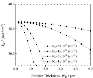
The short-circuit current density (Jsc) as function of emitter thickness and surface doping level is shown in Fig. 3. In this figure, it can be seen that the maximums of short-circuit current density curves are approximately 38.4 (mA/cm2) to all doping levels. However, the Jsc of higher doping level emitter solar cells are more sensitive than lower doping level emitter ones when the emitter thickness increases. This occurs because the emitter collection effi-ciency (ηE) decreases significantly due to band-gap nar-rowing and Auger recombination effects, as it is shown in Fig. 2. As it can be seen, low doping emitters are the best choice to form this region since they provide both high current density and a wide range of optimum thickness.
The internal quantum efficiency of a complete solar cell was calculated as the ratio between the total collected current density and the total photo-generated current den-sity for each wavelength. A complete analysis of the inter-nal quantum efficiency for each surface doping level and the correspondent optimized thickness has been made for
wavelengths (λ = 350-1100 nm) and it has been verified that there is no significant difference among them since the emitters have Gaussian profile.
In Fig. 4 the internal quantum efficiency as function of the wavelength (λ) is shown only for an optimized emitter with surface doping level Ns = 1x10¹⁹ (cm-3) and emitter thickness WE = 1.2 (µm). The base and BSF regions were previously considered.
According to Fig. 4 the homogeneous emitter presents a high internal quantum efficiency for the emitter wave-length range of interest λ = (350-600) nm; for instance, for λ = 400 nm the internal quantum efficiency is Qi(λ) ≅ 0.98. Figures 5 and 6 show open circuit voltage (Voc) and efficiency (η) as functions of emitter thickness respec-tively, considering different emitter doping levels. It can be seen that the limiting factor to achieve high efficiencies is open circuit voltage, which is determined by the saturation current density.
Figure 2. Emitter collection efficiency (ηE) vs. emitter thickness, admit-ting different doping levels (Ns) and two kinds of surfaces (passivated and non-passivated).
Figure 4. Solar cell internal quantum efficiency as function of wave-length. The emitter is admitted to be passivated with a surface doping level Ns = 1x10¹⁹ (cm-3) and WE = 1.2 (µm).
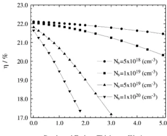
Figure 6 shows that homogeneous emitter solar cells have their best efficiencies (η ≅ 21.60-21.74%) when their doping levels are Ns = (1x10¹⁹ - 5x10¹⁸) cm-3 and their thicknesses are (1.2-2.0) µm. To simplify the calculations, the series resistance, rs has been considered as a constant, calculated to the following optimized emitter region case: surface doping level 1x1019 cm-3 and ≅ 1 µm emitter thickness (sheet resistance ≅ 100 Ω/ ). Therefore, the moderately doped and thick passivated emitters, besides requiring a simple fabrication technology, have high qual-ity. Thus, being of interest for industrial application.
3.3. Non-homogeneous emitters
Like it was made in the former case, the output parame-ters for complete solar cell were analysed. Non-homogene-ous emitters are made up of two regions: a passivated one (moderately doped) and a metal-contacted one (highly
doped). By examining Fig. 1, it can be seen that to reach low saturation current density (JoE) under metal-contacted surface emitters, this region must be highly doped. In this case, the thicker the emitter is, the lower JoE is. So in order to optimize non-homogeneous emitters, the surface doping level of Ns = 1x1020 cm-3 and 2 µm thickness (due to technological constrictions) were chosen. Short-circuit current densities (Jsc) are the same as homogeneous emitter solar cell ones, since it was considered the same metal grid shadowing factor Fm (3%) for both kinds of emitters. Open-circuit voltage (Voc) behavior of non-homogeneous emitter solar cells is quite different of homogeneous emitter solar cells - compare Figs. 5 and 7. Non-homogeneous emitters have their maximum Voc higher than the homogeneous ones.
Their maximum efficiencies are (η≅ 21.82-21.92%) with Ns = 1x10¹⁹ - 5x10¹⁸ (cm-3) and (1.2-2.0) (µm)
thick-Figure 6. Solar cell efficiency (η) as a function of emitter thickness (WE), considering different surface doping levels (Ns). The arrows indicate the emitter sheet resistance.
Figure 5. Solar cell open-circuit voltage (Voc) vs. emitter thickness (WE) with different doping levels (metal grid shadowing factor Fm = 3%).
Figure 7. Solar cell open-circuit voltage as a function of passivated emitter thickness (WE), considering different doping levels (metal grid shadowing factor Fm = 3%).
ness for passivated surface, as it can be seen in Fig. 8. Since the approximation of a constant (rs) has been made, effi-ciencies related to emitter sheet resistances higher than 100 Ω/ are overestimated.
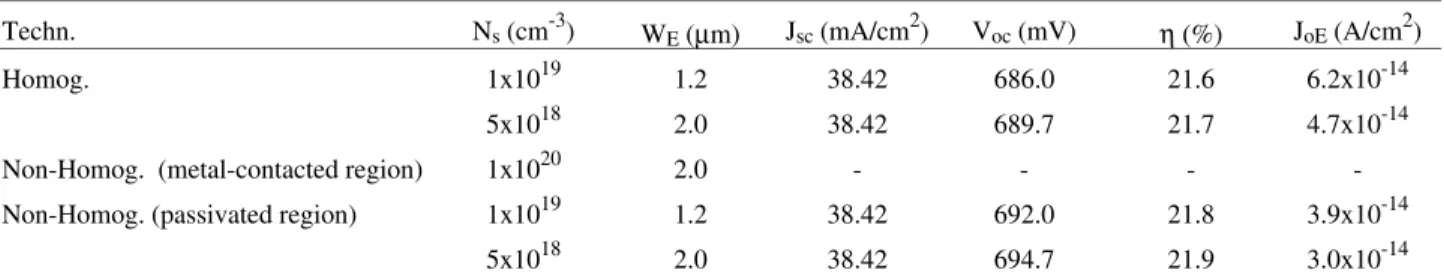
Table 2 shows a comparison between the optimum electrical output parameters for homogeneous and non-ho-mogeneous emitter solar cells, and the total emitter recom-bination as well.
It can be seen that the efficiencies in general are better for non-homogeneous emitter solar cells, the maximum efficiencies related to each different doping level are slightly higher, about 0.20 (%), than homogeneous ones.
As it has been commented previously, the open-circuit voltage is the limiting factor to reach higher efficiencies. When the kind of emitter is changed from homogeneous into non-homogeneous the emitter recombination current density decreases from 6.2x10⁻¹⁴ (A/cm2) to 3.9x10⁻¹⁴ (A/cm2), resulting in increase of approximately 1% in the open-circuit voltage for a passivated region with Ns = 1x10¹⁹ (cm-3) and WE = 1.2 (µm). Therefore, the non-homogeneous emitter solar cells are still responsible for the record efficiency laboratory solar cells, having more flexi-bility to obtain good ohmiccontacts. However, the com-plexity of the involved technology points the attention to the studies of Gaussian profile homogeneous emitter ones and their applications.
4. Conclusions
In this work a theoretical optimization of highly doped n-type region with Gaussian profile and complete solar cells have been made as functions of surface recombination velocity, emitter thickness and surface doping level. Fur-thermore, updated internal parameters have been used to take into account recent published changes. Considering these new conditions, homogeneous and non-homogene-ous were studied. Homogenenon-homogene-ous emitter solar cells show the maximum range of solar cell efficiency, η = 21.60-21.74% for Ns = 1x10¹⁹ - 5x1018 cm-3 with 1.2-2.0 µm emitter thickness range, corresponding to emitter sheet resistances 90-100 Ω/ respectively. Non-homogeneous emitter solar cells provide their best efficiencies η = (21.82-21.92%) with surface doping levels Ns = 1x1020 cm-3 with 2.0 µm thickness under metal-contacted surface and
Ns = 1x10¹⁹ - 5x1018 cm-3 with (1.2-2.0) µm thickness respectively under passivated surface. The non-homogene-ous emitter efficiencies are slightly better (0.20%) than homogeneous one, this relatively small difference is due to the fact that recombination in the base region also contrib-utes to limit the cell voltage. Despite non-homogeneous emitters are more complex, they are still relevant for ultra high efficiency solar cells. However, in practical silicon solar cells, the difference between the two kinds of emitters vanishes almost completely; since the contribution from the base region is still larger than that assumed in this paper, non-homogeneous provide more flexibility to obtain good ohmic contacts. The use of optimized homogeneous emit-ters with screen-printing metallization still awaits innova-tive ideas and experimental demonstration.
Acknowledgments
This work was supported by FAPESP under contract no 95/09435-0 and by Rhae/CNPq under contract n° 610157/94.
References
1. Cuevas, A.; Balbuena, M.A.; Galloni, R. Conf. Rec. 19th IEEE Photovoltaic Specialists Conference, New Orleans, p. 918-924, May 1987.
2. Cuevas, A.; Balbuena, M. 20th IEEE Photovoltaic Specialists Conference, v. 1, p. 429-434, 1988.
3. Aberle, A.; Warta, W.; Knobloch, J.; Vob, B. 21st IEEE Photo-voltaic Specialists Conference, v. 1, p. 233-238, 1990. 4. Cuevas, A.; Basore, P.A.; Girouit-Matlakoski, G.; Dubois, C. J.
Appl. Phys., v. 80, n. 6, p. 3370-3375, 1996.
5. Park, J.; Neugroschel, A.; Lindholm, F.A. IEEE Transactions on Electron Devices, v. ED-33, n. 2, p. 240-248, 1986. 6. Bisschop, F.J.; Verholf, L.A.; Sinke, W.C. IEEE Transactions
on Electron Devices, v. 37, n. 2, p. 358-363, 1991.
7. Lolgen, P.; Leguijt, C.; Eikelboom, J.A.; Steman, R.A.; Sinke, W.C.; Verhoef, L.A.; Alkemade, P.F.A.; Algra, E. 23rd IEEE Photovoltaic Specialists Conference, p. 236-242, 1993. 8. Green, M.A. Solar Cells: Operating Principles, Technology and
System Applications, Englewood Cliffs: Prentice-Hall, p. 78, 1982.
9. Sánchez, E.; Araújo, G.L. Solar Cells, v. 20, p. 1-11, 1987. 10. Cuevas, A.; Merchán, R.; Ramos, J.C. IEEE Transactions on
Electron Devices, v. 40, n. 6, p. 1181-1183, 1993.
FAPESP helped in meeting the publication costs of this article
Table 2. Comparison between the optimum output electrical parameters for homogeneous and non-homogeneous emitter solar cells.
Techn. Ns (cm-3) WE (µm) Jsc (mA/cm2) Voc (mV) η (%) JoE (A/cm2)
Homog. 1x10¹⁹ 1.2 38.42 686.0 21.6 6.2x10⁻¹⁴
5x10¹⁸ 2.0 38.42 689.7 21.7 4.7x10⁻¹⁴
Non-Homog. (metal-contacted region) 1x10²⁰ 2.0 - - -
-Non-Homog. (passivated region) 1x10¹⁹ 1.2 38.42 692.0 21.8 3.9x10⁻¹⁴