Flávia Cristina Monteiro Rocha
Licenciada em Ciências de Engenharia Física
Electrical characterization and modification
of low dimensional oxide semiconductors
for sensor applications
Dissertação para obtenção do Grau de Mestre em Engenharia Física
Orientadores: Prof. Doctor Ana Gomes Silva, FCT-UNL
Doctor Katharina Lorenz, IPFN, IST-UL
Júri:
Presidente: Prof. Doctor Isabel Catarino, FCT-UNL
Arguentes: Prof. Doctor João Cruz, FCT-UNL
“Electrical characterization and modification of low dimensional oxide semiconduc-tors for sensor applications”
Copyright © Flávia Cristina Monteiro Rocha, Faculdade de Ciências e Tecnologia, Universidade Nova de Lisboa.
Acknowledgments
The realization of this Theses allowed me to fulfill two childhood dreams this year: end-ing my Master in Physics Engineerend-ing and work at CTN.
For this, and for all the path until now, I would like to thank all of those who helped me to get here.
To Dr. Katharina Lorenz, who allowed me to be part of her incredible research team in CTN and be part of a true research project in physics. Thank you for allowing me to have all the time and freedom to experiment and ease my constant thirst of knowledge. But most of all, thank you for all of the good personal lessons: passion and dedication, along with a kindness, compassion and undying faith in all of those around her, making us want to do nothing but the best to make her proud. Thank you for your patience and understanding in the final step of the thesis.
To Prof. Dr. Ana G. Silva, my most heartfelt and big thank you. Not only for all the long and late hours of discussions, of teaching me, of sharing the most unbelievable amount of knowledge about everything and anything, but most of all, for the kindness that helped me in the most difficult of times, for listening and truly caring, without ever questioning. Thank you, from the bottom of my heart, for all the good professional, but much more important, personal orientation.
To Dr. Bianchi Méndez, Dr. Emilio Nogales, Dr. Maria Vila Santos and Dr.Carlos Viejo from Dpto. Física de Materiales, da Universidad Complutense de Madrid, Spain and Encarna Villora and Kiyoshi Shimamura from the National Institute for Materials Science, Japan, for all the samples that allowed this work to be done and also for the great amount of them, since I tend to finish all off the stock available.
ge-niality and making those incredible long beam days the best ones, even if you seem to disturb all the electronics around you. To Luis Ferreira, Carlos Cruz, Filomena, Jorge and Dª Vitória for making me feel home since day one. Also for all the good principles and showing that is possible to be a great professional and be a great college at the same time. I don’t think that CTN could survive without you.
To all my colleges. It’s amazing how many great people I have had the pleasure to
meet along these years. I wish you all the best and thank you for making everything more fun.
I want to give a really special and warm thank you to Marta e Francisco. I can say now that I will leave college richer for I have had the pleasure of working with you and
most important, be your friend. I still can’t believe the long nights of support, fun and laugher that we shared. Yes, I think we share a brain. And I adore you.
To Andreia, Cristina and Cristiana. You are always in my heart. To Evaldo for al-ways showing what friendship is made off. You are the meaning behind the word. This would not be possible without Caderno Diário days. For all the good advice and long talks, the friendship, the fun and helping me whenever I needed it, I want to thank Raquel Coutinho, Susana Sério and Dina Capelo. With you I had the most fun days.
To Dª Zé and Sr. Carlos, for always taking so good care of me, for all the great hours that we shared, the card games and for your kindness.
To my Mom, for she is the reason why I always believed I could follow my dreams. This was your great lesson to me, you made me believe that all dreams are pos-sible, that I could do anything. You never believe that the world is too small. Thank you for all the strength and fight. Thank you mom from my heart.
To the most important person in my life. To my half, my soulmate, my love, André Varelas. I genuinely don’t think that I would have made it without you. You are the rea-son behind all of this. You believe in me before all, you gave me strength, you were al-ways there. With you, life became the dream. I’m the most fortunate person in the world because I have you. It was the most fulfilling experience to achieve my dream side by side with you. Thank you for your Love.
Abstract
This work reviews the recent research on ion and UV irradiation of β-𝐺𝑎2𝑂3and α
-𝑀𝑜𝑂3 crystal structures. These crystalline materials belong to the transparent conductive oxides (TCOs) family due to their wide energy band gap and their transparency for visi-ble light. In-situ Electrical Characterization (EC) during proton and UV irradiation of the samples was carried out. Conductivity changes observed under ion and UV irradiation, designated respectively by Ion-Conductivity (IC) and Photoconductivity (PC), were measured and compared. Persistent conductivity phenomena were observed and ana-lyzed. For the electrical characterization, a recently acquired Parametric Analyzer was used and tested for the first time. A new home-built chamber for the EC, combined with other techniques such as Rutherford Backscattering Spectrometry (RBS), Particle-Induced X-Ray Emission (PIXE) and Ion-Luminescence (IL) was tested. Different crystal thicknesses were produced by crystal exfoliation using the scotch-tape technique, which was proved in this work, to be an inexpensive and efficient technique to obtained sam-ples with surfaces free of contamination. In order to perform the in-situ experiments, electrical contacts were produced and tested.
Resumo
Este trabalho vem na continuidade de trabalhos recentes sobre irradiação iónica e de UV em estruturas cristalinas de β-𝐺𝑎2𝑂3 e α-𝑀𝑜𝑂3.
Estes materiais cristalinos pertencem à família dos óxidos condutores transparentes (TCOs) devido ao seu largo hiato de energia e transparência à radiação no visível. Foi realizada Caracterização Elétrica (EC), in-situ, durante irradiação iónica e com UV. As alterações observadas para a fotocondutivade (PC), devido à irradiação UV, e para a iono-condutividade (IC), devido à irradiação com iões, foram analisadas e comparadas. Como resultado de ambos os tipos de irradiação, foi observado e analisado o fenómeno de condutividade persistente. Para a caraterização elétrica, foi usado e testado pela primeira vez, um analisador paramétrico recentemente adquirido pelo grupo. Foi testado um novo sistema experimental, projetado e construído no próprio laboratório para a caracterização elétrica in-situ em simultâneo com outras técnicas de caracterização que são Espetrometria de Retrodispersão de Rutherford (RBS), Emissão de Raios-X Induzida por Partículas (PIXE) e Iono-Luminescência (IL). Cristais de diferentes espessuras foram produzidos através de exfoliação mecânica utilizando a técnica da fita-cola, que provou ser eficiente e económico para a obtenção de amostras finas e livres de contaminação. Foram realizados contactos elétricos para a caracterização in-situ.
Contents
CONTENTS ... XI
LIST OF FIGURES ... XIII
LIST OF TABLES ... XVII
LIST OF ABBREVIATIONS ... XIX
INTRODUCTION ... 1
1.1 MOTIVATION ... 1
1.2 MAIN GOALS ... 2
STATE OF THE ART ... 3
OXIDE SEMICONDUCTORS STUDIED ... 5
3.1 GALLIUM OXIDE ... 5
3.2 MOLYBDENUM TRIOXIDE ... 8
TECHNIQUES AND EXPERIMENTAL SETUP ... 11
4.1 ELECTRICAL CHARACTERIZATION.PARAMETRIC ANALYZER. ... 11
4.2 MICROBEAM AND THE NEW SETUP ... 12
4.3 RUTHERFORD BACKSCATTERING SPECTROMETRY (RBS) ... 13
4.4 PARTICLE INDUCED X-RAY EMISSION (PIXE) ... 13
4.5 ANNEALING PROCESS... 14
4.6 UVLAMP ... 14
ELECTRICAL CHARACTERIZATION ... 17
5.1 SEMICONDUCTOR-METAL JUNCTIONS ... 18
5.2 SCHOTTKY DIODES CURRENT-VOLTAGE CHARACTERISTIC ... 19
5.3 CONTACTS PRODUCED AND RESULTS ... 20
6.1 ELECTROMAGNETIC RADIATION-MATTER INTERACTION ... 29
6.2 ION-SOLID INTERACTION ... 30
6.3 THE STOPPING POWER ... 31
6.4 SIMULATION OF PROTON IRRADIATION PROFILES ... 32
ION LUMINESCENCE ... 39
RADIATION INDUCED CONDUCTIVITY (RIC) ... 43
8.1 PERSISTENT PHOTOCONDUCTIVITY (PPC) ... 44
8.2 PERSISTENT ION-CONDUCTIVITY (PIC) ... 46
8.3 PERSISTENT INDUCED CONDUCTIVITY –EXPERIMENTAL RESULTS ... 47
8.3.1 Ga2O3 2D UV ... 48
8.3.2 Ga2O3 2D Proton Irradiation ... 50
8.3.3 Ga2O3 1D UV ... 51
8.3.4 Ga2O3 1D Proton Irradiation ... 53
8.3.5 MoO3 2D Flake UV ... 54
8.3.6 MoO3 2D Flake Proton Irradiation... 55
8.3.7 MoO3 2D nanoplate UV ... 56
8.3.8 MoO3 2D nanoplate Proton Irradiation ... 58
8.4 PHOTO INDUCED (UV) PERSISTENT CONDUCTIVITY.DISCUSSION. ... 60
8.4.1 Ga2O3 2D ... 60
8.4.2 Ga2O3 1D UV ... 65
8.4.3 MoO3 2D Flake UV ... 66
8.4.4 MoO3 2D Nanoplate UV ... 67
8.5 PROTON-ION INDUCED PERSISTENT CONDUCTIVITY.DISCUSSION ... 68
8.5.1 Ga2O3 2D proton ... 69
8.5.2 Ga2O3 1D ... 70
8.5.3 MoO3 2D flake ... 72
8.5.4 MoO3 2D nanoplate ... 73
8.5.5 Devices ON/OFF current Ratios to UV and Proton Irradiation. Thickness relation 73 CONCLUSIONS AND FUTURE WORK ... 75
List of figures
Figure 3.1 Crystal Structure of Gallium Oxide [15] ... 6 Figure 3.2 Left: picture of beta Gallium oxide [16] Right: Scanning Tunneling Microscopy (STM) image of Gallium oxide (100) surface [12]. ... 6 Figure 3.3 - Left side: SEM (Scanning Electron Microscope) images of the nanostructures grown when doped in presence of 𝑆𝑛𝑂2. Right side: SEM image of a branch of the doped nanowire [18] ... 7 Figure 3.4 - Left side: Nanowire tested in this work, with silver contacts and microprobes of the parametric analyzer. Right side: an amplified image of the nanostructure. ... 7 Figure 3.5 - Crystal structure of molybdenum trioxide [20]... 8 Figure 3.6 (a) Photograph of laminar crystals (b) and (c) SEM images of the flakes evidencing the laminar structure of the grown crystals [21]. ... 9 Figure 3.7 - SEM images of MoO3 nanoplates with rectangular shapes and hexagonal shapes and respective crystal axes [21]. ... 9 Figure 4.1 Left: Scheme of the combined techniques and overview of the new setup. Middle: the new chamber lid; Right: amplified views of the printed circuit board (PCB) for the electrical measurements. ... 12 Figure 4.2 RBS schematic of the physical principle behind backscattered particle and the relation between the energy and depth of the material.[22] ... 13 Figure 4.3 PIXE schematic of the physical principle behind X-ray emission from the sample[22]. ... 14 Figure 5.1 Scheme of a typical band structure for a semiconductor. ... 17 Figure 5.2 One dimensional energy diagram for the interface region of a metal semiconductor junction after contact ... 19 Figure 5.3 – Top view scheme of a metal semiconductor metal (MSM) configuration used to make the devices in this study. It has a layer made of an insulator material that was the substrate for the crystal (semiconductor) and two metal contacts deposited on top. ... 20 Figure 5.4 Scheme of the device built for testing gallium oxide and molybdenum trioxide crystals with kapton as a substrate and with tips ... 21 Figure 5.5 - Ga2O3 and MoO3 with indium contacts annealed in Rapid Thermal Annealing (RTA), at 1x10⁻⁵
Figure 5.11 - Schematic of the three contact configurations performed with silver (represented in grey) and Ga2O3 (represented in black) and respective I-V curves for a) bulk conductivity along the a crystal axis b)
conductivity in the c direction crystal axis and c) conductivity in the direction b crystal axis. ...27
Figure 6.1 - Typical Bragg Curve represented as a function of the distance accomplished for a light energetic particle in a heavy matrix. ...31
Figure 6.2 - Comparison between nuclear (red data and red scale) and electronic stopping power (blue data and blue scale) for protons in gallium oxide. ...32
Figure 6.3 - SRIM simulation plots for stopping power for hydrogen ion irradiation for a gallium target (top left plot) [47] and for molybdenum target (top right plot) [48]. ...33
Figure 6.4 - Comparing SRIM simulation assuming a bulk geometry (left) and using the program Ion Range And Damage In Nanostructures (Iradina) [34] assuming the correct geometry of a nanowire. ...34
Figure 6.5 - TRIM simulation showing the ion tracks with depth and in transverse view for a 2 MeV proton beam in Ga2O3 ...35
Figure 6.6 -Total displacements of both gallium and oxygen caused by the passage of the beam; Ionization profile in gallium oxide by the electronic collisions with the ion beam, distribution of protons in gallium oxide. ...35
Figure 6.7 - TRIM simulation showing the ion tracks with depth and in transverse view for a 2 MeV proton beam in MoO ...36
Figure 6.8 - Ionization profile of molybdenum oxide caused by the passage of the 2MeV proton beam in molybdenum oxide; Total Displacements of both molybdenum and oxygen, Proton distribution in molybdenum oxide. ...36
Figure 6.9 - Ionization profile of the nanowire where the beam enters the nanowire perpendicular to the x-axis. ...37
Figure 6.10 - Displacements of gallium and oxygen along the x-y plane of a 900 nm diameter Ga2O3 nanowires irradiated with 2 MeV protons. ...37
Figure 7.1 - Relative position of the incident ion beam to the crystal. ...39
Figure 7.2 – 𝛽 − 𝐺𝑎2𝑂3 luminescence mechanisms schematic (from [35]). ...40
Figure 7.3 - PIXE and RBS spectra for a gallium oxide sample irradiated with 2 MeV protons ...40
Figure 7.4 - Ion Luminescence spectrum from the 𝐺𝑎2𝑂3 material when being irradiated (horizontal scanning) with protons. ...41
Figure 7.5 – a) Picture of the gallium oxide flake b) blue emission during proton irradiation (lateral beam scanning) c) blue emission observed during irradiation with UV light. ...41
Figure 7.6 – Final 250 seconds of the luminescence spectrum of the gallium oxide during proton irradiation. ...42
Figure 8.2 – Normalized currents for the four cycles ON/OFF represented in the inset picture (a) and respective fitting curves using the PPC model for the rise (red) and for the decay (blue) cycles using equations 8.9 and 8.10 respectively. ...48
Figure 8.3 I-V curves for -Ga2O3 #1 flake before, during and after irradiation with UV light ...49
Figure 8.4 – Normalized I(V)-t curves for -Ga2O3 #2 flake irradiated with a 2 MeV proton beam (a) inset picture correspondent to the in-situ measured current ...50
Figure 8.5 –I-V curves for -Ga2O3 #2 flake irradiated with a 2 MeV proton beam. ...51
Figure 8.6 –I-V curves for the Sn--Ga2O3 nanowire irradiated with visible light. ...52
Figure 8.7 –I(V)-t curves for the Sn--Ga2O3 nanowire. Decay and rise times for the three cycles ON/OFF represented in the inset picture (a) and respective fitting curves using the PPC model for the rise (red) and for the decay (blue) cycles. ...53
Figure 8.8 - I(V)-t curves for Sn--Ga2O3 nanowire irradiated with 2 MeV proton beam ...54
Figure 8.9 – PIXE images of MoO3 flake (Table 5.1, Chapter 5) of the L 1 and K 1 X-ray lines of Molybdenum ...55
Figure 8.11 – Normalized currents for the two cycles of UV ON/OFF represented in the inset picture (a) and respective fitting curves using the PPC model for the rise (red) and for the decay (blue) cycles ... 57 Figure 8.12 – MoO3 nanoplate UV study after proton irradiation... 58
Figure 8.13 - PIXE map of MoO3 nanoplate (Table 5.1, Chapter 5) of the L 1 X-ray line of Indium ... 58
Figure 8.14 - I(V)-t curves for MoO3 nanoplate irradiated with 2 MeV proton beam (a) inset picture
correspondent to the in-situ measured current ... 59 Figure 8.15 – I(V) –t test of the influence of the luminescence of sapphire on the molybdenum trioxide sample ... 60 Figure 8.16 Scheme of the electric circuit studied and the correspondent one-dimensional junction scheme without any UV light present... 61 Figure 8.17 - Scheme representing the input function, Iconstant(t), the S (representing the response of the device) and I(t), the output function ... 62 Figure 8.18 –I(V)-t plot for one normalized rise(black) and one decay(grey) curve for the 2D Ga2O3UV in
order to determine respectively both τOn and τOff when the current is 63.2% or 38.2% of the initial value. ... 63
List of tables
Table 1 – Thickness of the MoO3 samples studied ... 10
Table 2 - High Power UV-Vis Fiber Light Source lamps - L120290 [26] ... 14
Table 3 - First Order Response output function ... 63
Table 4 - Time constants for rise and decay of the plot in Fig. 8.2 ... 64
Table 5 - Values of from the fit with PPC model, for each cycle ... 64
Table 6 - Time constants for rise and decay of the plot in Fig. 8.7 ... 66
Table 7 -Values of γ from the fit with PPC model, for each cycle in Fig. 8.7 ... 66
Table 8 and Table 9 – Values of τ from the fit with PPC model, for each cycle in Fig. 8.11 and 8.12 respectively. ... 67
Table 10- UV test for MoO3 nanoplate before proton irradiation ... 68
Table 11- UV test for MoO3 nanoplate after proton irradiation ... 68
Table 12 – Proton Induced Conductivity constant time for 2D gallium oxide flake correspondent to Fig. 8.4 ... 69
Table 13 – Proton Induced Conductivity parameters for 2D gallium oxide flake of Fig. 8.4 ... 69
Table 14 – Proton Induced Conductivity time constant for 1D gallium oxide nanowire correspondent to Fig. 8.8 ... 71
Table 15 – Proton Induced Conductivity parameters for 1D gallium oxide nanowire correspondent to Fig. 8.8 ... 71
Table 16 – Proton Induced Conductivity time constants for a 2D molybdenum trioxide flake correspondent to Fig. 8.10 ... 72
Table 17 – Proton Induced Conductivity parameters for 2D molybdenum trioxide flake correspondent to Fig. 8.10 ... 72
Table 18 – Values of τ from the fit with PPC model, for Fig. 8.14 ... 73
Table 19– proton irradiation for MoO3 for Fig. 8.14 ... 73
List of abbreviations
UV Ultraviolet
Ga2O3 Gallium Oxide
MoO3 Molybdenum Trioxide
TCOs Transparent Conductive Oxides EC Electrical Characterization
IC Iono-Conductivity
PC Photoconductivity
RBS Rutherford Backscattering Spectrometry PIXE Particle-Induced X-Ray Emission
Il Ion-Luminescence
Si Silicon
GaAs Gallium Arsenide GaN Gallium Nitride
2D Two Dimensional
MSM Metal-Semiconductor-Metal
Ga Gallium
O Oxygen
STM Scanning Tunneling Microscope
SnO2 Tin Dioxide
HRTEM High Resolution Transmission Electron Microscopy
VS Vapor-Solid
Mo Molybdenum
Introduction
1.1 Motivation
Semiconductors exhibit a wide spectrum of phenomena, in terms of electrical con-ductivity or in terms of optical effects. They have been studied since 1920’s and in 1940 the first transistor was invented by Shockley, Bardeen and Brattain [1]. Since then, tech-nology has undergone a great development and our daily life is nowadays unthinkable without microelectronics present in televisions, mobile phones, personal computers etc. In addition to conventional semiconductors such as Si and GaAs, in the last decades the interest in more complex semiconductor families such as nitrides (e.g. GaN) and metal-oxides has been rising [2]. Furthermore, nanostructures such as nanowires or ultrathin systems are expected to contribute to the miniaturization of electronics devices as well as to the development of novel applications.
One of the interesting characteristics of low dimensional crystal structures is relat-ed with their dimensional limit leading to different atomic confinement conditions in space. Furthermore, their large aspect ratios lead to high surface area to volume ratios increasing effects related to the semiconductor surface. In the case of 2D materials, dif-ferent types of forces act between atoms of adjacent planes and between atoms belonging to the same plane, the latter being much stronger than the former allowing the easy pro-duction of ultrathin systems.
1.2 Main Goals
The main purpose of this work was to study the electrical properties, such as pho-toconductivity and ion-conductivity, of low dimensional semiconductor oxides and evaluate their response as radiation sensors under UV and proton irradiation.
The first task to be carried out in this thesis was the production and optimization of the electrical junctions for the materials in study, i.e. gallium oxide and molybdenum oxide. In fact, this was a challenging task. Due to the bandgap characteristics of these ox-ides (wide bandgap) and their irregular shape at nanoscale, junctions of different shape and arrangement need to be implemented. In fact, current-voltage curves of devices built with the same metallic contacts and produced under the same conditions can present different behaviors, showing ohmic to Schottky characteristics. These different results are attributed to interfacial chemistry and natural surface disorder [3]. Electrical junction properties need to be thoroughly understood in order to allow the currents (often in the nano-Ampère range) to be measured with low noise and avoiding misinterpretation of physical phenomena that can occur during the measurements [4].
State of the art
Semiconductor nanostructures are interesting materials for many applications such as electromagnetic radiation sensors, particle interaction sensors, gas sensors, nano-electronics and nano-light emitters in nanoscale dimension devices [6]. Because of their electronic structure, with well-defined band gap, defect centers that appear in the crystal structure will cause energy levels to appear in the forbidden band gap. These energy levels or traps, may significantly influence the conductivity of the electric device, since they influence the recombination mechanisms of free electrons and holes. Evaluating the electronic behavior of the device at the same time that irradiation processes are taking place will allow the study of the effects caused by ionization and defect formation pro-cesses induced by the irradiation. These studies can also be a good basis for further stud-ies on ion implantation [7].
Semiconductor oxides have a large band gap and such characteristic provides a good base for optical transparency for electronic devices. This characteristic could induce to think that these materials are inapt for electronic conduction. However, they are proved to be good conductors and since they continue to be transparent to visible light this new class of materials is designated by Transparent Conductive Oxide semiconduc-tors (TCOs), as reported by Hosono [8].
Also, some semiconductor oxides, such as thin crystalline films of MoO3 and
Ga2O3, are considered to be in a sense 2D materials due to the nature of the forces
estab-lished between adjacent crystal planes which are of Van der Waals type.
According to Feynman[9], Van der Waals’ forces arise from the fact that the elec-tron charge distribution is not isotropic around the nuclei, when in a molecular struc-ture, being higher between two adjacent nuclei. This anisotropic charge distribution cre-ates a dipolar moment proportional to (1\R7) where R is the distance between the
oms. An attractive force arises between such anisotropic molecules due to the Coulomb forces between the negative electron cloud of one molecule and the positive side of an-other molecule. The same considerations are made about covalent bonds but for distanc-es R in the order of the atomic radii, which reflects a dipolar moment proportional to 1/R, leading to much stronger forces than for the Van der Waals case.
Due to the forces established between adjacent crystalline planes being Van der Waals in opposition to the covalent bonds made between atoms from the same plane, these materials are easily exfoliated, like in graphene, the most famous case of such ma-terials since 2010 when the Physics Nobel Prize was awarded for the development of a one monolayer graphene device produced by mechanical exfoliation using scotch tape [10].
In order to functionalize the semiconductors, Metal-Semiconductor-Metal (MSM) devices were made. MSM photodetectors have been studied and shown to be faster than photodiodes. It has been reported that they also have a wider wavelength sensitivity, some reaching hundreds of gigahertz [11].
Oxide Semiconductors Studied
The crystals studied in the present work were produced by other groups. Exfoliat-ed samples were obtainExfoliat-ed by our group.
There are many studies made about metal oxide thins films, but not as much as about single crystals oxides, where the most existing studies are about zinc oxide and titanium oxide [12].
3.1 Gallium oxide
The material is both conducting and transparent and this is an extremely important feature for future electronic devices [13].
β-𝐺𝑎2𝑂3 has the largest band gap (between 4.8 and 4.9 eV), that corresponds to 253-258 nm, of all Transparent Conductive Oxide (TCO), which means that it is transpar-ent in the visible and UV wavelength region [14].
The beta phase is the most stable form of gallium oxide, with a monoclinic base centered crystal structure (see Fig. 3.1), where Ga has different coordination numbers with tetrahedral and octahedral symmetry, while O resides at the corners of these tetra-hedral and octatetra-hedral.
Figure 3.1 - Crystal Structure of Gallium Oxide [15]
The gallium flakes studied were taken and then exfoliated from the gallium bulk single crystals samples (Fig. 3.2), grown using the floating zone technique in Japan, with 99.99% purity gallium oxide powders, by a set-up equipped with four halogen lamps and the corresponding ellipsoidal mirrors and were cleaved on the (100) plane [16].
The float zone crystal growth, pioneered by Samsung AG, produces highly pure single crystals using melt of a material and growing single crystals oriented by a seed that is in the center of the melt. The melt is pushed along the seed by swirling the seed at a constant speed. It is a technique appropriate for growing crystals with diameters lower than 150 nm, because it needs surface tension to be strong enough to keep the liquid in place around the seed.
Because this procedure is done in vacuum or in an ambience of inert gases, the crystals produced have high purity [17].
Figure 3.2 - Left: picture of beta Gallium oxide [16] Right: Scanning Tunneling Microscopy (STM) image of Gallium oxide (100) surface [12].
The gallium oxide nanowires (Fig. 3.3) were grown and doped with tin by the group of
Departamento de Física de Materiales at Universidad Complutense De Madrid, Facultad De
Ciencias Físicas.
Figure 3.3 - Left side: SEM (Scanning Electron Microscope) images of the nanostructures grown when doped in presence of 𝑆𝑛𝑂2. Right side: SEM image of a branch of the doped nan-owire [18]
Figure 3.4 - Left side: Nanowire tested in this work, with silver contacts and microprobes of the parametric analyzer. Right side: an amplified image of the nanostructure.
The doped gallium oxide nanowire are grown by a two-step thermal oxidation process:
1) The nanowires are grown by the vapor-liquid-solid (VLS) method, where pellets were made of compressed 𝐺𝑎2𝑂3 powders of 99.999% purity and were used as a substrate for the metallic gallium precursor. This process was done in a tubular oven, for 10 h, at 1150 ºC with a flux of Argon of 0.8 l/minute.
2) The second step, were the doping was achieved, the samples produced were put in the oven first at 1100 ºC, for 1 hour, and then again for 1500 ºC, for 15h, both with a flux of Argon of 0.8 l/minute and in the presence of metallic gallium and 𝑆𝑛𝑂2 powder.
The nanowire studied in the present work has a silver contact has shown in Fig. 3.4 (left side) and has 800 micrometer length (same figure, right side) and 900 nanometer radius [18].
3.2 Molybdenum trioxide
Molybdenum trioxide crystals have a wide band gap between 2.9 and 3.2 eV. Both -MoO3 phase (see Fig. 3.5), confirmed by high
resolution transmission electron microscopy (HRTEM)[19].
Figure 3.5- Crystal structure of molybdenum trioxide [20].
Figure 3.6 - (a) Photograph of laminar crystals (b) and (c) SEM images of the flakes evidenc-ing the laminar structure of the grown crystals [21].
In SEM images (Fig. 3.6 c) the laminar structure of the flakes can be observed. This characteristic allowed exfoliated samples to be produced by mechanical exfoliation (us-ing the scotch tape technique).
The Molybdenum oxide nanoplates were grown by the same method as the flakes, the VS method, but the thermal treatment was done at 800 ºC, for 40 minutes with an Air flux of 1.2 l/min.
Figure 3.7 - SEM images of MoO3 nanoplates with rectangular shapes and hexagonal shapes and respective crystal axes [21].
The air flux favors the transportation of the material to a low temperature region inside the walls of the tubular furnace, where the material sets and starts to nucleate forming the nanoplates.[21]
The samples’ thickness studied in this work (Table 1), were determined by Ruther-ford Backscattering Spectrometry (RBS), where measuring the areal density of the layer and using the density of MoO3 from literature [21], allowed the calculation of the typical
width of the nanoplates and of the MoO3 flakes produced by mechanical exfoliation
Table 1 – Thickness of the MoO3 samples studied
Density of MoO3 4.69 𝑔
𝑐𝑚3
Areal Density determined by RBS
Nanoplate 200 cmμg2
Exfoliated Flake 2900 μg
cm2
Thickness Nanoplate 400 nm
Techniques and experimental setup
In this chapter, the main techniques used to characterize and to modify the sam-ples are summarized.
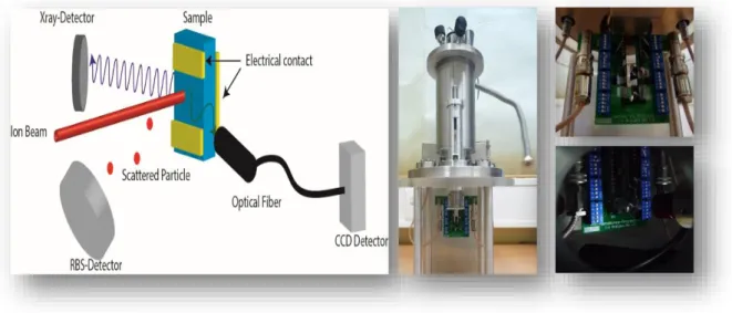
A new home-made chamber in the Van de Graff accelerator, conceived by LATR (CTN) team, is used for electrical in-situ measurements simultaneously with several oth-er techniques, namely RBS, PIXE and ion luminescence. Annealing processes woth-ere poth-er- per-formed in an ANNEALSYS AS-One Rapid Thermal Processing cold wall chamber fur-nace. The proton beam experiments were developed at the Plasma and Nuclear Fusion Institute (IPFN), situated at the Laboratory of Accelerators and Radiation Technologies (LATR) inside the Nuclear and Technological Campus (CTN) of Instituto Superior Téc-nico (IST).
4.1 Electrical characterization. Parametric Analyzer.
The current versus voltage (I-V) curves were measured using an Agilent B1500A parametric analyzer, used in general for semiconductor device characterization. The par-ametric analyzer measures the I-V curves, and I (t) curves, current as a function of time, for a constant applied voltage. It is equipped with 4 MPSMU (Medium power source/monitor unit) which allow voltages up to 100V to be used simultaneously. In or-der to do the correct measurements and with as little noise as possible, the correct con-nectors had to be installed. SMU can be connected to electric contacts, such as crocodile clips or the micro positioners, by tri-axial cables because an extra layer of insulation is a requirement when very low currents (such as nA and lower) are going to be measured.
The 20 micrometers movement resolution micro positioners from Everbeing pro-vide fine adjustments in all 3 dimensions and were associated with one micrometer tungsten tips (T20-10). This metal tip can provide the electric contact directly on top of
some samples. These tips are very useful in order to perform instant and safe contacts of very little structures preventing damage and without making permanent contacts. In or-der to make measurements as reproducible as possible and for example avoid effects of charge accumulation during the measurements, a rectangular voltage function is applied to the sample with the time of zero voltage much longer than the time of voltage applied; 20 ms voltage on and 180 ms voltage off.
4.2 Microbeam and the new Setup
The Van der Graff generator can produce a beam of 2.5 MeV protons or alpha par-ticles. The Van de Graff accelerator is equipped with three beam lines that allow the use of techniques such as RBS, PIXE and IL. The nuclear microprobe (Oxford Microbeams®) allows focusing the beam by means of quadrupole magnets reaching lateral resolution of 1.5 m. The lateral resolution enables the analysis of small and heterogeneous samples with more precision and as is the case of the structures used in this thesis. To these tech-niques was added the electrical characterization for measurements in-situ using the par-ametric analyzer (Fig. 4.1).
Figure 4.1 - Left: Scheme of the combined techniques and overview of the new setup. Mid-dle: the new chamber lid; Right: amplified views of the printed circuit board (PCB) for the electri-cal measurements.
4.3 Rutherford Backscattering Spectrometry (RBS)
Rutherford backscattering spectrometry (RBS) is a nuclear technique that is widely used for surface analysis of solids. Basically a target is bombarded with ions (typically alpha particles or protons of 0.5 to 4 MeV energy). The energy of the backscattered ions, coming from the surface and from the bulk, are measured in a solid state detector giving information on the elemental composition of the layers with a depth resolution of several nm at the surface. The energy of the backscattered particle, coming from the surface, is given by a simple relation between the energy before and after the collision, where the k factor, or kinematical factor, gives the ratio between the two.
Figure 4.2 - RBS schematic of the physical principle behind backscattered particle and the relation between the energy and depth of the material.[22]
The difference between the energy of the backscattered particles coming from the bulk, at a certain depth, and from the surface can be related in order to determine the sample thickness (see schematic in Fig. 4.2). The parameters involved and dependent on the material properties are the kinetic factor and the stopping power [23].
4.4 Particle Induced X-Ray Emission (PIXE)
PIXE is a nuclear technique that determines the elemental composition of a materi-al, by analyzing the X-Ray emission prevenient from the atomic interactions when the sample is exposed to an ion beam. Since X-rays are specific for each element the compo-sition of the samples can be determined. While RBS gives more depth information about a material, PIXE is useful to distinguish elements with similar mass and it is very sensi-tive to low concentrations of contaminants.
with a probability given by the cross section and if they suffer little attenuation, they will emerge from the surface (see schematic in Fig. 4.3).
Figure 4.3 - PIXE schematic of the physical principle behind X-ray emission from the sam-ple[22].
Both PIXE and RBS were used mainly to position the samples while being irradiat-ed and to give an estimation of the samples thickness.
4.5 Annealing Process
Rapid thermal annealing (RTA) processes can achieve temperatures over 1000 ºC, in few minutes or less, using high power lamps or lasers. In the present work, an AN-NEALSYS As-one furnace was used. This furnace can perform annealing from room temperature to 1500 ºC, with ramp rates up to 200ºC/s in different atmospheres (Ar, N, air) and in high vacuum (up to 10-6 mbar) [24]. Annealing processes are known for many
applications especially for semiconductor technologies once they can change interfaces, change steps of growth, repair damage caused by ion implantation [2] and relo-cate/activate dopants in films. So RTA can improve the quality of contacts by improv-ing the adhesion of the metal and reducimprov-ing the presence of defects [25].
4.6 UV Lamp
Using a High Power UV-Vis Fiber Light Source, L10290 model of Hamamatsu, with a deuterium and a tungsten/halogen lamp providing light with wavelengths be-tween 200 nm and 1600 nm, respectively UV radiation and infrared.
Table 2 - High Power UV-Vis Fiber Light Source lamps - L120290 [26]
Electrical Characterization
Gallium oxide and molybdenum oxide are intrinsic n-type semiconductors [27] [28]. A description of semiconductors will be given in the next section and the generality of crystalline semiconductors physics will be briefly described. Conductive mechanisms and junctions will be reviewed in order to understand the current-voltage characteristics of the devices.
In metals, and according to the band theory of solids, the valence and conduction bands overlap. The Fermi level is at the top of the occupied states in the conduction band. In semiconductors, on another hand, the valence and conduction bands are well separated by a bandgap (Eg) (Fig. 5.1). At zero kelvin, electrons are all in the valence
band, but at room temperature some electrons have enough energy to overcome this gap and fill available quantum states in the conduction band.
Figure 5.1 - Scheme of a typical band structure for a semiconductor.
Insulators have the same characteristics as semiconductors, but their band gap en-ergy is too high to be overcome by thermal excitation. However, there are no fixed rules on how to distinguish semiconductors from insulators. Many materials nowadays con-sidered wide band gap semiconductors, were once called insulators.
When electrons are excited to the conduction band (CB), holes are being created in the valance band (VB), leading to currents of negative charges (electrons) and currents of positive charges (holes) in opposite directions, i.e., they are bipolarized. In pure semi-conductors there is an equilibrium between electrons in the CB and holes in the VB. This equilibrium can be changed by doping the semiconductor with impurities giving rise to different conduction behaviors, dependent on the type of impurities: electron donors or electron acceptors, creating energy states within the bandgap closer to the conduction band (n-type semiconductor) or closer to the valence band (p-type semiconductor). 5.1 Semiconductor-Metal junctions
Metal-Semiconductor contacts were first comprehensively described by Schottky and for that reason Metal-Semiconductor devices are called Schottky barrier devices. This description is usually applied to devices where the current-voltage characteristics are clearly non-ohmic. One way to describe the semiconductor-metal junction at their interface is by aligning their Fermi energy level [1].
Two different contact behaviors can occur between a metal and a semiconductor; and as said before, it can form a Schottky contact with a rectifying behavior or it can form an ohmic contact.
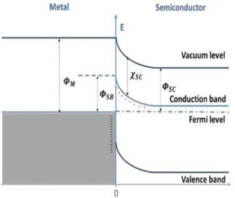
When an n-type semiconductor is brought in contact with a metal, the Fermi levels align and electrons flow from the semiconductor to the metal causing a band bending at the semiconductor-metal interface (Fig.5.2). The potential barrier build up in this way will eventually stop this electron flow and equilibrium is reached. Here, assumptions are being made that surface states are not playing a major role in the contacts established.
Electron diffusion takes place because of the different chemical potential of the last filled levels of both materials. Electrons can flow from the semiconductor to the metal without any given energy until they accumulate in the regions closer to the interface and an opposite electric field appears canceling the spontaneous flow, so an energy given by
Figure 5.2 - One dimensional energy diagram for the interface region of a metal semicon-ductor junction after contact
In Fig.5.2 𝛷𝑀, represents the work function of the metal,𝛷𝑆𝐶, is the work function of the semiconductor,𝜒𝑆𝐶, represents the electron affinity of the semiconductor and 𝛷𝑆𝐵, represents the energy of the Schottky barrier considering that only bulk effects are partic-ipating on the represented n-type semiconductor-metal junction. The Schottky barrier is highly dependent on the quality and purity of the interface area (a region of a few na-nometers between the semiconductor and the metal), as well as the number of surface state.
When equilibrium is achieved, the energy of the Schottky barrier, 𝜙𝑆𝐵 , is given by comparing the energy difference between the work function of the metal, 𝜙𝑀 , and the electron affinity of the semiconductor,𝜒𝑆𝐶
𝜙𝑆𝐵= 𝜙𝑀− 𝜒𝑆𝐶 (5.1)
Ohmic contacts are established between a highly doped semiconductor and a met-al, where the charge concentration reduces the band bending given by 𝜙𝑆𝐵.
5.2 Schottky diodes current-voltage characteristic
Figure 5.3 - Top view scheme of a metal semiconductor metal (MSM) configuration used to make the devices in this study. It has a layer made of an insulator material that was the substrate for the crystal (semiconductor) and two metal contacts deposited on top.
This configuration is called back-to-back Schottky devices [3]. The devices are usu-ally referred to as metal semiconductor metal (MSM) devices.
5.3 Contacts produced and results
For the in situ electrical characterization measurements of 𝐺𝑎2𝑂3 and 𝑀𝑜𝑂3 while being either irradiated with charged particles or excited with UV light, MSM devices were made. For the present case it did not matter if the contacts were rectifying or ohmic, because the main goal was to make stable contacts. As for the case of gallium oxide it was relatively easy to establish contacts, but many attempts were made in order to measure the conductivity of the molybdenum oxide flakes until some conclusive meas-urements could be done. Although gallium oxide has a wider band gap and one would think it would be more difficult to do the MSM junction, molybdenum oxide flakes are far more brittle than the gallium oxide crystals and therefore far more difficult to make a M-S junction. In the next paragraphs the procedures made in order to establish the con-tacts and the I-V characteristic curves of each device will be described. The first contacts were made in bulk samples due to the facility of making contacts in bigger samples and to understand the material behavior before the production of thinner samples.
Due to the brittleness of both crystals, hard insulator substrates, like glass, proved to be inadequate for measurements with the micro positioners because the tips would disrupt in pieces. Since these devices were going to be irradiated with high energy pro-tons, scotch tape was not a good solution as well.
The substrate chosen was Kapton Tapes, made from Kapton ® polyimide film with
Figure 5.4 - Scheme of the device built for testing gallium oxide and molybdenum trioxide crystals with kapton as a substrate and with tips
Many tests were carried out in order to check the absence of ion conductivity for this tape, since nonzero ion conductivity was reported in reference [29]. Fortunately, the irradiation did not lead to current flow in the tape, probably due to the fact that the sili-cone adhesive side was not conductive and not sensitive to proton irradiation.
From the available materials, those with closer work function to the band gap of gallium oxide (~4.9 eV)[5] and molybdenum oxide(~3.2 eV) [30] were chosen. The simi-larity between these potentials decreases the resistance of the Schottky contact and con-sequently decreases the necessary potential difference across the device necessary to get current flow. [31]
Aluminum, silver, tungsten, gold, indium and tin contacts were tested.
The indium used to make contacts is from GoodFellow and has a high purity. The aluminum used is traditional aluminum foil and the tin used is traditional soldering ma-terial.
To the semiconductors glued with the Kapton tape, bits of each of the metals avail-able were deposited on top, with the help of tweezers, has can be observed in Fig.5.3, allowing the electrical studies ahead to be performed.
Contacts and samples were then annealed in a tubular furnace, at 200 ºC, for six minutes, in air, for the tin, aluminum and indium metals in both crystals.
None of the metals made a good MS junction, which is probably due to an oxide insulator layer created during the annealing exposed to the oxygen in the atmosphere.
In order to address this, the same contacts were tested for both semiconductors us-ing a rapid thermal annealus-ing furnace in controlled ambient.
The MSM devices were annealed at 200 ºC, for 120 seconds in a vacuum of 1 ×
10−5mbar.
in the same conditions to the same samples but for higher temperatures and longer times.
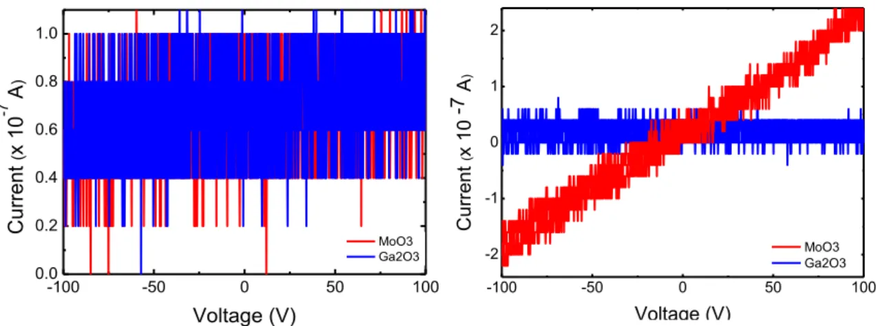
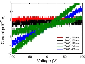
The I-V characteristic curves for the RTA results for the indium contacts can be ob-served in Fig. 5.5. For both semiconductors it’s represented the first annealing, at 180 ºC for 120 sec, and for the last annealing, performed at 200 ºC, 240 sec, both at 1x10⁻⁵ mbar.
As can be observed in the right plot of Fig.5.5, there is a lot of noise for both semiconduc-tors.
Figure 5.5 - Ga2O3 and MoO3 with indium contacts annealed in Rapid Thermal Annealing
(RTA), at 1x10⁻⁵ mbar Left: 180 ºC, 120 sec and Right: 200 ºC, 240 sec
Comparing the right and left plots, the gallium oxide sample did not reveal any improvement using this approximation.
However, for the case of the molybdenum oxide sample, a clear change can be ob-served.
In order to understand if this was a material response more annealing tests were performed in another sample made in the same conditions.
-100 -50 0 50 100
-2 -1 0 1 2 Curr ent ( x 10 -7 A ) Voltage (V) MoO3 Ga2O3
-100 -50 0 50 100
Figure 5.6 - Annealing tests performed in RTA for a second sample of molybdenum triox-ide, for increasing temperatures and exposition time.
The same results were observed for this second sample and are shown in Fig. 5.6. In this plot is also evidenced the electrical hysteresis typical of bath quality contacts. For example, the green curve belongs to one current-voltage measurement and shows two different branches were one belongs to positive current and another to negative current. If the contact was well made, the resistance of the sample would be the same since the measuring conditions are the same.
For both samples the conductivity is seen to increase with annealing temperature and, in contrast to Ga2O3, an ohmic behavior is observed.
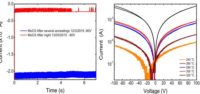
Another phenomenon that can be observed in these samples concerns the lifetime of the sample conductivity after annealing. It was noticed that these samples lose their conductivity a day after the annealing and even with the contact being established. In Fig. 5.7 I(V)-t curve, can be observed that for the same applied voltage, of -90 V, the sample current suffered a decrease of 86% 12 hours after being annealed . The samples recover to an insulating state although it would still have a slightly higher conductivity than the unannealed sample.
-100 -50 0 50 100
-3 -2 -1 0 1 2 3 Cu rr en t ( x 10
-7 A
)
Voltage (V)
Figure 5.7 - I(V)-t curve Left: sample with contacts loose conductivity one day after being annealed. Right: test of the influence of temperature of annealing on the conductivity of the con-tacted sample
A logarithmic scale was applied to the I-V plots of annealing tests performed for increasing temperatures (Fig. 5.7 right). The current is increasing with increasing anneal-ing temperature and the contact become better as evidenced in the lower noise and more symmetric curves.
Figure 5.8 – I-V test of the influence of temperature of annealing in the conductivity of the non-contacted sample
In order to understand if this was due to the presence of indium, where it could have evaporated during the RTA process and then deposited over the sample, the same tests were performed in non-contacted samples using tungsten tips (See Fig. 5.8). The same behavior was measured showing that annealing must alter the material itself and
0 2 4 6
-2.0 -1.5 -1.0 -0.5 0.0 Cu rr en t ( x 10
-7 A
)
Time (s)
MoO3 After several annealings 12/3/2015 -90V MoO3 After night 13/03/2015 -90V
-100 -80 -60 -40 -20 0 20 40 60 80 100
10-7 10-6 10-5 Cu rr en t (A)
Voltage (V)
240 °C 260 °C 280 °C 300 °C 320 °C-100 -75 -50 -25 0 25 50 75 100
1.0 1.5 2.0 2.5
After annealing, 310 C, 240 sec 2 h after annealing
day after annealing
Curr
ent
(
x 10
-7 A
)
not only the contact. The recovery behavior took place again, decreasing about 75% from the maximum current measured for 100V.
The creation of oxygen vacancies during annealing may explain such behavior since they are known to be donors in most metal oxides. On the other hand, the slow recovery of the initial state may point to adsorption effects at the surface, meaning oxy-gen molecules or other adsorbents are returning to the surface of molybdenum oxide. [6].
The reason behind this different reaction between gallium oxide and molybdenum trioxide crystals, might be attributed to the crystal’s production temperature where gal-lium oxide crystals were produced at approximately 1500 ºC and molybdenum trioxide flakes were produced at approximately 800 ºC.
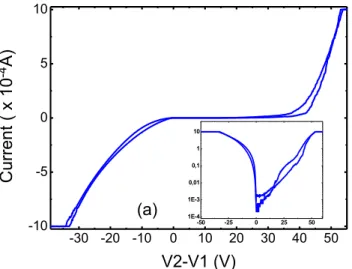
For the case of Gallium oxide crystal flakes, the best work setup found was with the silver ink from circuit works®.
Figure 5.9 - I-V curve for a gallium oxide sample with silver contacts
The silver ink is liquid and solidifies at room temperature. This ink was directly deposited on top of the gallium oxide crystals and the typical I-V curves obtained can be seen in Fig. 5.9. No annealing’s were performed in this devices since the ink is polymeric and evaporates.
A current limitation was set in order to preserve the contacts and the material. The limit settled was 1 mA and corresponds to the saturation lines that take place when the volt-age is around -30 V or 50 V.
A logarithmic scale has been proved useful to compare device polarizability answer to direct bias and to reverse bias, as can be seen in the inset in Fig. 5.9. If the contacts were equal the curve would be symmetric and as can be observed, the contacts are not equal.
-30 -20 -10 0 10 20 30 40 50
-10 -5 0 5 10
-50 -25 0 25 50
In the following paragraphs a possible explanation about this phenomenon will be giv-en.
Being contact nº1 at zero Volt, when the applied tension in contact nº2 is negative, the conventional current flows from contact nº1 to contact nº2, and it encounters a re-sistance different than when it flows from contact number 2 to number 1. This means that one contact is offering more resistance to the passage of current than the other and this resistance depends on the direction of the current flow (as expected for a Schottky diode).
Figure 5.10 - I-V curve situations where the current flows from contact nº1 to contact nº2 and vice-versa.
In Fig. 5.10 it is represented in yellow the experimental values for which the
cur-rent flows from contact nº1 to nº2, and in red it’s represented the opposite path. This means that for each yellow path, the 1st contact is directly polarized and the 2nd contact is
reversely polarized. For the red lines the opposite is true.
So it can be observed that the contact number one is offering more resistance when re-versely polarized.
When the contact is directly polarized the current flows without much effort from the metal to the semiconductor when the potential difference is high enough to over-come the Schottky barrier (thermionic effect). However, if in this circuit the current flows from the semiconductor to the metal , this contact is reversely polarized and the energy necessary to overcome it is not only the one given by thermionic effect but is also due to field effect emission [3].
We can conclude so far that to make contact with Ga2O3, silver ink is a good
solu-tion because it is relatively cheap (at least half the price of a silver sheet/wire and a third of the price of a gold leaf/thread) and it is also easy to handle.
The contacts were stable, adhering, which led to reproducible I-V curves with
low--0.4 -0.2 0.0 0.2 0.4
-10 -5 0 5 10 2 2 2 1 1 1 C urrent ( x 10
-4 A
)
The same device configuration was developed for exfoliated samples and for nan-owires and proved to be a good setup for future irradiation studies, although some thermal evaporation of metal contacts had been done they prove to fail in terms of the crystals endurance for successive studies, since thin layers with hundreds of nanometers did not present the robustness needed for the study of these materials.
To further understand the conduction mechanism of the samples, some tests were performed taking into account the three possible spatial orientations as shown in Fig. 5.11 for gallium oxide samples with silver contact.
Figure 5.11 - Schematic of the three contact configurations performed with silver (repre-sented in grey) and Ga2O3 (represented in black) and respective I-V curves for a) bulk
conductivi-ty along the a crystal axis b) conductiviconductivi-ty in the c direction crystal axis and c) conductiviconductivi-ty in the direction b crystal axis.
For I-V a) and b) curves correspondent to the geometry defined below each plot, were smoothed (red solid line) in order to understand better the I-V curves despite the high noise level.
For the cases represented in a) and b), in Fig. 5.11, the currents measured are of the order of 10−7 A, and for the case represented in c), the current measured achieves values three orders higher than for the first two contact configurations. Also, a) and b), show a lot of noise and hysteresis, were in c) this phenomena is smaller. The contacts were pro-duced in the same manner, so the conductivity along the axis given by a) and b) are neg-ligible relatively to the axis given by c).
in Chapter 3, were three different electronic distributions can be observed in the different crystal orientations.
For the case of molybdenum oxide samples, a similar procedure with indium con-tacts was made and in the c axis it showed increased conductivity while for the conduc-tivity along the bulk and the a axis direction it showed no conducconduc-tivity, however, these measurements were not conclusive because the samples were highly damaged during the measurement due to their high level of brittleness.
The devices that ultimately showed better working conditions (less noise, few hys-teresis, stable and reproducible measurements) and used to perform the irradiation stud-ies are given in Table 5.1.
Table 5.1 – Devices produced and used for irradiation tests
Sample Characteristics Tests Realized
Devices Studied Dimensional
Limit Dimension Contacts Substrate
I(t) UV(air)
Proton
(2nA)
(Vacuum)
Vacuum
Test
Voltage Applied (V)
𝐆𝐚𝟐𝐎𝟑
Flakes (2D) -
non irradiated
sample
[0.83 x 0.21 cm] silver ink kapton
tape -10 -10
Flakes (2D) -
irradiated
sam-ple
[0.74 x 0.18 cm] silver ink kapton
tape -10 After pro-ton irradia-tion: -10 -10
Nanowires(1D) [900 nm x 800 um];
thickness =900nm silver ink -10 60
𝐌𝐨𝐎𝟑
Flakes (2D) [92.3 µm x 246 µm];
thickness = 10 µm indium
kapton
tape -10 -10
Nanoplates
(2D)
[340 µm x 800 µm];
thickness = 5 µm
indium with
traces of lead
and copper
Radiation -Matter Interaction
Radiation is the emission of energy as electromagnetic radiation, such as heat radi-ation and X-rays, or the emission of energy as moving subatomic particles, in particular high-energy particles, which can cause ionization of the medium. In this work, we are particularly interested in phenomena using ultra-violet (UV) radiation and energetic ion beams.
6.1 Electromagnetic radiation-matter interaction
Several phenomena can occur during electromagnetic radiation-matter interaction; namely, absorption, photoelectric effect, Compton Effect, pair production among others, dependent on the photons energy and on the atomic number and electronic density of the material [32]
In absorption, the medium will absorb some of the energy carried by the electro-magnetic wave attenuating the intensity of incident beam as it passes through the mate-rial. The intensity of the incident radiation decreases exponentially with distance trav-elled in the material and it is described by the Lambert-Beer law:
𝐼(𝑙)
𝐼
0= 𝑒
−4𝜋𝑘𝜆 𝑙𝑐
(6.1)
Where k is the extinction coefficient, 𝜆 is the wavelength of the radiation used, l is the path length made by radiation beam and c the concentration of the absorbent sub-stance in the medium. To the energy carried by the electromagnetic field, there is associ-ated a photon of energy:
𝐸
𝑝ℎ= ℎ
𝜆
𝑐
(6.2)In a semiconductor, an electron in the valence band absorbing the energy of the photon can acquire enough energy to jump to the conduction band, if the photon energy is equal to or higher than the bandgap. When the conduction band has a minimum at another position than zero for the k vector of the Brillouin Zone, i.e. in an indirect-gap semiconductor, a higher energy than EG is required for this transition or an additional
phonon needs to be absorbed by the electron.
When an electron is excited to the conduction band, a hole is also created in the va-lence band. After excitation with electron can either recombine directly with a hole in the valence band or it can form an exciton. In this case, the electron is attracted to the hole and a bound state is created where both particles revolve around their center of mass. This attraction diminishes the energy difference between the electron and hole levels fall-ing slightly below EG.
Also free carriers can absorb radiation without being excited to another band due to available quantum states more favorable in the same band. These are called intraband transitions. When semiconductors have impurities, those can influence the degree and type of absorption. There can be shallow impurities whose energy levels are closer to the conduction band and deep impurities that capture the charge carriers and change the conductivity of the material.
6.2 Ion-Solid Interaction
In case of an energetic ion-beam, the particles traveling through the material will transfer some of their energy to the material (nuclei or electrons) by elastic or inelastic collisions that can result in crystal structure breakups or electronic excitation of the ma-terial’s atoms, giving rise to changes in the electronic properties. In this work, we focus on the electronic changes since our main purpose is to study the conductivity properties and behavior. Due to the charge of the particles, the interaction ion-material is of Cou-lombic nature (electric nature).
Particles will go through the material, depositing energy along their path and if this medium is sufficiently thick, these particles will be totally decelerated and their en-ergy totally absorbed by the medium.
6.3 The Stopping Power
The energy transferred by one particle per unit path length in the medium is called the stopping power-dT/dx. Firstly described by Bohr, the stopping power was written in terms of the kinematic factor, which takes contribution of the mass and electronic charge per unit volume of the medium and the velocity of the incident particle [22]. But a quan-tum mechanical and statistical approach was needed and Hans Bethe provided it con-sidering the mean excitation potential of the atom and another function for the contribu-tion of velocity for the stopping power [22]. This formula also allows relativistic concepts to be included by corrections to the velocity term. However, the mean excitation poten-tial is not given by a single theory, because there would have to be knowledge of every ground and excited state. In these terms, Felix Bloch showed that the mean excitation potential can be approximated by statistical methods [22]
Those theories combined, will describe the decreasing energy of an ion when pass-ing a medium, accordpass-ing to the Bethe-Bloch formula. Adding the Bragg’s Rule for com-pounds, total stopping power can be described by the linear combination of the stopping powers of individual elements.
Because of the large amount of unknown variables for calculations of each materi-als stopping power values, simulations using Monte Carlo algorithm have been exten-sively used to preview the right stopping power characteristics for a large amount of ma-terials and the values simulated are not far from those calculated with an estimated 2% error.
Figure 6.1 - Typical Bragg Curve represented as a function of the distance accomplished for a light energetic particle in a heavy matrix.
transfer is maximum, and the maximum penetration depth of the protons can be esti-mated from the stopping power curves.
Figure 6.2 - Comparison between nuclear (red data and red scale) and electronic stopping power (blue data and blue scale) for protons in gallium oxide.
In Fig. 6.2 nuclear and electronic stopping power curves, for gallium oxide irradi-ated by a proton beam, as a function of the energy of the beam are represented. The curves were obtained using the Stopping and Range of Ions in Matter (SRIM) software. As one can observe the electronic contribution is much more relevant than the nuclear contribution for the case of 2 MeV beam. The peak means that the energy for which the particle loses more energy to the material is at 0.1 MeV.
6.4 Simulation of Proton Irradiation Profiles
Since the materials investigated in this thesis are being studied in terms of being sensors of irradiation, ion impact profiles were studied.
with hydrogen ion beam, where the plots correspond to the experimental and simulation (black solid line) data for many values of beam energy [33].
For 2 MeV proton beam in gallium and molybdenum it is shown that a maximum of 10% uncertainty is expected for the hydrogen ion beam.
However this comparison is just relative to the heaviest elements in the crystal structure that are studied in this work, because the crystals were not found in the litera-ture and since stopping power depends proportionally on the atomic number (Bethe-Block equation) it seems an acceptable correlation to be made).
However, TRIM does not take into account inhomogeneous surfaces, nor does it take into account laterally asymmetric samples [34]. For instance, in Fig. 6.4 the errors that are being made if simulations for nanostructures are being made assuming a bulk structure instead of the real geometry of a nanostructure can be observed.
Figure 6.4 - Comparing SRIM simulation assuming a bulk geometry (left) and using the program Ion Range And Damage In Nanostructures (Iradina) [34] assuming the correct geometry of a nanowire.
If the simulations are being made in the SRIM ambient, they will not take into ac-count the geometry of the sample, like for case of nanowires with diameters of hundreds of nanometers as used in this study.
So for nanostructures, irradiation profiles had to be simulated using Iradina (see Fig. 6.4) and bulk structures by Transport of Ions in Matter (TRIM).
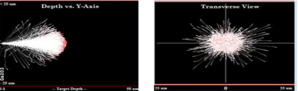
Figure 6.5 - TRIM simulation showing the ion tracks with depth and in transverse view for a 2 MeV proton beam in Ga2O3
Figure 6.6 -Total displacements of both gallium and oxygen caused by the passage of the beam; Ionization profile in gallium oxide by the electronic collisions with the ion beam, distribu-tion of protons in gallium oxide.
For the Ion Distribution in the gallium oxide layer, for a 2 MeV proton beam, it will be with a higher probability totally stopped by the target atoms at the depth of the Bragg peak. Simulations yield a projected range of 22 m and a straggling of 7890 Angstroms.
Figure 6.7 - TRIM simulation showing the ion tracks with depth and in transverse view for a 2 MeV proton beam in MoO
Figure 6.8 - Ionization profile of molybdenum oxide caused by the passage of the 2MeV proton beam in molybdenum oxide; Total Displacements of both molybdenum and oxygen, Pro-ton distribution in molybdenum oxide.
For the Ion Distribution in the molybdenum trioxide layer, for 2 MeV protons, simulations yield a projected range of 30.5 m with a straggling of 8089 Angstrom near the Bragg Peak.
component of the stopping power is making the displacements of target atoms through elastic collisions between the target nuclei and the ions.
On average, for each proton being bombarded into the sample, 29 atoms are being displaced.
Simulations for an irradiation of a nanowire of Ga2O3 (radius of 900 nm and
irradi-ated from the side facet) by a 2 MeV proton beam were performed using the Iradiana code. Results are shown in Fig. 6.9 where the images represent the amount of energy de-posited in the nanowire by inelastic electronic energy loss and by the energy loss by re-coils.
It is seen that the electronic energy deposition is homogeneous throughout the nanowire thickness and that very few displacements occur (see Fig.6.10). It makes sense that not many effects are observed in terms of displacements since the nanowire has a radius of 900 nm and the range for 2 MeV protons in gallium oxide is 23 micrometers.
Figure 6.9 - Ionization profile of the nanowire where the beam enters the nanowire perpendicular to the x-axis.
Figure 6.10 - Displacements of gallium and oxygen along the x-y plane of a 900 nm diame-ter Ga2O3 nanowires irradiated with 2 MeV protons.

![Figure 6.3 - SRIM simulation plots for stopping power for hydrogen ion irradiation for a gallium target (top left plot) [47] and for molybdenum target (top right plot) [48]](https://thumb-eu.123doks.com/thumbv2/123dok_br/16539194.736657/55.892.136.807.366.784/figure-simulation-stopping-hydrogen-irradiation-gallium-target-molybdenum.webp)
![Figure 6.4 - Comparing SRIM simulation assuming a bulk geometry (left) and using the program Ion Range And Damage In Nanostructures (Iradina) [34] assuming the correct geometry of a nanowire](https://thumb-eu.123doks.com/thumbv2/123dok_br/16539194.736657/56.892.161.735.289.543/comparing-simulation-assuming-geometry-nanostructures-iradina-assuming-geometry.webp)