c
Copernicus GmbH 2003
Advances in
Radio Science
Exploration of dual supply voltage logic synthesis in state-of-the-art
ASIC design flows
T. Mahnke1, W. Stechele1, M. Embacher2, and W. Hoeld2
1Institute for Integrated Circuits, Technical University of Munich, Germany 2National Semiconductor GmbH, Fuerstenfeldbruck, Germany
Abstract. Dual supply voltage scaling (DSVS) for logic-level power optimization at the has increasingly attracted at-tention over the last few years. However, mainly due to the fact that the most widely used design tools do not support this new technique, it has still not become an integral part of real-world design flows. In this paper, a novel logic syn-thesis methodology that enables DSVS while relying entirely on standard tools is presented. The key to this methodology is a suitably modeled dual supply voltage (DSV) standard cell library. A basic evaluation of the methodology has been carried out on a number of MCNC benchmark circuits. In all these experiments, the results of state-of-the-art power-driven single supply voltage (SSV) logic synthesis have been used as references in order to determine the true additional benefit of DSVS. Compared with the results of SSV power optimization, additional power reductions of 10% on aver-age have been achieved. The results prove the feasibility of the new approach and reveal its greater efficiency in compar-ison with a well-known dedicated DSVS algorithm. Finally, the methodology has been applied to an embedded micro-controller core in order to further explore the potentials and limitations of DSVS in an existing industrial design environ-ment.
1 Introduction
The total power dissipation of digital CMOS circuits is com-posed of static and dynamic components. While static power contributes significantly to the total power in certain applica-tions that are inactive for long periods of time, it is still dom-inanted by dynamic power in the majority of applications.
The dynamic powerPdyn is composed of the capacitive
powerPcap and the short-circuit powerPsc. The capacitive
power Pcap is due to currents charging or discharging the
node capacitances and can be written as
Pcap =α01·fclk·Cnode·VDD2 , (1)
where α01 is the switching activity, fclk is the clock
fre-quency,Cnodeis the node capacitance, andVDD is the sup-Correspondence to:T. Mahnke ([email protected])
ply voltage. AlthoughPcap usually accounts for the largest
portion of the total dynamic power, Psc must not be
ne-glected. The short-circuit power is caused by currents flow-ing through simultaneously conductflow-ing n- and p-channel transistors. A first-order approximation ofPscis
Psc =α01·fclk·(β/12)·tT ·(VDD−2Vt)3 , (2)
whereβ is an effective transconductance,tT is the input
sig-nal transition time andVt is the threshold voltage.
A very efficient means of reducingPdynis supply voltage
scaling. However, since gate delay increases with decreasing
VDD, globally loweringVDDdegrades the performance. At
the logic level, dual supply voltage scaling (DSVS) can be used for loweringVDDonly in non-timing-critical paths, thus
keeping the overall performance constant (Chen at al., 2001; Usami and Horowitz, 1995; Usami et al., 1998a,b; Yeh et al., 1999b).
In our work, we modified an existing power-driven logic synthesis methodology such that DSVS is supported in ad-dition to state-of-the-art optimization techniques. This ap-proach enabled us to carry out DSVS in a conventional logic synthesis environment, while all previously published work required proprietary tools that comprise dedicated DSVS al-gorithms. In our discussion of the experimental results, we use the results of state-of-the-art power-driven single supply voltage (SSV) logic synthesis as reference values in order to reveal the true additional benefit of DSVS.
The remainder of the paper is structured as follows. In Sect. 2, a short overview of state-of-the-art logic-level power optimization is given. In Sect. 3, we introduce the DSVS technique. Our novel power-driven logic synthesis method-ology is described in Sect. 4. Results of the optimization of a number of benchmark circuits and an embedded microcon-troller are presented in Sects. 5 and 6. Finally, we provide concluding remarks.
2 State-of-the-art in power-driven logic synthesis
In conventional logic synthesis methodologies,Pdyncan
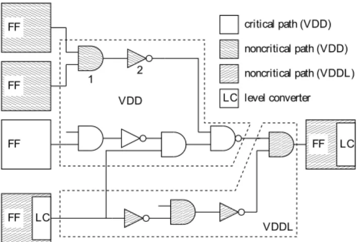
LC FF
LC FF FF
FF
FF
2 1
VDDL VDD LC level converter
noncritical path (VDDL) noncritical path (VDD) critical path (VDD)
Fig. 1.A typical dual supply voltage (DSV) circuit structure.
Down-sizing primarily aims at reducingCnode and, thus,
Pcap by using smaller slower cells in non-timing-critical
paths, but also reduces short-circuit currents and, hence,Psc
at the sized gates. On the other hand, increasing the size of a gate shortens the signal transition timetT at its output, which
in turn reducesPscat the gates driven by the sized cell.
Alter-natively, extra buffers can be inserted at heavily loaded nodes in order to shortentT. Equivalent pin swapping takes
advan-tage of the fact that functionally equivalent input pins of logic gates often exhibit different power characteristics. With pin swapping, high activity nets are connected to power-efficient input pins with priority.
In our experiments, we made extensive use of the above mentioned techniques when we created the SSV reference designs.
3 Dual supply voltage scaling (DSVS)
The purpose of DSVS is to reduce the supply voltage for gates in noncritical paths from the nominal valueVDD to a
lower valueVDDL(Chen at al., 2001; Usami and Horowitz,
1995; Usami et al., 1998a,b; Yeh et al., 1999b). Figure 1 il-lustrates a typical (DSV) circuit structure. In DSV circuits, low voltage cells must not directly drive high voltage cells. Otherwise, quiescent currents occur at the driven gates. This is the reason why gates 1 and 2 in Fig. 1 are operated atVDD
although they are part of a noncritical path. Level-converting cells can be inserted where transitions fromVDDLtoVDDare
required (Usami et al., 1998a). However, these cells intro-duce additional delay and cause power and area overhead. In order to minimize this overhead, we enable level conversion only at the input and output nodes of combinational blocks as depicted in Fig. 1.
Other difficulties are the distribution of two supply volt-ages across the chip and the layout synthesis. One possible solution to these problems is placing low and high voltage cells in separate rows. This can be realized on the basis of conventional cell layouts but requires proprietary tools (Us-ami et al., 1998a). Another possibility is the use of two
sep-arate power rails forVDD andVDDL in each row. This
re-quires modification of the layouts of all cells. However, low and high voltage cells can then be mixed within rows and, hence, placement and routing can be carried out using stan-dard tools (Yeh et al., 1999a).
4 Dual supply voltage logic synthesis methodology
4.1 Tools for dual supply voltage scaling
All known approaches to DSVS are based on dedicated algo-rithms (Chen at al., 2001; Usami and Horowitz, 1995; Usami et al., 1998a,b; Yeh et al., 1999b), and not one of these algo-rithms has been integrated into standard tools yet. However, DSVS can be carried out without the need for any dedicated algorithm which is evident from the following simple argu-ments. At the logic level, standard cells are distinguished only by functionality, delay, power, input capacitance and area. Typical cell-library-based gate sizing algorithms, such as the one presented by Coudert (1997), revert only to these properties when picking cells that implement certain func-tionalities while minimizing the power consumption subject to delay constraints. Knowing that a reduction of the supply voltage for a cell changes only its delay and power, we con-clude that cell-library-based gate sizing algorithms should be able to handle functionally equivalent low and high voltage cells in the same way as cells of different size. Cell-library-based gate sizing algorithms are readily available with stan-dard tools such as Synopsys’ Power Compiler (SPC). Thus, instead of developing yet another dedicated DSVS algorithm, we forced SPC to perform DSVS along with gate sizing. For-tunately, the tool allows input and output pins of cells to be classified such that only pins of the same class will be inter-connected. While this feature was originally introduced for coping with high I/O and low core voltages, it also allows us to solve the level conversion issue discussed in Sect 3. Power analysis was carried out at the logic level using Synopsys‘ Design Power (SDP).
4.2 Design flow and optimization strategy
timing−driven synthesis
disable VDDL & LC original design
SSV implementation (timing−optimized)
VDDL & LC enable
SSV implementation (power−optimized)
gate level simulation
delay−constrained power−driven synthesis
implementation (power−optimized)
DSV DSV synthesis library
STEP 2 STEP 3
STEP 1
STEP 2
α01
Fig. 2.Design flow comprising DSVS in addition to state-of-the-art power optimization.
4.3 Dual supply voltage synthesis library
The key to DSVS exploiting gate sizing algorithms is a suitably modeled standard cell library. We developed a DSV synthesis library from a commercial library realized in 0.25µm CMOS and characterized at supply voltages of 1.8V and 2.5V. It has been shown elsewhere that for a given
VDDan optimalVDDLexists (Chen at al., 2001; Usami and
Horowitz, 1995; Usami et al., 1998a,b). On the other hand, the optimal choice ofVDDL depends largely on the circuit
to be optimized (Chen at al., 2001). Note that in our experi-ments we always used the voltage levels given above, which were defined by the library vendor, and forwent the costly procedure of determining an optimal voltage pair for each circuit, which was used by Chen at al. (2001) and Usami et al. (1998a).
The DSV library contains inverters, buffers, (N)ANDs, (N)ORs, X(N)ORs and D-flip-flops in up to five different sizes each. For each cell, high and low voltage synthesis models are provided and a level-converting flip-flop (DF-FLC) similar to the one used by Usami et al. (1998b) was included in order to enable level conversion at the inputs and outputs of combinational blocks as described in Sect. 3. Fur-thermore, we classified the input and output pins of all cells such that ouput pins of low voltage cells are not allowed to drive input pins of high voltage cells.
For SDP to properly calculate the power consumption in the presence of two supplies, we modeled Pdyn for each
cell individually. While cell-internal look-up tables are nor-mally used for modeling only cell-internal dynamic power (Ackalloor and Gaitonde, 1998), we used them for model-ing all the dynamic power. For a more detailed discussion of tool-specific DSV library modeling issues see Mahnke et al. (2002a).
The 0.25µm CMOS library was used for implementing MCNC benchmark circuits (see Sect. 5). For the implemen-tation of the embedded microcontroller (see Sect. 6), we de-veloped another DSV library based on National
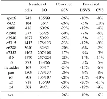
Semiconduc-Table 1.Results of the optimization of combinational benchmarks. Col. 2/3: circuit complexity. Col. 4: power reduction due to SSV power optimization. Col. 5/6: additional power reduction due to the use of a second supply voltage
Number of Power red. Power red.
cells I/O SSV DSVS CVS
apex6 742 135/99 -26% -10% -8%
c432 184 36/7 -26% -3% ±0%
c880 416 60/26 -22% -12% -4%
c1908 275 33/25 -30% -7% -6%
c3540 1077 50/22 -25% -5% -1%
c5315 1413 178/123 -23% -12% -9%
c6288 3040 32/32 -20% -6% -2%
c7552 1462 207/108 -17% -9% -5%
i10 1879 257/224 -28% -14% -11%
i5 373 133/66 -28% -5% -5%
my adder 169 33/17 -24% -13% -6%
pair 1509 173/137 -26% -9% -8%
rot 708 135/107 -28% -13% -10%
x3 718 135/99 -28% -20% -11%
x4 368 94/71 -35% -12% -9%
avg. – -26% -10% -6%
tor’s 0.18µm CMOS technology. This library contains high voltage (1.8V) and low voltage (1.3V) synthesis models of all logic cells that exist in the original SSV library. Further-more, high voltage, low voltage and level-converting scan-flip-flops are provided in three different sizes each.
5 Evaluation of the methodology
We applied our methodology to MCNC benchmark circuits (CBL, 2002) subject to reasonably strict delay constraints. In the following discussion, we use the results of state-of-the-art power-driven SSV logic synthesis (see Sect. 2) as ref-erence values in order to reveal the true additional benefit of DSVS. In this paper, we restrict the discussion to a selec-tion of combinaselec-tional benchmark circuits. For the results of the optimization of sequential benchmark circuits and for a more detailed discussion of delay constraints see Mahnke et al. (2002b).
We optimized the power consumption of 15 combinational MCNC benchmark circuits, firstly, using the state-of-the-art methodology for power-driven logic synthesis (SSV opti-mization, STEP 1 and STEP 2 in Fig. 2) and, secondly, using our DSVS methodology (STEP 3). The results are summa-rized in Table 1. Column five shows the advantage of our methodology over SSV power optimization. On average, the final power consumption was 10% lower if DSVS was used. In the best case, the improvement was 20%.
power optimization using the established SSV methodology first, followed by CVS. Column six of Table 1 shows that the
additional power reduction due to CVS was only 6% on aver
-age and only 11% in the best case. This is significantly less than the additional power reduction that we achieved using our DSVS methodology.
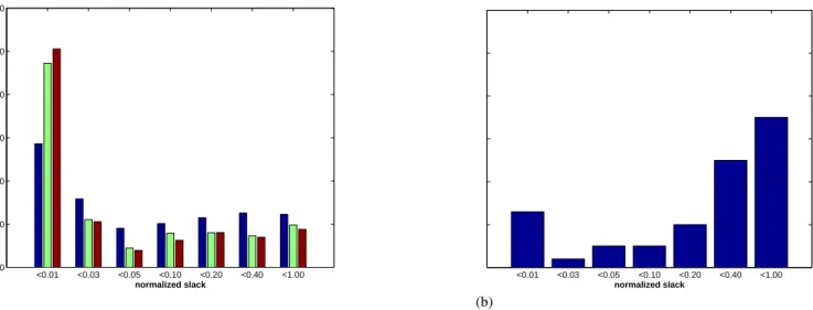
The fact that we observed less power reduction than other researchers reported can be explained on the basis of a slack distribution analysis. We performed static timing analysis on a number of MCNC benchmark circuits after timing-driven synthesis, after SSV power optimization and after DSV power optimization, thereby assigning to every gate in the netlists the slack of the longest path that contains the re-spective gate. The results are given in Fig. 3a. In this bar graph, the slack normalized to the delay of the critical path and devided into seven intervals is shown on the horizontal axis. The normalized slack values contained in the figure de-note the upper limits of the intervals. There are three bars associated with each slack interval. In each group of three bars, the left bar corresponds to the situation after timing-driven synthesis, the middle bar represents the results of SSV power optimization and the right bar describes the situation after DSV power optimization. The height of each bar is proportional to the number of cells that have a slack in the respective interval.
A similar analysis was carried out by Chen at al. (2001) on their selection of MCNC benchmark circuits after timing-driven synthesis. From the results, which are reproduced in Fig. 3b, Chen et al. concluded that there was a large potential for power reduction using the DSVS technique because of the large number of noncritical cells.
However, from a comparison of the two bar graphs, it is evident that, after timing-driven synthesis (see left bars in Fig. 3a), the benchmark circuits were more timing criti-cal in our work. Consequently, there was less potential for power-delay-tradeoff. This discrepancy must be accredited to the capabilities of the tools used for timing-driven syn-thesis. Moreover, the extensive use of SSV power optimiza-tion techniques, particularly the use of gate sizing, signifi-cantly increased the number of critical cells (see middle bars in Fig. 3a) and, hence, reduced the optimization potential even further. As a result, the increase of the number of crit-ical cells during DSV power optimization (see right bars in Fig. 3a) and the additional power reduction was compara-tively small.
6 Application to an embedded microcontroller
We ported our methodology to National Semiconductor’s standard ASIC design environment and applied it to the 16-bit CompactRISCTM (CR16) microprocessor core module. The CR16 is usually implemented as part of embedded mi-crocontroller systems, which typically include a numerous peripheral modules such as bus controllers, timers, inter-rupt controllers, memory controllers, memory (e.g. cache, RAM, ROM) and a variety of interfaces (e.g. USB, I2C,
Mi-crowire). Recently developed applications comprising such microcontrollers are a keyboard and power management con-troller for notebooks and information appliances, DECT and Bluetooth baseband controllers, and a digital color image processor.
In our work, we synthesized the CR16 core module to Na-tional Semiconductor’s 0.18µm CMOS technology for op-eration at a nominal supply voltage of 1.8V. The timing-driven synthesis was performed subject to the strictest tim-ing constraints. For the DSV power optimization, the second supply voltage was set to 1.3V. Some important character-istics of our experimental CR16 implementation are a clock frequency of 100 MHz and a complexity of approximately 14000 cells. Following National Semiconductor’s common standards for CR16 implementations, the module was pre-pared for the scan test method and gated clocks were used for dynamic power reduction. In order to make scan testing of the DSV implementation possible, we developed level-converting flip-flops that support the scan test method.
In a first set of experiments, we performed timing-driven synthesis followed by SSV and DSV power optimization as-suming a high voltage clock signal. The results show that this module had only limited optimization potential. The SSV power optimization, for instance, reducedPdynby only 11%
and DSVS yielded only 4% additional power reduction. In a second set of experiments, we extended the voltage scaling approach to the clock network in order to achieve additional power reduction and, thus, improve the optimiza-tion results. For this purpose, we disabled the use of high voltage flip-flop cells, so that the SSV implementations con-tained only level-converting flip-flops and the DSV imple-mentations contained only low voltage and level-converting flip-flops. Under these circumstances, the signal level in the clock network could be safely reduced fromVDDtoVDDL.
The substitution of conventional high voltage flip-flops with their level-converting counterparts generally creates de-lay and power overheads, since the level-converting cells are slower and consume more cell-internal dynamic power. In the case of the CR16 core module, the performance penalty was only 2% while the power overhead was 5%. On the other hand, the large number of level converters improved the ef-ficiency of DSVS in the logic, i.e. the dynamic power was reduced by 7% instead of 4%. This partially compensated for the power overhead.
<0.01 <0.03 <0.05 <0.10 <0.20 <0.40 <1.00 0
10 20 30 40 50 60
normalized slack
no. of gates in %
<0.01 <0.03 <0.05 <0.10 <0.20 <0.40 <1.00
normalized slack
(a) (b)
Fig. 3.Slack statistics(a)for a subset of ten combinational benchmark circuits implemented and optimized using the methodology presented in this paper, and slack statistics(b)for 16 combinational benchmark circuits published by Chen at al. (2001).
7 Conclusions
We have shown that DSVS can be carried out exploiting existing gate sizing tools, provided that a suitably modeled
DSV standard cell library exists. The required DSV sy
nthe-sis library file can easily be created from two conventional SSV libraries. The only costly task remaining is the design of the level-converting flip-flop cells, which, of course, is re-quired by any DSV design methodology. Consequently, our methodology can be adopted with a modicum of effort.
A slack distribution analysis has shown that timing-driven synthesis using standard synthesis tools usually generates netlists that contain a large number of timing-critical cells. Moreover, the number of critical cells further increases if state-of-the-art SSV power optimization is used. Therefore, the true additional benefit of DSVS is smaller than claimed by other researchers. On average, we observed an additional power reduction of 10%.
For a comparison with related work, the selection of cir-cuits, the quality of the timing-driven synthesis, the technol-ogy and the library, the supply voltages and the use of state-of-the-art power optimization techniques had to be taken into account. For this reason, we implemented a previously pub-lished DSVS algorithm and applied it to benchmark circuits within our synthesis environment. The results revealed a greater efficiency of our approach.
Our methodology supports clock voltage scaling for power reduction in the clock network. The performance penalty due to level-converting flip-flops in critical paths was small in the case of the CR16 microprocessor core. However, clock voltage scaling turned out to be inefficient for a design that makes extensive use of gated clocks.
References
Ackalloor, B. and Gaitonde, D.: An overview of library characteri-zation in semi-custom design, IEEE Custom Integrated Circuits Conf., 305–312, 1998.
Chen, C., Srivastava, A., and Sarrafzadeh, M.: On gate level power optimization using dual-supply voltages, IEEE Trans. VLSI Sys-tems, 9, 616–629, 2001.
Collaborative Benchmarking Laboratory (CBL), LGSynth93 benchmark set used in conjunction with 1993 MCNC Interna-tional Workshop on Logic Synthesis, http://www.cbl.ncsu.edu, June 2002.
Coudert, O.: Gate sizing for constrained delay/power/area opti-mization, IEEE Trans. VLSI Systems, 5, 465–472, 1997. Mahnke, T., Embacher, M., Stechele, W., et al.: Power optimization
through dual supply voltage scaling using Power Compiler, Proc. European Synopsys Users Group Meeting, 2002a.
Mahnke, T., Stechele, W., and Hoeld, W.: Dual supply voltage scal-ing in a conventional power-driven logic synthesis environment, Proc. Int. Workshop on Power and Timing Modeling, Optimiza-tion and SimulaOptimiza-tion (PATMOS), 146–155, 2002b.
Synopsys Inc.: Design power and power compiler technology backgrounder, 1998, http://www.synopsys.com/products/power/ power\bkg.html, 2001.
Usami, K. and Horowitz, M.: Clustered voltage scaling technique for low-power design, Proc. Int. Symp. Low-Power Design, 3–8, 1995.
Usami, K., Igarashi, M., Minami, F., et al.: Automated low-power technique exploiting multiple supply voltages applied to a media processor, IEEE Journal of Solid-State Circuits, 33, 463–472, 1998.
Usami, K., Igarashi, M., Ishikawa, T., et al.: Design methodology of ultra low-power MPEG4 codec core exploiting voltage scaling techniques, Proc. 35th DAC, 483–488, 1998.
Yeh, C., Chang, M.-C., Chang, S.-C., et al.: Gate-level design exploiting dual supply voltages for power-driven applications: Proc. Design Automation Conf., 68–71, 1999a.