Bernardo Garcia Caetano
Bachelor of Science in Micro and Nanotechnologies Engineering
Study of P(VDF-TrFE) for Structures via
3D Printing
Dissertation submitted in partial fulfilment of the requirements for the degree of
Master of Science in Micro and Nanotechnologies Engineering
Adviser:
Professor Doutor Rui Alberto Garção Barreira do Nascimento
Igreja, Assistant Professor, FCT-UNL
Co-adviser: Professor Doutor Pedro Miguel Cândido Barquinha,
Associate Professor, FCT-UNL
December, 2019
Chair
Prof. Dr Rodrigo Martins
Rapporteurs Prof. Dr Maria do Carmo Lança
Member
Prof. Dr Rui Igreja
iii
Study of P(VDF-TrFE) for Structures via 3D Printing
Copyright ©Bernardo Garcia Caetano, Faculdade de Ciências e Tecnologia, Universidade Nova de Lisboa.
A Faculdade de Ciências e Tecnologia e a Universidade Nova de Lisboa têm o direito, perpétuo e sem limites geográficos, de arquivar e publicar esta dissertação através de exemplares impressos reproduzidos em papel ou de forma digital, ou por qualquer outro meio conhecido ou que venha a ser inventado, e de a divulgar através de repositórios científicos e de admitir a sua cópia e distribuição com objetivos educacionais ou de investigação, não comerciais, desde que seja dado crédito ao autor e editor.
v
“The only true wisdom is in knowing you know nothing.”
vii
Acknowledgements
Com o fim de mais uma etapa educativa e pessoal, utilizo esta página da minha dissertação para agradecer a quem contribuiu para que o meu percurso académico corresse da melhor forma.
Começo por agradecer à Faculdade de Ciências e Tecnologias da Universidade Nova de Lisboa, a grande instituição da qual tenho orgulho em dizer que fiz parte e a qual contribui para a pessoa que sou hoje com as suas condições, docentes e os demais.
De seguida, um agradecimento ao professor Rodrigo Martins e à professora Elvira Fortunato pelo criação e investimento no curso de Engenharia de Micro e Nanotecnologias e nos seus alunos, mostrando total confiança nestes e no seu trabalho. Ainda sem esquecer, um agradecimento ao Departamento de Ciências dos Materiais, CENIMAT e CEMOP e às pessoas que nele trabalham e que me ajudaram não só durante o curso, mas também nesta fase importante da dissertação, com a ajuda na ambientação aos laboratórios e com o bom ambiente nos laboratórios. Um agradecimento ao projeto 1D-Neon pelos materiais e equipamentos financiados no âmbito desta dissertação, sem os quais não seria possível.
Aos professores Rui Igreja e Pedro Barquinha, meu orientador e co-orientador, pelo conhecimento transmitido, apoio e ajuda durante toda esta etapa. Ainda um agradecimento ao professor Carlos Dias pelo seu conhecimento e disponibilidade para me ajudar numa parte tão importante desta dissertação. Antes de mais, quero agradecer em especial aos meus pais por me terem dado a oportunidade estudar a este nível com o apoio logístico, financeiro e pessoal que me deram e que me permitiu chegar onde estou. Ao meu irmão um grande obrigado pela picardia saudável que me fez concluir esta etapa com sucesso.
Quero aproveitar para agradecer a todos os amigos que fiz ao longo do curso e dos quais me vou sempre recordar, deixando algum destaque para a grupeta da festança que inclui o Matinhus Matex, a Pina, o Johny, o Toninho, a Carol, o Freferico, o Mc Big Head, o Dj Rebordation, o Sabinex, o Ricardo dos gafanhotos, o Rolo, o PRIMO Diogo, o não padrinho Nuno, o Neto, o Opinião, a Açoreana, a Mariana, o Ferreira, o Castelo, o Luís, o Renato e outros tantos que quando havia festa lá estavam eles. Ainda agradecer ao Carlos Dias e à Glória pelos mais variados momentos marcantes e divertidos ao longo do curso e ainda ao Chico Matos por ter sido um bom senhorio nas minhas estadias.
Um ainda especial obrigado a 3 pessoas que me marcaram bastante nesta passagem por este curso que são a Marta, o Ramos e o Recife. Foram uma madrinha, padrinho e padrinho adotado cinco estrelas e como muitos não se podem gabar, sempre preocupados, interessados e disponíveis.
Deixo para o fim a Inês, a pessoa que mais aturou o meu mau humor nos meus dias maus e stressantes nos quais tinha sempre as palavras certas para me animar, bem como me aturou nos meus dias bons em que partilhava da minha felicidade quando as coisas corriam bem, quer fosse no âmbito da faculdade ou no âmbito mais pessoal. Agradeço-te pela paciência que tiveste comigo e pelo apoio que foste! Obrigado!
ix
Abstract
This work is focussed on using additive manufacturing (AM) to produce electroactive structures using fused deposition modelling (FDM) and P(VDF-TrFE) as a ferroelectric polymer which will confer electroactive properties to printed structures. The FDM, commonly called 3D printing, was chosen due to its emergence in the industry segment with low-cost production and the capability of projecting prototypes without shape limitations, converting a digital design in a physical object. Beyond these features, the possibility of using functional materials and their properties in the production of sensors and actuators was one of the main reasons for the increased interest in this technology.
The boundaries of 3D printing process were explored during the production in order to obtain a uniform and homogenous thin film. It was used a P(VDF-TrFE) filament that was previously extruded to make possible the use of additive manufacturing process. Subsequently, a commercial conductive PLA filament was used to produce electrodes for the electrical characterization of the electroactive films.
P(VDF-TrFE) films with 65 µm and aluminium electrodes yielded the best results with a pyroelectric coefficient of 3 µC m-2 K-1. The aforementioned sample was used to produce a fully 3D printable
pyroelectric sensor. This sensor was made of P(VDF-TrFE), commercial conductive PLA and conventional PLA. The P(VDF-TrFE) provides electroactive properties, conductive PLA enables the creation of conductive tracks and the conventional PLA gave structural basis to the device.
xi
Resumo
Este trabalho foca-se no uso da fabricação aditiva para a produção de estruturas eletroativas usando a modelagem de deposição fundida (MDF) e o P(VDF-TrFE) como polímero ferroelétrico que confere as propriedades eletroativas às estruturas impressas. A MDF, normalmente chamado de impressão 3D, foi escolhida devido ao seu impacto na indústria com os baixos custos de produção e a capacidade de projetar protótipos sem limitações na forma, convertendo um desenho digital numa peça física. Para além destas características, uma das principais razões para o crescente interesse nesta tecnologia foi a possibilidade de usar materiais funcionais que permitem a incorporação de sensores e atuadores.
De forma a obter um filme fino, uniforme e homogéneo foram testados os limites da impressora 3D durante a produção, usando um filamento de P(VDF-TrFE) previamente extrudido de forma a possibilitar o uso de um processo de fabricação aditiva. Posteriormente, foi usado um filamento comercial de PLA condutor para produzir elétrodos necessários para a caracterização elétrica dos filmes de material eletroativo e conexões eléctricas dos dispositivos.
Os dispositivos com elétrodos de alumínio foram os que mostraram melhores resultados apresentando um coeficiente piroelétrico de 3 µC m-2 K-1 para amostras com 65 µm de espessura. Com
os resultados obtidos, esta configuração foi usada para produzir uma estrutura totalmente impressa que incorpora um sensor piroelétrico. Este sensor é composto por P(VDF-TrFE), PLA condutor comercial e PLA convencional. Neste dispositivo, o P(VDF-TrFE) confere as propriedades eletroativas, o PLA condutor permite a criação de pistas condutoras e PLA convencional dá estrutura ao dispositivo.
xiii
Abbreviations
3D Three dimensional
3DP Three dimensional printing
ABS Acrylonitrile butadiene styrene
AM Additive Manufacturing
AOA One layer film with ironing between two evaporated electrodes of aluminium
a.u. Arbitrary unit
BS Bottom Surface
BTO Barium titanate
COC One layer film with ironing between two conductive PLA electrodes printed separately
CPLA Conductive PLA
DSC Differential Scanning Calorimetry
EAP Electroactive polymers
EDS Energy Dispersive Spectroscopy
EEAP Electronic electroactive polymers
EPAM Electric polling assisted additive manufacturing
FDM Fused Deposition Modelling
FFF Fused Filament Fabrication
FOM Figure of Merit
FTIR Fourier-Transform Infrared Spectroscopy
GPIB General Purpose Interface Bus
HT Hotplate at 155 ˚C
IEAP Ionic electroactive polymers
MFI Melt Flow Index
OLF One layer film
OLFI One layer printed film with ironing
PC Computer
PCOC One layer film with ironing with a printed electrode of conductive PLA and
an conductive PLA electrode printed separately
PLA Polylactide
PVDF Polyvinylidene fluoride
P(VDF-TrFE) Poly(vinylidene fluoride-trifluoroethylene)
RT Room temperature
TG+TG- Trans-gauche-trans-gauche phase
TLPF Two layers pressed film
TS Top Surface
TTT All-trans phase
TTTG+TTTG- All-trans-gauche-all-trans-gauche phase
xv
Symbols
Δt Period of time ΔT Variation of temperature ε0 Vacuum permittivity (8.854 × 10⁻¹² F m-1) εr Relative permittivity ρ Resistivity A Area D Strain constantd33 Induced strain in direction 3 per unit electric field applied in direction 3
Ec Coercive field
Fv Figure of merit for a sensor with a voltage read-out circuit
ip Pyroelectric current
k33 Electromechanical coupling factor
L Length pi Pyroelectric coefficient Pr Remanent polarisation Q Pyroelectric charge R Resistance Rsh Sheet resistance T Thickness Tc Curie temperature tg δ Loss tangent
Vout Output voltage
xvii
Table of contents
Abstract ... ix Resumo ... xi Abbreviations ... xiii Symbols ... xvList of Figures ... xix
List of Tables ... xxi
Motivation and objectives ... 1
Introduction... 3
Fused deposition modelling ... 3
1.1. Working principle of FDM ... 3
1.2. FDM vs Traditional manufacturing techniques ... 3
Extrusion fundamentals ... 4
Functional materials ... 5
3.1. Electroactive polymers ... 5
3.2. Ferroelectric, pyroelectric and piezoelectric materials ... 6
3.3. Ferroelectric polymers ... 6
Fused deposition modelling of ferroelectric polymers ... 7
Materials and Methods……….9
Materials ... 9
1.1. P(VDF-TrFE) ... 9
1.2. Conductive PLA Proto-Pasta ... 9
Sample production ... 9
2.1. Fibre extrusion and filament production ... 9
2.2. 3D Printing of P(VDF-TrFE) film ... 10
2.3. 3D Printing of conductive PLA Proto-Pasta samples to study sheet resistance ... 10
2.4. 3D Printing of conductive PLA Proto-Pasta electrodes ... 10
2.5. Evaporation of aluminium electrodes in P(VDF-TrFE) film... 11
Sample characterization ... 11
3.1. Structural, chemical and morphological characterization ... 11
Electrical characterization ... 11
4.1. Polarisation ... 11
4.2. Measurement of pyroelectric properties ... 12
4.3. Measurement of capacitance ... 13
Device production and experiments ... 13
Results and Discussion……….15
Study of P(VDF-TrFE) for Structures via 3D Printing
xviii
1.1. Study of sheet resistance ... 15
1.2. Characterization of 3D printed electrodes ... 17
P(VDF-TrFE) characterization ... 18
2.1. Morphological characterizations of films ... 18
2.2. DSC characterization of pellet, fibre, two layers pressed film and one layer film with ironing………20
2.3. FTIR characterization of pellet, fibre, two layers pressed film and one layer film with ironing………21
2.4. XRD characterization of pellet, fibre, two layers pressed film and one layer film with ironing………22
2.5. Summary of two layers pressed film and one layer film with ironing characterization .. 23
Sample Characterization ... 23
3.1. Capacitance measurements ... 23
3.2. Polarisation experiments ... 24
3.3. Pyroelectric coefficient and Figure of Merit ... 27
Pyroelectric device experiments ... 29
Conclusion ... 31
References ... 33
Appendices ... 39
A. PVDF and P(VDF-TrFE) molecular structures ... 39
B. Additional information about used materials ... 40
C. Parameters of 3D printing ... 41
D. Rectifying circuit used in polarisation setup ... 42
E. Measurement circuit used during the polarisation ... 43
F. Polarisation process ... 44
G. Measurement of pyroelectric response ... 45
H. Measurement of capacitance ... 46
I. 3D model device ... 47
J. Experimental setup ... 48
xix
List of Figures
Figure 1. Schematic diagram of the FDM process based on [4]. ... 3
Figure 2. Ferroelectric a) phase transition of ferroelectric to paraelectric b) polarization hysteresis from [30]... 6
Figure 3. Used setup in samples polarisation. ... 12
Figure 4. Used setup in measurements of pyroelectric properties of samples. ... 12
Figure 5. Study of sheet resistance with the increasing of the number of layers and comparison between the room temperature dry process of silver conductive ink electrodes with dry of 3 min in hotplate at 155 ˚C. ... 15
Figure 6. Morphological images of the top and bottom surfaces of used sheet resistance samples, with a different number of layers and different dry processes. ... 16
Figure 7. Morphological characterization of the 3D printed electrode. ... 17
Figure 8. SEM-EDS of 3D printed electrodes of a) top surface, and b) bottom surface. ... 18
Figure 9. Morphological characterization of one layer printed film without ironing (OLF). ... 19
Figure 10. Morphological characterization of two layers pressed film. ... 19
Figure 11. Morphological characterization of one layer printed film with ironing (OLFI). ... 20
Figure 12. DSC spectra of P(VDF-TrFE) pellet, fibre, TLPF and OLFI. ... 21
Figure 13. FTIR spectra of P(VDF-TrFE) pellet, fibre, TLPF and OLFI. ... 21
Figure 14. XRD spectra of P(VDF-TrFE) pellet, fibre, TLPF and OLFI. ... 22
Figure 15. Studied configuration a) AOA, b) PCOC and c) COC. ... 23
Figure 16. Curves of capacitance (full line) and loss tangent (dash line) of COC, PCOC and AOA configuration. ... 24
Figure 17. Curve of a) COC bipolar polarisation, b) COC unipolar polarisation, c) PCOC bipolar polarisation, d) PCOC unipolar polarisation, e) AOA bipolar polarisation and f) AOA unipolar polarisation. ... 26
Figure 18. Hysteresis cycle of COC configuration at 69 MV m-1, PCOC configuration at 62 MV m-1 and AOA configuration at 39 MV m-1. ... 27
Figure 19. Curve of the pyroelectric response using the generated current and voltage of a) COC configuration, b) PCOC configuration and c) AOA configuration. ... 28
Figure 20. Measurement of device response with AOA film after polarisation. ... 29
Figure 21. PVDF and P(VDF-TrFE) molecular structures. ... 39
Figure 22. Electric circuit for rectification and control of input signal on the amplifier.[70], [71] ... 42
Figure 23. Electric circuit to the measurement of the sample current during the polarisation.[70], [71] ... 43
Figure 24. Sample during polarisation in a silicon bath at 90 ˚C. ... 44
Figure 25. Sample during the measurement of pyroelectric response. ... 45
Figure 26. Used setup in capacitance measurements. ... 46
Figure 27. 3D model device. ... 47
Figure 28. Testing the device providing an heat source. ... 48
Figure 29. Testing the device in absence of an heat source. ... 48
xxi
List of Tables
Table 1. Properties of Solvene®250 EAP from SOLVAY SPECIALTY POLYMERS ITALY S.p.A.. . 9
Table 2. Resume of sheet resistance characterization. ... 16
Table 3. Element quantification of 3D printed electrodes by SEM-EDS. ... 18
Table 4. Resume of samples characterization. ... 29
Table 5. Additional properties of Solvene®250 EAP from SOLVAY SPECIALTY POLYMERS ITALY S.p.A.. ... 40
Table 6. Additional properties of Conductive PLA Proto-Pasta from Protoplant. ... 40
Table 7. CAS Number of used materials. ... 40
1
Motivation and objectives
Nowadays, three-dimensional printing technology is one of the fastest-growing technologies. Deloitte predicts that the market related to this sector, which has a revenue of around US$12 trillion annually, will surpass US$2.7 billion in the current year and US$3 billion in 2020.[1]
The inevitable interest in this technology is linked to its concept which is attractive to the industry, academia and also the domestic consumer. The possibility of applications offered by 3D printing is huge. Its characteristic features are the design of a specific object, the wide range of materials which can be used due to the huge development around the technique and supplies, the low production costs and the most important one is the effortless design.[2]
The possibility of using new materials in 3D printing open new opportunities in the energy area like energy harvesting. Nowadays, energy harvesting is a common subject due to the necessity of developing other ways to produces “clean” energy, to ensure enough ways of fighting a possible energy crisis in the coming decades. Furthermore, energy harvesting is a smart way to obtain energy from wasted energy sources, using for example piezoelectric materials to generate energy with human motion. In the last decades, energy harvesting had some challenges about the durability, portability and flexibility of the produced devices. These challenges were solved with the discovery of great piezoelectric properties of some polymers, like poly(vinylidene fluoride-trifluoroethylene) (P(VDF-TrFE)), a copolymer of polyvinylidene fluoride (PVDF).[3]
Seeing the emergence of the 3D printing process and the possibility of using functional polymers to produce energy harvesting devices, with great mechanical properties inherent to polymers, the interest in combining them result in this work. The focus of this work will be the production and study of P(VDF-TrFE) films via 3D printing. Before the production of the films, the main focus was the production of filament and optimization to be used in a 3D printer. Another objective of this work is the full production of a sensor based on P(VDF-TrFE) film with printed commercial conductive polylactic acid electrodes. As it will be demonstrated, it was also produced a sensor with evaporated aluminium electrodes. By optimizing the printing and polling process it was possible to obtain an uniform thin film and a reasonable electric response.
Work Strategy
The present work was split into five main stages:
Production and optimization of electrodes using a 3D printing process with commercial filaments in order to achieve the best mechanical and electrical properties.
Extrusion of P(VDF-TrFE) filament.
Production and optimization P(VDF-TrFE) films using 3D printing. Polarisation and electric/electroactive characterization of films. Printing and characterization of a full working device.
3
Introduction
Fused deposition modelling
Fused Deposition Modelling (FDM), also known as Fused Filament Fabrication (FFF), is one of the most popular three dimensional printing (3DP) techniques used nowadays. It belongs to a group of fabrication techniques called Additive Manufacturing (AM) which consists of using a CAD file to fabricate an object layer by layer.[4], [5] Scanning, sharing and fabrication of physical object converted from a digital file is only possible with the AM technology.[5], [6]
Recently, the development of the additive manufacturing techniques have increased and let them be used in several industry segments such as automotive, aircraft, electronic and biomedical fields.[5], [7]–[11]
FDM is based on the hot-melt extrusion, where the filament feedstock, usually with 1.75 mm or 2.85 mm of diameter, is guided through a drive gear mechanism to the liquefier, as shown in Figure 1. The drive gear mechanism is connected to a motor to provide the filament movement. In the heated liquefier, the filament is melted at a temperature above the material melting point. Until the end of printing, the motor is working and the solid filament outside the liquefier will push the melted material through the print nozzle and when the material reaches the substrate, it cools down and hardens.[4], [6], [12] There are two main types of FDM 3D printer regarding the way of axis movement during the printing. In one of them, the platform moves down in z-axis and the print head moves in the x-y plane. In the other type, the platform moves along the y-axis and x-axis while the print head moves side-to-side along the z-axis.[4]
Figure 1. Schematic diagram of the FDM process based on [4].
The technology of FDM process is still growing and showing new capabilities related to the improvements in process optimization and also in the usage of materials which can provide new capabilities to the printed object. The development of this technology advanced due to the reduction of costs on the improvement of this kind of procedures.[4], [12]
Study of P(VDF-TrFE) for Structures via 3D Printing
4
conventional methods as compression or injection moulded. With FDM the obtained mechanical properties are worse than the usual traditional techniques due to the pore creation in the printing process and the delamination. These can be related to fluctuations in the temperature layers, while in conventional methods are no visible voids.[13]–[15]
The mechanical properties can be affected by the chosen build direction during the printing, being the perpendicular orientation to the built axes the weakest one.[14]
Another issue that FDM process has is related to the biocompatibility of conventional thermoplastic polymers used like ABS (acrylonitrile butadiene styrene) for medical implants or drug delivery devices. There are studies about toxicity of styrene present in ABS worried experts who predict that it may cause cancer in humans when is submitted to long-term contact with the human body. [4], [16] The biocompatibility was studied in other materials like polylactic acid (PLA) which has shown that is nontoxic
in vitro and in vivo, an important characteristic to be used in biomaterial applications without risks for
human health.[17]
Another limitation of FDM is the resolution which needs to be improved; even with the increase of expectations about AM technology prototyping quality, this is a major factor while producing new components.[18]
The last drawback of FDM over traditional methods is the limitation of production speed and consequently the limitation in mass production. This drawback only exists when we are discussing large scale production vs in small scales the FDM process, because small scale allows the production of an object without need expensive tools that injection or compression moulding need.
The fused deposition modelling have other advantages over conventional methods such as: capability to increase the object complexity without compromising production, multi-material fabrication, low-cost equipment, does not need a specialized operator, quick production of prototypes, global scale production just by sharing the design file which have all information and parameters that allows the production of same object to everyone. It is also a “green” process due to its layer by layer process which uses an exactly quantity of material to produce the object having a waste reduction. The FDM also enables the use of composites filaments produced to improved electrical or mechanical properties or improve biocompatibility, adding certain materials to a polymeric matrix.[4], [6], [18], [19]
Extrusion fundamentals
Extrusion is a great method to produce fibres because it converts raw material into a product of uniform shape and density by forcing it through die under controlled conditions.[20] An extruder is divided into two parts: one part transports the material and other shapes the materials into the required form. Temperature is used in this method in order to control the viscosity of the material, enabling it to flow through the die, named molten extrusion. It is also possible to extrude materials using a semisolid system which is a multiphase concentrated dispersion containing a high proportion of solid mixed with a liquid phase.[21]
The extrusion channel is divided into three sections: feed zone, transition zone and metering zone. The material reaches the feed zone directly from the hopper. The geometry of the screw in the feed zone enables the material to fall easily into the screw for conveying along the barrel. After entering the channel, the material is transported to the transition zone, where is mixed, melted and compressed. The
5
last zone where the material passes inside the channel is the metering zone, where the material arrives like a homogeneous plastic melt suitable for extrusion. This last zone ensures that the flow of material which achieves dye cavity is uniform, to achieve a uniform thickness of produced fibres. The absence of stagnant zones right up to the die entrance is also important to obtain fibres with uniform thickness. [20], [21]
Functional materials
Functional materials have the capability to exhibit other functions under a determined stimulus. These materials are classified according to the electric, magnetic and or optical properties associated with the function that material show. One of the most commons functional materials used is electroactive materials including piezoelectric, pyroelectric and ferroelectrics for applications like sensors or actuators. These functionalities are related to the chemical composition, singularities of the crystallographic structure and manufacture process.[22]
In the group of electroactive materials, the electroactive polymers (EAP) are highly attractive because of the inherent properties of the polymers such as easy to process, good mechanical properties and being lightweight.[23] Beyond the good properties of polymers, the EAP is the most interesting class of polymers because has the possibility to work as an actuator or sensor. These capabilities rely on if it responds mechanically to electrical stimulation (actuator) or responds electrically to a mechanical stimulus (sensor).[24] Furthermore, EAP is also seen with great potential to biomedical applications because of their flexibility and strain response that been compared with human muscles, calling them “artificial muscles”. [24], [25]
The electroactive polymers are divided into two main groups: ionic electroactive polymers (IEAP) and electronic or field-activated EAP. The mechanism of activation the ionic EAP involves transport or diffusion of ions [23], while in electronic electroactive polymers (EEAP) an electric field is applied in films of polymeric material producing Coulomb forces which orientate de dipoles of material. [23] Comparing IEAP with EEAP, the main advantage is the use of lower activation fields. However, the second one offers more advantages such as fast response, greater mechanical energy density, the capability to be activated in air and do not have the problem of maintaining the material wetness, which the ionic EAP has, and do not require encapsulation in order to operate in open-air conditions.
After comparing both groups of EAP it can be easily concluded that the electronic EAP has better properties if the intensity of the used electric field is not taken into account. [23], [25] Electrostrictive polymers, dielectric elastomers, liquid-crystal elastomers and ferroelectric materials are the four main subgroups included in the electronic type of EAP.[26], [27] In these main subgroups, the ferroelectric materials received more attention since, in 1969, Kawai[28] observed a substantial piezoelectric activity which can be permanently induced in stretched polyvinylidene fluoride (PVDF). This was followed by the discovery of the pyroelectricity of the same polymer two years later with the work of Bergam et al.[29] leading to a growing interest in the study of ferroelectric polymers until today, in special the PVDF and is copolymer poly(vinylidene fluoride-co-trifluoroethylene) (P(VDF-TrFE)).[23]–[25]
Study of P(VDF-TrFE) for Structures via 3D Printing
6
Ferroelectrics are materials that exhibit spontaneous electric polarization which is reversible with the application of an electric field.[30] Ferroelectric materials have two phases related to the Curie temperature (Tc), being in the paraelectric phase at temperatures above Tc where the spontaneous
polarization is lost, while below Tc the material is in the ferroelectric phase and is composed by
spontaneous aligned dipoles.[30] In Figure 2 (a) is observed the spontaneous or reversible polarisation and the transition temperature of ferroelectrics by the peak of the curve. These materials are also characterized by the ferroelectric hysteresis, shown in Figure 2 (b), usually with a broad rectangular shape with polarisation based on the applied electrical field.[30]
Figure 2. Ferroelectric a) phase transition of ferroelectric to paraelectric b) polarization hysteresis from [30]. Piezoelectricity is the ability of some materials to generate electrical charges in response to mechanical stress (direct effect). The material is also called piezoelectric if a mechanical deformation results when is applied an electrical potential (converse effect).[22], [26]
Pyroelectricity is based on the change of spontaneous polarisation with the change of temperature. The performance of pyroelectric materials is characterized by the pyroelectric coefficient (pi) that relates
the generated current (ip), the area (A) and the change of temperature (ΔT) in a period of time (Δt), as
shown in equation 1.[31]–[33]
pi = ip ∙ Δt
A ∙ ΔT (1)
To provide a better comparison between two different materials it was calculated the figure of merit (FOM). Usually, the FOM is used in sensors with a voltage read-out circuit to evaluate pyroelectric materials. The FOM is also defined as Fv and can be calculated by equation 2.[34]
Fv =
pi
εr (2)
To calculate the Fv it was required the relative permittivity which can be obtained from equation 3.
εr =
C ∙ d ε0 ∙ A
(3)
The science of ferroelectric polymers has been boosted by the discover of PVDF and its copolymers capabilities as ferroelectric material. The study and development of those materials were carried on by the interest in advanced energy technologies and new applications such as flexible sensors [35]–[38], organic-based field-effect transistors[39] and energy generators for energy harvesting.[40], [41] The ferroelectric materials were substituting the traditional ceramics used for years.[30]
7
PVDF has the chemical formula of (—CH2—CF2—)n, shown in section A of appendices, but could
have different molecular and crystal structures, which depends on the processing conditions of the material.[42] According to different chain conformations, this semicrystalline polymer exhibits five different crystalline phases: all-trans (TTT) planar zigzag for the β phase, TG+TG-
(trans-gauche-trans-gauche) for the α and δ phases, and TTTG+TTTG- for γ and ε phases.[30]
The strong electrical dipole moment of the PVDF monomer unit (5-8 × 10-30 C m) is important for
sensor or actuators applications devices, achieving the highest dipolar moment in the β phase. [42] There is also in the β phase that was reported the largest piezoelectric coefficient of -34 pC N-1, having
the larger value when compared with any other polymer. The γ and δ phases also contribute to the overall dipolar moment of monomer unit.[42] By other hand, the α and ε phases are macroscopically non-polar due to the self-cancellation of the dipolar moments between the two antiparallel chains within the unit cell.[30], [42], [43] The transformation of α on β phase is the most common way to obtain a maximum quantity of β phase. To achieve this maximum transformation there are some strategies obtained by submitting the sample to an electric field under a mechanical stretching of the sample and at a controlled temperature. The addition of fillers which will act as nucleating agents of the electroactive phase is also used. [42]–[44]
The P(VDF-TrFE) with molecular formula (—CH2—CF2—)X(—CFH—CF2—)Y, shown in section A of
appendices, also creates a great interest in the scientific community for being a PVDF with better ferroelectric properties.[45] The best properties that copolymer show are related with the introduction of trifluoroethylene (TrFE) comonomer between 20 % and 50 % into vinylidene fluoride (VDF), affecting the crystallization of material in β phase.[42], [43], [46] This copolymer is an important example of the influence which molecular defects can have in the intermolecular interactions and consequently in the physical properties of the polymer.[47], [48] P(VDF-TrFE) could be synthesized through the free radical polymerization of the two monomers.[47]–[49] The steric and electronic repulsion between (—CFH) of TrFE and (—CF2) in VDF makes that the copolymer has a larger interchain distance when compared
with PVDF homopolymer.[50] The increases of interchain distance result in a weaker interchain interaction which will directly affect the Curie temperature. Weaker interchain interactions will reduce the Tc of the copolymer and approximate to the melting point of the polymer, with the objective of
crystallizing the polymer at the closest temperature of ferroelectric to paraelectric transition. [51]–[53] In general, PVDF and P(VDF-TrFE) have similar properties, except the piezoelectric coefficients d33 and
k33 which are larger in the copolymer.[54]
Fused deposition modelling of ferroelectric polymers
The first attempts using piezoelectric materials via FDM using PVDF were performed by Kim et al.[55] while trying to obtain better piezoelectric properties adding BaTiO3 (BTO) nanoparticles about
100 nm in PVDF matrix. In their work, it was prepared a solution of PVDF and BTO (9 wt.%) to produce films via solvent-casting. These produced films were cut to feed an extruder to create a filament to be used in FDM equipment and to print PVDF/BTO films in the 3D printer. Both films, solvent-casting and 3D printed, were submitted to thermal polling at 90 ˚C for 2h, with an electric field of 35 MV m-1. At the
end of this study, the results have shown that 3D printed films have a better piezoelectric response with higher output current which was explained by the homogeneous dispersion and the reduction of
Study of P(VDF-TrFE) for Structures via 3D Printing
8 agglomerates of BTO particles.[55]
In Lee et al.[56] work it was used a procedure to combine polling and FDM to create a new method called electric polling assisted additive manufacturing (EPAM). The modification of the conventional FDM process was the application of an electric field between the nozzle and the print bed of machine, covering the print bed with kapton tape to electrical and thermal insulation. During the printing process, the applied electric field will promote a dipole alignment while the PVDF is molten, being easier to align the dipoles using lower voltage because dipoles have better mobility. It was applied 1 MV m-1 and
2 MV m-1 on films, obtaining higher currents in the films where was applied the highest electric field and
which was also related to a larger presence of phase β in FTIR analysis.[56]
Kim et al. [57] tried a new approach using an EPAM similar process to printing the same films of PVDF/BTO some years after their initial work about 3D printing films of PVDF/BTO. In this new method it was added glass, steel plate (cathode), kapton tape and masking tape over the print bed to prevent the electrical breakdown due to the higher electric fields in use. In this study, the interest in the increase of the applied electric fields is related to the limitation of the EPAM process in printing and polarization of only one layer. Changing this process made possible the printing of multilayers without achieving the breakdown or damage the 3D printer.[57]
In a similar work, Kim et al.[58] studied the PVDF films printed via FDM with some modifications, using the same layers over the print bed (glass, steel plate, kapton tape and masking tape) with the same purpose. These films of PVDF were printed and afterwards the hot nozzle was moved over the printed layer applying a higher electric field in order to orientate the dipoles of the polymer. This work was based in corona polling which does not need contact between the nozzle and the sample, creating a charge layer on the surface of the sample, by the ionization of the air.[58]
Marandi et al.[59] compare PVDF with the copolymer (P(VDF-TrFE) using corona polling to orientate the dipoles of the polymer. They produce two types of samples: single-layer sample and layer sample. The single-layer sample was only printed via FDM process and polled. The double-layer sample was composed by one double-layer of P(VDF-TrFE) as an electroactive double-layer, an electrode made with conductive paint and a non-electroactive layer of PVDF which work as a substrate and a protective layer. In their work, this PVDF layer introduces larger stress in the electroactive layer which increases the piezoelectric response of the samples. In this study is also seen by XRD spectroscopy that the copolymer has more emergence of β phase than the PVDF. It was observed an electric response of 0.65 V for single-layer sample and a signal of up to 130 V peak to peak for double-layer. These results confirm the great piezoelectric properties of this material. [59]
9
Materials and Methods
Materials
For additional information about all the used materials consult section B of appendices.
The P(VDF-TrFE) copolymer used was the Solvene®250 EAP from SOLVAY SPECIALTY
POLYMERS ITALY S.p.A. This polymer has a molar content ratio of 75/25 and has interesting properties, shown in Table 1, that are good for produce sensors or actuators. It has been used the copolymer instead of PVDF because the β-phase is usually created in transition melt-solid of polymer while in PVDF the majority of the polymer goes to α-phase.[59] The original form of this electroactive polymer was pellet based which were then transformed in fibres and then in thin films.
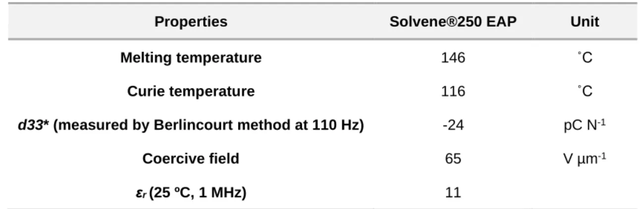
Table 1. Properties of Solvene®250 EAP from SOLVAY SPECIALTY POLYMERS ITALY S.p.A..
Properties Solvene®250 EAP Unit
Melting temperature 146 ˚C
Curie temperature 116 ˚C
d33* (measured by Berlincourt method at 110 Hz) -24 pC N-1
Coercive field 65 V µm-1
εr (25 ºC, 1 MHz) 11
*Values obtained poling at 200 V μm-1, 25 μm thick film printed PEDOT:PSS electrodes.
Some electrodes were printed using a conductive PLA Proto-Pasta (CPLA) from Protoplant. This material is provided in filament and is a compound made of Natureworks 4043D Polylactide (PLA) and conductive carbon black. This provides better electrical properties to the filament represented with the resistance to a length of 10 cm filament and 1.75 mm diameter of 1.8 kΩ and a volume resistivity of 3D printed parts through layers (along the Z-axis) of 115 Ω cm-1.
Sample production
To extrude the filament of Solvene® 250 EAP it was used the Xplore MC5 micro compounder. The
extruding has been done at 150 ˚C, with a nozzle of 1.3 mm and feeding the extruder about 4.5 g of pellets of P(VDF-TrFE) to obtain fibres with 1.75 mm of diameter and length of 1 m.
The extruder has two working modes: speed mode and force mode. The speed mode has been used during the feeding of material and is controlled by the rotating speed of the screws, using a speed of 100 rpm and a maximum force of 3 kN. During the extruding of the fibre, was used the force mode to increase the uniformity of the fibre diameter, using a maximum speed of 300 rpm and a force between 1.4 kN and 1.7 kN, varying to obtain a speed around 28 rpm which also increase the uniformity throughout the fibre.
Study of P(VDF-TrFE) for Structures via 3D Printing
10
The extruder only can be fed with a maximum of 5 g each time, which limits the length of the filament to a maximum around 1 meter. To feed the 3D printer it is required a long filament, so it has been used a piece of brass with a groove with a diameter of 1.75 mm which has been heated around 170 ˚C to merge the extruder fibres to each other.
In the design of the P(VDF-TrFE) film it was used Autodesk Fusion 360, drawing a film with a square shape with 15 mm side and 0.03 mm of height. After the design of the films it was used Ultimaker Cura 4.0.0 to choose the specific parameters of the 3D printing for Creality Ender-3. Some of these parameters were the print speed, layer height, infill density and even the thickness of the wall that is very important in the quality of films with just a few layers of material. In section C of appendices there is more information about the parameters used in the printing of P(VDF-TrFE) films.
The production of samples in 3D printer ends with the printing of the design pieces in Creality Ender-3, using a bed printer of glass at 60 ˚C and a nozzle of 0.4 mm at 200 ˚C. Before the printing, the printer has been calibrated and it was used a hair spray in bed printer to enhance the adhesion of the first layer to the stage.
Only one layer is printed during the printing of P(VDF-TrFE) films to obtain the minimum thickness of this film. To enhance the quality of the surface was used a feature of 3D printer called ironing. This process consists in a second layer where the nozzle does not extrude any material but stay at 200 ˚C and smooth the surface when passing over the printing layer.
The sheet resistance of CPLA was studied to understand how it could obtain electrodes with the best electrical properties. To study the sheet resistance of conductive PLA Proto-Pasta it was designed and printed samples using the same process used in P(VDF-TrFE) films but with 15 mm × 20 mm and up to five layers, each layer with 0.03 mm of height and without using the ironing feature. In a second step, the samples were covered at the ends along the longer axis with water-based silver conductive ink (PE-WB-1078) from Conductive Compounds to create electrodes. Half of the samples were dried at room temperature and the other was dried 3 min at 155 ˚C on a hotplate. This difference in the drying process was performed to study if there is a significant influence on the conductivity of the material related to different temperatures. Lastly, it was measured the resistance between electrodes made of silver conductive ink with a multimeter and it was calculated the sheet resistance for samples with a different number of layers and with variations on the drying process.
The design of electrodes was also done in Autodesk Fusion 360 where electrodes were defined as circles with 10 mm of diameter and 0.12 mm of height using conductive PLA Proto-Pasta. To choose the printing parameters it was used the same way of films but using a smaller wall thickness which is related to the shape of the electrode. In these electrodes it was not used ironing because the difference was not significant and does not compensate the increase of printing time. In section C of appendices is more information about the parameters used in the printing of CPLA electrodes.
11
To obtain electrodes it was deposited aluminium (Al) in P(VDF-TrFE) film by evaporation using masks of circles with 10 mm of diameter. The deposition of 85 nm of Al was made on both sides of the film in order to prepare the sample to the step of polarization, with a current around 55 A and a deposition rate around 0.5 nm s-1.
Sample characterization
During the production of the samples, the materials were tested in different states, since from the pellets of Solvene® 250 until the films and conductive PLA Proto-Pasta. To understand if there are
differences in the physical properties of the material it was made Differential Scanning Calorimetry (DSC) with the Simultaneous Thermal Analyser STA 449 F3 Jupiter to pellets, fibre and films of P(VDF-TrFE) from 20 ˚C to 270 ˚C with a step of 10 ˚C/min.
The same samples were also structurally characterized with X-Ray Diffraction (XRD) using the PANalytical X’pert PRO MRD with a monochromatic Cu-Kα (wavelength 1.5406 Å) radiation source, applying 40 mA of current and 45 kV of voltage, with a 2θ range between 10˚ and 60˚. To obtain a better characterization of the possible changes in the different stages of the material it was done an analysis on Fourier-Transform Infrared Spectroscopy (FTIR) using Thermo Nicolet 6700 with a wavelength between 525 cm-1 and 4500 cm-1 with a 4 cm-1 resolution.
To verify the composition of the conductive PLA Proto-Pasta it was made a chemical analysis to a printed round electrode with Scanning Electron Microscopy (SEM) Hitachi TM3030Plus tabletop workstation using Energy Dispersive Spectroscopy (EDS).
Finally, it was used the Optical Microscope Olympus BX51 to see the morphology of all samples (P(VDF-TrFE) film, the round electrode of CPLA and the samples used to study the sheet resistance) to compare the top and bottom surfaces of each sample. In the case of samples used for the study of sheet resistance it was theorized if it could be helpful to understand the differences in electrical properties between them.
Electrical characterization
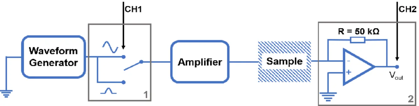
The electrical characterization started with the samples polarisation using a setup composed by a 100 MHz TGA12104 arbitrary waveform generator from Aim-TTi, a TREK MODEL 610E amplifier, a TDS 2001C oscilloscope from Tektronix and equipment to rectify the signal. The signal rectification was done in zone 1 of Figure 3, based on the electric circuit presented in section D of appendices. It was also used a circuit based on the scheme displayed in section E of appendices which could be simplified with an Op Amps TL082 with a 50 kΩ resistance, shown in zone 2 of Figure 3.
Study of P(VDF-TrFE) for Structures via 3D Printing
12 Figure 3. Used setup in samples polarisation.
The applied electric field was increased until evidence of polarization was observed. The amplifier can amplify 100 or 1000 times the signal that came from the waveform generator, which previously passes for the rectify equipment to define what signal will achieve the sample.
After seeing an evidence of polarisation, the sinusoidal signal is rectified to a half signal. The rectification it was done to retain the polarisation in the sample. To align the dipoles in one orientation is primordial the use of unipolar signal because by using a bipolar sinusoidal signal the dipoles will always change their orientation. Finally, the oscilloscope usage is measured by the generated signal before the amplification and the output voltage (Vout), which is important to calculate the current which
passes the sample. Beyond the Vout is crucial known the value of the resistance in zone 2, because
without that value is not possible to obtain the current by Ohm’s Law.
The polarisation is easily achieved using mid temperatures because the material is softened and the dipoles gain larger mobility which enables the alignment of dipoles with lower electric fields. The best way to obtain a homogenous temperature of the sample during the polling process is by using a silicone bath at 90 ˚C, heated with a hotplate. In section F of appendices is presented a sample during the polarisation.
In order to characterize the samples after polarisation it is used a setup with a TGA12104 arbitrary waveform generator 100 MHz from Aim-TTi, a power supply, a 617 programmable electrometer from Keithley Instruments, a temperature sensor, a peltier and an Arduino controller, shown in Figure 4.
13
The working principle of the previous setup is based on the variation of the temperature and measurements of currents and voltages that are generated by the electroactive film at the same time. The waveform generator is used to control the variation of the temperature using the offset parameter to set the average temperature and the applied voltage to define how much the temperature varies around the temperature set by offset. In these measurements is used an offset of 1.8 V, a voltage peak-to-peak of 2.5 V and a frequency of 0.1 Hz. The variation of the temperature of peltier is controlled by the power supply which is consequently controlled by the controller. At the same time, this variation is measured by a temperature sensor which is connected to the controller which sends that information to the computer (PC). While the peltier is working, the sample is heated and generates a current or voltage which is measured by the electrometer that sends the values to the PC using a GPIB connection. In the computer is used a script in Matlab that plots the received values of temperature and current or voltage versus time. In Figure 25 of section G of appendices is presented a sample during the measurements of pyroelectric responses.
The measurement of the capacitance of the samples is performed by inserting films between two plates, as shown in section H of appendices, which are connected to the 4294A Precision Impedance Analyzer from Agilent to obtain the results.
Device production and experiments
The device is designed in Autodesk Fusion 360, shown in section I of appendices, and printed in the 3D printer used for the production of the films. It was projected to put the sample between the two pieces which have printed conductive tracks using CPLA and using commercial PLA to give structural basis to this full printable pyroelectric sensor.
This device is done to prove that the produced and polarised films have good properties to use them in a sensor. It was measured the signal when the sample is submitted to the radiation of a simple halogen lamp to confirm the capabilities of the produced structures, using the simple setup presented in section J of appendices.
15
Results and Discussion
This chapter begins with an electrical and morphological characterization of the printed electrodes and is also performed a study about the sheet resistance of them. The next step in this work is a discussion on P(VDF-TrFE) films, studying the influence of processes during the production of the films, since pellets shape to film, to obtain the maximum information about the material. The work ends with the characterization of the films in order to obtain information about the influence of the applied electric fields and used electrodes in the polarisation. The ferroelectric properties of the material were also studied to understand the possibility of implementing it on a pyroelectric device.
Conductive PLA characterization
The characterization of conductive PLA begins with studying the influence of the number of layers in the sheet resistance (Rsh) of the CPLA. There were used 20 samples in this study, changing the
number of layers between 1 and 5 (in batches of 4 samples each one). Silver conductive ink was used to create the electrodes in the samples. Half of the samples were dried at room temperature (RT) and the remaining samples were dried 3 min at 155 ˚C on a hotplate (HP). This division ensured that two samples submitted with the exact same parameters (number of layers and dry process) were used to obtain a better precision in the results. The resistance (R) measured according to equation 4 with a multimeter between the electrodes was used to calculate the sheet resistance using equation 5, where
ρ is the resistivity, t is the thickness of the sample, L the distance between electrodes and W the
perpendicular distance to L.[60] R = ρ∙ L W∙t = ρ t∙ L W (4)
The ratio between resistivity and thickness is named sheet resistance, which results in the Ω/□ unit.[60]
Rsh = R∙W
L (5)
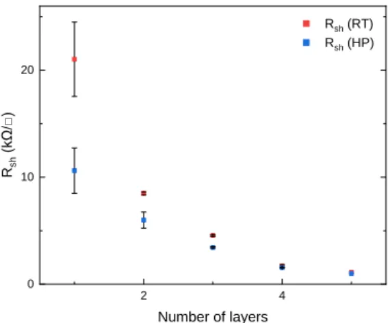
The relationship between the number of layers and the obtained sheet resistance was exposed in Figure 5.
Figure 5. Study of sheet resistance with the increasing of the number of layers and comparison between the room temperature dry process of silver conductive ink electrodes with dry of 3 min in hotplate at 155 ˚C.
2 4 0 10 20 Rsh (RT) Rsh (HP) Rsh (kΩ/□) Number of layers
Study of P(VDF-TrFE) for Structures via 3D Printing
16
With the analysis of Figure 5 it has been clearly seen a decrease in the sheet resistance with the increasing number of layers. This was expected due to the inverse proportionally between the sheet resistance and thickness. In Table 2 is presented the values of the sheet resistance of each sample with different number of layers, for samples dried at room temperature and on a hotplate.
Table 2. Resume of sheet resistance characterization.
Number of layers Rsh (RT samples) Rsh (HP samples)
1 21.03 ± 3.48 10.62 ± 2.12
2 8.50 ± 0.13 6.00 ± 0.75
3 4.56 ± 0.06 3.44 ± 0.06
4 1.72 ± 0.11 1.56 ± 0.02
5 1.13 ± 0 1 ± 0
Beyond the inverse proportionality, the Rsh tends to stabilize at 1 kΩ/□ in both dry processes.
Comparing the samples with the same number of layers but submitted to different dry processes is easily observed that samples dried in a hotplate have lower sheet resistances than samples dried at room temperature. This difference could be related to a promoted annealing of the samples during the drying process which will turn the surface into a more homogenous one.
It is also denoted a decrease in the stiffness of the samples with the increasing of the number of layers and a difference between the first printed layer (bottom surface) and the last printed layer (top layer).
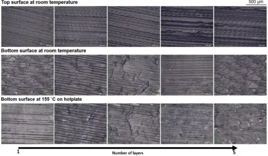
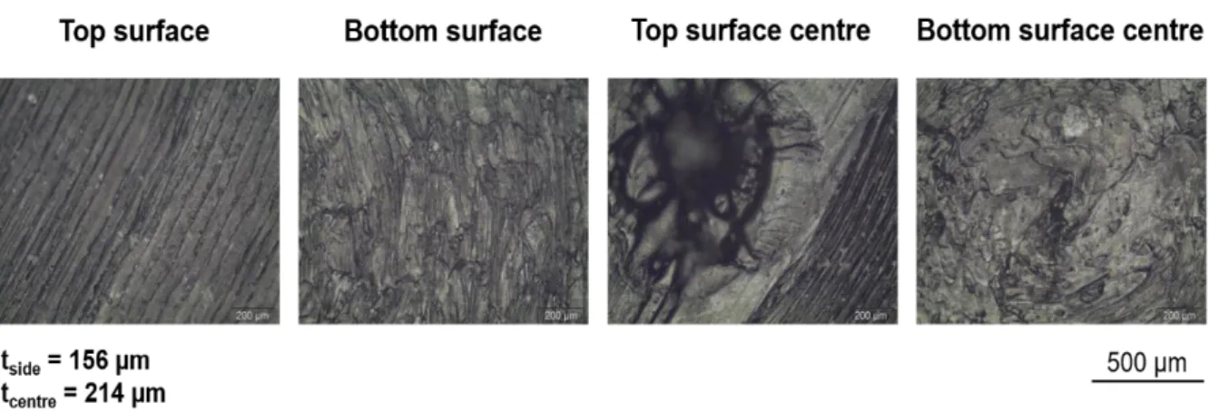
Sample surfaces with a different number of layers were observed using an optical microscope, in order to study the annealing influence of the samples as well their morphological characteristics. The top and bottom surfaces of samples at room temperature and the bottom surface of samples dried on a hotplate were compared in Figure 6. To see the images of the top surface of samples dried on hotplate go to section K of appendices.
Figure 6. Morphological images of the top and bottom surfaces of used sheet resistance samples, with a different number of layers and different dry processes.
17
The analysis of the morphology of the samples was done in two parts: comparison between the top and bottom surface of the same sample and between the same surface of different samples. Beginning with an analysis of the same sample is observed that the bottom surfaces (BS) have a more homogenous surface comparing with the top surface (TS). When analysing the influence of the different number of layers have in the surfaces is easily observed that there is an increase of irregularities on the top surface with the increase of layers. This is justified by the lower resolution of printing process, where the irregularities are propagated layer by layer due to the new layers being printed over layers that are already irregular.
The influence of increasing the number of printing layers is visible in the BS with the increasing of cracks and flaws, which is an explanation of the decreasing of the stiffness observed previously. The origin of these defects is related to the degradation of the material caused by the longer exposure of printing layers to the nozzle at higher temperatures during the printing of new layers. It was observed more defects on the samples with more layers.
The morphological analysis ends with the comparison between the surface of samples dried at room temperature and on a hotplate. It was only compared the bottom surfaces because they are the surfaces that show more significant differences. These differences are more visible in bottom surfaces due to the samples being placed with the bottom part in contact with a hotplate and with reduced time of exposure the sample could not heat homogeneously. The HP samples show fewer and smaller defects comparing with RT samples with the same number of layers. These can be justified by the softening of the samples which lead to homogeneity of the surface resulting in lower sheet resistance of heated samples.
It was concluded that the best option is producing a 3D printed electrode with 4 layers by comparing the obtained results of sheet resistance and morphological analysis. This use case achieved one of the best sheet resistances and at the same time a considerable mechanical resistance due to the absence of critical cracks in the surfaces. The electrodes were not heated for posterior steps, because with this number of layers the difference in sheet resistance is not significant, which could reduce the complexity of the process eliminating this step.
It was performed a morphological analysis to printed electrodes, as shown in Figure 7, expecting similar characteristics to the samples used to calculate the sheet resistance.
Figure 7. Morphological characterization of the 3D printed electrode.
Study of P(VDF-TrFE) for Structures via 3D Printing
18
surfaces in the side of this sample as well the previous samples have a similar irregularity. However, in this sample it was also seen a changing in the thickness between the sides and the centre of the sample. This was caused by the 3D printing process at the end of the printing process which left a small peak of material in this location. This variation in the thickness is not significant in the working of this sample, making unnecessary the use of ironing in this samples in order to spare time in all printing process.
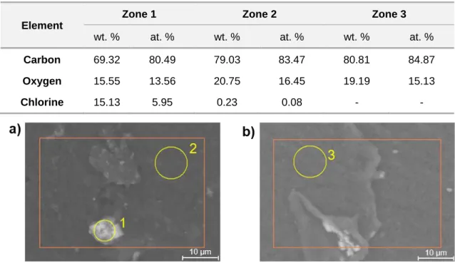
To confirm the composition of the used material it is performed an SEM-EDS analysis presented in Table 3 and Figure 8.
Table 3. Element quantification of 3D printed electrodes by SEM-EDS.
Figure 8. SEM-EDS of 3D printed electrodes of a) top surface, and b) bottom surface.
Analysing simultaneously the previous table and figure it is easily concluded that the material corresponds to the expected conductive PLA, composed by PLA and carbon black. This is possible to conclude by the huge quantity of carbon in both analysed zones and surfaces. In the zones 1 and 2 there is present chlorine, especially in the zone 1 which have high quantity in a particle that is considered a contamination which can be related to the use of hair spray in the printing process of the samples. At the same time it is not found significant quantities of chlorine and the shape is singular and not shows repeatability, as can be observed in Figure 8 (a).
P(VDF-TrFE) characterization
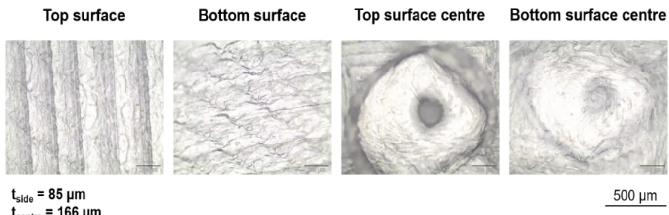
In this work, there were produced three types of P(VDF-TrFE) films with the main objective of understanding which is the best option to polarize and turn the production an easier and faster process. The first produced film is a one layer film (OLF) which has a top surface too much irregular for the required application and has a huge difference between the thickness over the sample. This variation in the thickness, shown in Figure 9, is not great to obtain a uniform polarisation of the sample. That can be a problem in the process because of the requirement to use higher electric fields in some thicker
Element
Zone 1 Zone 2 Zone 3
wt. % at. % wt. % at. % wt. % at. %
Carbon 69.32 80.49 79.03 83.47 80.81 84.87
Oxygen 15.55 13.56 20.75 16.45 19.19 15.13
19
zones with 166 µm which causes disruption of the sample in the thinner zones with 85 µm.
Figure 9. Morphological characterization of one layer printed film without ironing (OLF).
It was found a way to transform this same sample in one of uniform thickness and also decrease the irregularities in the surfaces in order to solve this problem of poor uniformity of the thickness along the sample surface. This was resolved by pressing two of the previous samples with both top surfaces against each other. The pressing process was done 3 min at 140 ˚C to soften the material and increase the adhesion of both films. Figure 10 shows the morphology of the surface of these two layers pressed film (TLPF), showing a more homogenous surface and without significant variations in sample thickness.
Figure 10. Morphological characterization of two layers pressed film.
It is noticed however the presence of small bubbles in the films what is a disadvantage against OLF. These defects can cause a disruption of the sample during the polarisation explained in the work of Navid et al.[61] with the variation in values of resistivity between commercial films with a similar composition of the used in this work, pure films and porous films. This relationship between samples resistivity shows a lower resistivity of a porous film against a commercial one which is related to the presence of pores that will result in a non-uniform electric field in the sample. Another disadvantage of this film is the large thickness of about 100 µm, meaning that it is required a higher electric field to polarise the sample.
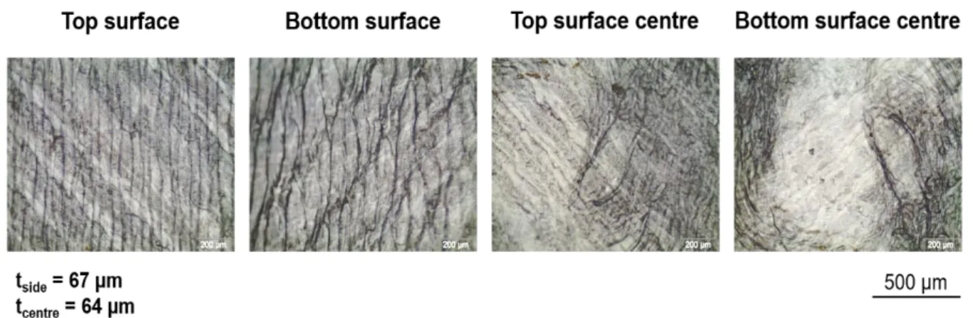
The last type of studied films could be a solution to obtain a film with homogeneous surface and without bubbles which may be a problem in the polling process. These films are one layer materials as the OLF but with an ironing treatment, which will smooth the top surface that normally shows more irregularities. The one layer printed film with ironing (OLFI) have the morphology shown in Figure 11, and is a thinner film about 65 µm with a similar appearance of the top and bottom surfaces, even in the
Study of P(VDF-TrFE) for Structures via 3D Printing
20 centre what not occur in OLF.
Figure 11. Morphological characterization of one layer printed film with ironing (OLFI).
Looking into the morphological images of three types of produced films and thinking about the complexity of the fabric process of each sample some conclusions can be obtained about which film has the best properties.
The OLF has just the reduced time as an advantage due to the complexity of the process being similar to OLFI and the top surfaces of these films are too much irregular and with a large variety of thickness over the sample. On the other hand, the TLPF has just great homogeneity of surfaces as its main characteristic of the required application for the film. When compared to other films, the TLPF have drawbacks like the need for an extra process to press the films after the 3D printing process. It also has limited to larger thicknesses, due to being a result of pressing two layers of OLF. Lastly, it also has the limitation of the bubbles which can cause a disruption of the material too earlier.
The last presented type of produced films only has one disadvantage that is a longer duration of the 3D printing process. Nevertheless, the increasing time is not relevant in the total printing time of OLFI. On the other hand, these films are made in just one process and with just one equipment, having nice similarities and a uniform displacement in both surfaces, with no significant irregularities. They are the thinnest films when compared with the remaining options. Regarding the analysis of morphology, the OLF is considered a not so good option, which lead to its exclusion in the next characterizations.
The DSC experiment, shown in Figure 12, was made to verify if exists any significant differences in the peak of Curie temperature and fusion temperature in pellet, fibre, TLPF and OLFI. The peaks around 116 ˚C represent the Curie temperature while the fusion temperature is represented in the peaks around 140 ˚C. Analysing the results, it is possible to conclude that it does not exist significant differences between the positions of the peaks, which means that during the process the material does not change its properties.
21
Figure 12. DSC spectra of P(VDF-TrFE) pellet, fibre, TLPF and OLFI.
To study the crystalline phase of the different stages of P(VDF-TrFE) during the work there were characterized pellets, fibres, TLPF and OLFI via FTIR, shown in Figure 13. The TLPF still needs to be studied in order to understand if it could be a viable option to produce an electroactive device, although showing that the morphology could be a problem in its polarisation.
Figure 13. FTIR spectra of P(VDF-TrFE) pellet, fibre, TLPF and OLFI.
Analysing the FTIR spectra it is observed a presence of three characteristic absorption peaks of β phase at 839, 1284 and 1398 cm-1 which are related with the P(VDF-TrFE) dipoles orientation. The peak
at 1398 cm-1 is assigned to CH2 wagging vibration and symmetric stretching. The peaks with a
wavenumber of 839 and 1284 cm-1 are assigned to symmetric stretching of CF2 and CH2, respectively.
These three characteristic peaks are also related to symmetric stretching of CC. Beyond these characteristic peaks there are two visible intense peaks at 878 and 1164 cm-1 related with rocking and
asymmetric stretching of CF2 and rocking of CH2 only at 878 cm-1. [62], [63]
Comparing the four spectra it is observed a big difference between pellets and the other three, which is related to the fact of pellets do not being submitted to processes with a temperature near to melting
100 125 150 -0.6 -0.4 -0.2 0.0 0.2 0.4 DSC (m W mg -1) Temperature (ºC) Pellet Fibre TLPF OLFI exo 1400 1200 1000 800 0.0 0.2 0.4 0.6 0.8 839 cm-1 Absor ba nce (a .u. ) Wavenumber (cm-1) Pellet Fibre TLPF OLFI 1398 cm-1 1284 cm-1
Study of P(VDF-TrFE) for Structures via 3D Printing
22
point. This will influence the intensity of the peaks due to the tendency of the copolymer to crystallize in β phase after solidification. When the pellet is transformed in fibre it suffers a melting process which increases the presence of β phase. Using the same logic is observed a small difference between fibre and OLFI because the second one is submitted to a melting process during the printing process. Nevertheless, the melting and solidifying process of the material is too fast and it does not have a big influence in the phases of the material. As TLPF is submitted to a pressing process using a temperature near to melting point for some time it occurs crystallization in β phase in the solidification.[42], [46]
XRD was done with the main objective of verifying if exists any structural differences between pellet, fibre, TLPF and OLFI. The result of this analysis is shown in Figure 14.
Figure 14. XRD spectra of P(VDF-TrFE) pellet, fibre, TLPF and OLFI.
Accordingly with Oliveira et al.[46] is detected three characteristics peaks of β phase of P(VDF-TrFE) in all samples at 19.85˚, 35.24˚ and 40.75˚. The increase of peaks intensity of pellet to TLPF is explained with the use of temperature near to Tc and melting point of the material that was previously
explained in FTIR analysis.
The lower intensity curve of fibre when compared with films could be explained with the loss of crystalline structure during the melting process which allows to molecules and atoms to move randomly.[63], [64] Although the films were submitted to temperature, other parameters which influence the crystallinity are the duration of the melting process and the rate of heating and cooling.[46] These parameters explain the higher intensity of peaks of films comparing with fibre because in the production of the second one the material still melting for more time.
The OLFI uses a higher temperature than in fibre production which could influence the decrease of the peak intensity but analysing the XRD curve this does not happen. The peak of OLFI is higher than fibre because of the quantity of material that is fed by the 3D printer during the printing is much less than in fibre production. This decreases the cooling time and transforms almost entirely α phase presented in molten material into β phase.[46], [64]
20 30 40 50 0 10000 20000 30000 40000 Int en sity (a .u. ) 2q (º) Pellet Fibre OLFI TLPF (110)b & (200)b 2q = 19.85º (201)b 2q = 40.75º (001)b 2q = 35.24º
![Figure 1. Schematic diagram of the FDM process based on [4].](https://thumb-eu.123doks.com/thumbv2/123dok_br/15792989.1078373/25.892.323.580.689.942/figure-schematic-diagram-fdm-process-based.webp)
![Figure 2. Ferroelectric a) phase transition of ferroelectric to paraelectric b) polarization hysteresis from [30]](https://thumb-eu.123doks.com/thumbv2/123dok_br/15792989.1078373/28.892.218.666.354.498/figure-ferroelectric-phase-transition-ferroelectric-paraelectric-polarization-hysteresis.webp)