Homogeneous Gaussian Profile P
+-Type Emitters:
Updated Parameters and Metal-Grid Optimization
M. Cid, N. Stem*
Laboratório de Microeletrônica – Depto. de Engenharia de Sistemas Eletrônicos Escola Politécnica da Universidade de São Paulo
C.P. 61548, 05424-970 São Paulo - SP, Brazil
Received: May 4, 2001; Revised: April 16, 2002
P+-type emitters were optimized keeping the base parameters constant. Updated internal
pa-rameters were considered. The surface recombination velocity was considered variable with the surface doping level. Passivated homogeneous emitters were found to have low emitter recombi-nation density and high collection efficiency. A complete structure p+nn+ was analyzed, taking into
account optimized shadowing and metal-contacted factors for laboratory cells as function of the surface doping level and the emitter thickness. The base parameters were kept constant to make
the emitter characteristics evident. The most efficient P+-type passivated homogeneous emitters,
provide efficiencies around 21% for a wide range of emitter sheet resistivity (50 – 500 Ω/) with
the surface doping levels Ns= 1 × 1019 cm-3 and 5 × 1019 cm-3. The output electrical parameters
were evaluated considering the recently proposed value ni= 9.65 × 10
9 (cm-3). A non-significant
increase of 0.1% in the efficiency was obtained, validating all the conclusions obtained in this
work, considering ni= 1 × 10
10 cm-3.
Keywords: theoretical optimization, homogeneous passivated emitters, p+-type, Gaussian
pro-file, metal-grid
1. Introduction
It is well-known that some effects such as band gap nar-rowing, Fermi level degeneracy and changes on behavior of minority carrier lifetime and mobility occur when a re-gion is highly doped, as for solar cell emitters. Many theo-retical optimizations have been made taking these effects
into account1,2. According to these theoretical predictions
the best p+-type passivated homogeneous emitters were
found to have surface doping level Ns= 1 × 1019 cm-3 and
thickness We = 4 µm, for conventional cells with finger width of 100 µm.
Traditionally, the passivated emitter surface
recombina-tion velocity has been considered constant Sp= 1640 cm/s.
Recently, A. Cuevas et al.3 showed the dependence of the
surface recombination velocity on the surface doping level, making new optimizations imperative.
In this work, theoretical models with analytical
solu-tions have been used to study p+ emitter regions. The
re-combination and collection efficiency are written as func-tion of series of multiple integrals and in order to assure good accuracy, a fifth order approximation was considered.
A simulator code was developed to optimize each particu-lar region of the soparticu-lar cell (emitter, base and n+ region) and
the complete structure p+nn+. In this code a Gaussian
pro-file was chosen and the passivated homogeneous emitters were optimized. Emitters had the recombination current density and efficiency collection calculated as function of the surface doping level and sheet resistivity, considering
passivated region surface recombination velocity variable3.
The surface recombination velocity was kept constant for metal contacted region, Sn= 3 × 106 cm/s.
To calculate theoretical solar cell efficiency, a complete
p+nn+ structure was considered. The base region was
as-sumed to have 300 µm thickness and resistivity of 2.3 Ω.cm.
The lifetime was assumed to be 1.5 ms4. In order to make
the emitter influence evident, the rear surface recombina-tion velocity and the base recombinarecombina-tion current density were assumed to be null. Neither light trapping effects and nor surface reflection have been taken into account. The short-circuit current density was obtained adopting the stand-ard spectrum AM1.5G (ASTM892-87) and updated optical absorption coefficients5.
The metal-grid optimization was carried out using the
traditional expressions to calculate the power loss6 and sidering typical laboratory solar cells with Ti-Pd-Ag
con-tacts with finger width of 5µm and 30µm before and after
electroplating, respectively.
The shadowing factor, Fs, and the metal grid factor, Fm, were optimized as function of the emitter sheet resistivity and the correspondent metal-semiconductor contact resis-tivity. The metal-semiconductor contact resistivity depend-ence on surface doping level was extracted from Swirhun
curves7. An interactive process was adopted and the
opti-mum shadowing factor for each surface doping level was obtained when the normalized total loss power (grid loss power, contact metal-semiconductor loss power and loss power due to the lateral current flow in the emitter) became equal to the shadowing loss, assuring an accuracy of 0.1%. The metal sheet resistivity (Ag) was assumed to be con-stant, ρc≈2 mΩ8. In order to make evident the emitter char-acteristics, the base loss power was assumed to be null.
Thus, the optimum metal-contacted factor, Fm, was
cal-culated taking into account the optimum shadowing factor,
Fs, for each surface doping level according to Eq. 1.
Fm = (17%) x Fs (1)
The output parameters (short-circuit current density, Jsc, open-circuit voltage, Voc and efficiency, η) and the intrinsic
fill factor, FFO were calculated using well-known
relation-ships6. The final fill factor, FF presented in Eq. 2 takes into
account the optimum normalized grid loss power, Pt and
the intrinsic fill factor, FFO.
o FF ) t P (1
FF= − × (2)
2. Updated Internal Parameters and
Expres-sions
Table 1 shows the expressions and the internal param-eters that were adopted in this work. It can be observed that
the intrinsic concentration was assumed to be 1×1010 cm-3
and an updated surface recombination velocity was consid-ered dependent on surface doping level for passivated re-gion3.
All the calculations in this work were made adopting
ni= 1 × 1010 cm-3, despite the recent change9 to
ni= 9.65 × 109cm-3 9, since the former is still the most ac-cepted in the scientific community.
Although initially developed for the outdated value of ni= 1.45 × 1010 cm-3, the minority carrier mobility and band
gap narrowing expressions2 presented in Table 1 keep on
being the best fitting to the experimental results. These empirical expressions were obtained with the PCD tech-nique, by the measurement of the reason Jo/ni2. Therefore, a change of ni only interferes in the obtained Jo and not in the
reason Jo/ni2. Thus, the minority carrier mobility and the
band gap narrowing expressions are independent on ni. This
conclusion is quite important, because it validates the
ex-pressions presented in Table 1 for both ni= 1 × 1010 cm-3
and the recently proposed ni= 9.65 × 109 cm-3 (for 300 K).
3. Emitter Optimization
3.1. Recombination
Figure 1 shows current densities for two kinds of re-gions (metal-contacted and passivated) as function of emit-ter sheet resistivity, R and doping level, Ns, considering their respective surface recombination velocities, Sp= 3 × 106 cm/s and S
p= 500 (Na/10
16)1/3 cm/s.
It can be observed that for metal-contacted regions the recombination current density decreases as the surface dop-ing level and the emitter sheet resistivity increase (corre-sponding to shallower emitters). Therefore, the best recom-bination current densities are found for thick and highly doped emitters.
However, for the passivated region the lowest recombi-nation current densities were found for low surface doping levels (Ns= 5 × 1018 cm-3 and 1 × 1019 cm-3), being practi-cally constant as emitter sheet resistivity increases. It can be observed that highly doped emitters present lower re-combination than passivated emitters when a low emitter sheet resistivity is considered.
Thus, in order to evaluate the contributions of the metal-contacted and passivated regions to the total recombination (Joe), the surface doping level Ns= 1 × 1019 cm-3 was cho-sen, due to lower metal-semiconductor contact resistivity. To calculate the components, it was taken into account the occupation area of both kinds of regions, metal-contacted and passivated, multiplying the components by the weight Table 1. Internal parameters and expressions for p+-type silicon.
factors, Fm and (1-Fm), respectively, as it can be seen in equa-tion (3).
met J m F pass J ) m F (1 oe
J = − × + × (3)
Figure 2 shows the total emitter recombination current density, Joe, and its components, the passivated, Jpass, and
the metal-contacted, Jmet, region recombination current
den-sities versus emitter thickness, We, considering
Ns= 1 × 1019 cm-3.
In this figure, it can be observed that the passivated com-ponent presents a larger contributition than the metal-con-tacted one, due the difference found in the weight factors of both in Eq. 3.
To make a more detailed evaluation of the total recom-bination current density behavior, each emitter region
re-combination current density (metal-contacted, Jmet, and
passivated, Jpass) was divided into two components: volume
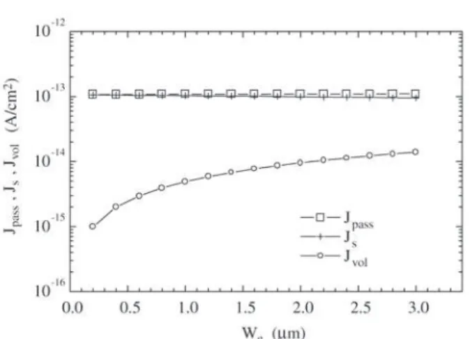
recombination, Jvol and surface recombination, Js, as it can be seen in Figs. 3 and 4.
According to Figs. 3 and 4 the surface recombination current density, Js, is the major contributor to the recombi-nation of both regions (metal-contacted, Jmet, and passivated,
Jpass) about 99.6% and 94.6%, respectively.
However, in Fig. 3, it can be seen in the metal-contacted
region that the volume recombination, Jvol, is practically
constant as the emitter thickness increases, while if it is
compared to Fig. 4, for passivated region, a more signifi-cant contribution of this component is found. In the latter figure the volume recombination increases the contribution about 10 times as the emitter thickness increases from 0.2 to 3.4 µm.
3.2. Emitter collection efficiency
Figure 5 shows a comparison between the emitter col-lection efficiency as function of emitter sheet resistivity and surface doping level, considering homogeneous passivated emitters.
According to this figure, the highly doped emitter col-Figure 1. The total emitter recombination current density, Joe as
function of emitter sheet resistivity, R and surface doping level, Ns, considering two different regions metal-contacted (Sp = 3×106 cm/s) and passivated regions (Sp = 500 (Na/1016)1/ 3 cm/s). Metal-contacted region: - - Ns = 5×10¹⁸ (cm-3), - - N
s = 1×10 19 (cm-3),
-c- Ns = 5×10¹⁹ (cm-3) and -d- N s = 1×10
20 (cm-3). Passivated
re-gion: -V- Ns = 1x10²⁰ (cm-3), -U- N
s = 5×10
19 (cm-3),
- - Ns = 1×10¹⁹ (cm-3) and - - N s = 5×10
18 (cm-3).
Figure 3. The metal-contacted recombination current density, Jmet
and the components surface and volume recombination density, Js
and Jvol respectively versus emitter thickness, We, considering
Ns=1×1019 cm-3 and taking into account the weight factor F m.
Figure 2. The total emitter recombination current density, Joe and the components passivated and metal contacted region recombi-nation current densities, Jpass and Jmet respectively, as function of emitter thickness, considering the surface doping level
Ns=1×1019 cm-3 and taking into account the correspodent weight
lection effciencies are higher than the moderately doped ones since the same value of emitter sheet resistivity is con-sidered. However, when optimized emitters are focused, the moderately doped emitters present slightly higher efficiencies. Thus, analyzing the optimum short-circuit cur-rent densities in Fig. 6 for each surface doping level case, it can be found that the moderately doped emitters present the highest optimum emitter sheet resitivities (the thickest optimized emitters). For instance, chosing the optimum sheet resistivies from Fig. 6 curves, it can be seen in Fig. 5 that the optimized collection efficencies for Ns=5×1018 cm-3 and
Ns=1x1020 cm-3 cases are quite close η
c = (98.4 – 97.9)%
with their correspondent sheet resistivities (255-106) Ω/. One point to be stressed is that such close values are not found when the respective short-circuit current densities are calculated as it can be seen in Fig. 6. In these curves, the maximum short-circuit current densities are quite different when compared moderately and highly doped emitters, Ns = 5×1018 cm-3 and N
s = 1×10
20 cm-3, respectively. This
dif-ference is attributed to the metal-grid shadowing factor (1-Fs) influence.
4. A Complete Structure: P
+NN
+Solar Cells
In order to compare the emitter effects on the complete structure P+nn+, the base and n+ regions have been consid-ered constant. The recombination current density of base Figure 7. Open circuit voltage, Voc as function of emitter sheet resistivity, R and surface doping level, Ns, considering p-type emit-ter solar cells.
Figure 6. Short-circuit current density, Jsc as function of emitter sheet resistivity, R and surface doping level, Ns, considering p-type emitter solar cells.
Figure 5. Emitter collection efficiency, ηc as function of emitter
sheet resistivity, R and surface doping level, Ns,considering
passivated surfaces.
region and the rear surface recombination velocity were assumed to be null, as mentioned before. Thus, the outuput electrical parameters (short-circuit current density, Jsc, open circuit voltage, Voc, and efficiency, η) as function of the emitter sheet resistivity and the surface doping level are shown in Figs. 6-8, respectively.
The short circuit densities, Jsc, were obtained taking into account the photogenerated current densities in emitter and
base regions, considering the weight factor (1-Fs)
corre-spondent to the illuminated area.
According to this figure, the highest short-circuit
densi-ties (approximately Jsc≈38.2 mA/cm2) are reached for
Ns= 5 × 1019 cm-3 and N
s= 1 × 10
20 cm-3,, corresponding to
a wide emitter sheet resistivity range R= (185-93) Ω/ and R= (211-71) Ω/ respectively, despite the highest emitter collection efficiency had been obtained for Ns= 5 × 1018 cm-3, as it was shown in Fig. 5. This fact, as
mentioned before, is due to the high shadowing factor, Fs,
provided by the moderately doped emitters, correlated to the increase of the metal-semiconductor contact resistivity. In Fig. 7 it can be observed that the highest open circuit voltage are reached for the sheet resistivity ranges
(10-100) Ω/ and (25-200) Ω/ corresponding to relatively deep, and moderately doped emitters, (Ns= 5 × 1018 cm-3 – 1 × 1019 cm-3), respectively, since they provide the lowest recombination, as it can be seen in Fig. 1.
Thus, as both parameters (short-circuit current density and open-circuit voltage) are competitive, the best surface doping levels are going to be determined by the solar cell efficiencies.
According to Fig. 8, there is a wide range of emitter sheet resistivity (50 – 500 Ω/) that provides efficiencies around 21%, when the surface doping levels Ns= 1 × 1019 cm-3 and 5 × 1019 cm-3 are considered; the most
efficient P+-type passivated homogeneous emitters
corre-spond to η= 21.2% with the thickness range (1.6 – 0.4) µm.
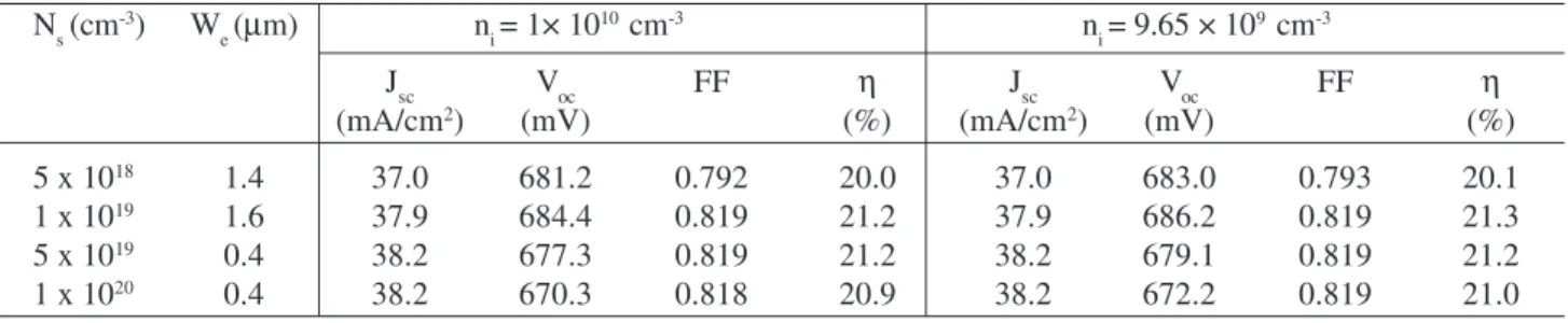
5. Updating Output Electrical Parameters
In order to evaluate the influence of the recently pro-posed ni= 9.65 × 109 cm-3, the optimized output electrical parameters (short-circuit current density, open-circuit volt-age, fill factor and efficiency) were compared for both val-ues of ni, as follows in Table 2.
It can be observed that, if the recently proposed ni is
considered, no modification is obtained in the short-circuit current densities, Jsc, but there is a slight increase in the Voc,
consequently providing a slight increase (≈0.1%) in the
ef-ficiency, η. These results validate the present conclusions
even if small corrections are made in the currently carrier intrinsic concentration ni= 1 × 1010 cm-3 (T = 300 K).
6. Conclusion
Passivated homogeneous p+-type emitters have low
emit-ter recombination (Joe = 1.2 × 10⁻¹³ A/cm2 for
Ns= 1 × 1019 cm-3 and R
=145 Ω/) and are dominated by
the surface recombination component, behaving as
trans-parent emitters for thicknesses up to 3.0 µm.
Gaussian profile p+-type emitters also presented high
emitter collection efficiencies, even if they are highly doped and shallow. It was found that only if the optimized emitter sheet resistivities for each surface doping level is consid-Table 2. Comparison of the electrical output parameters (Jsc, Voc, FF e η), considering ni=1 × 1010 cm-3 and the newest n
i=9.65 × 10 9 cm-3,
for optimized emitters.
Ns(cm-3) W
e (µm) ni= 1× 10
10 cm-3 n
i= 9.65 × 10 9 cm-3
Jsc Voc FF η Jsc Voc FF η
(mA/cm2) (mV) (%) (mA/cm2) (mV) (%)
5 x 10¹⁸ 1.4 37.0 681.2 0.792 20.0 37.0 683.0 0.793 20.1
1 x 10¹⁹ 1.6 37.9 684.4 0.819 21.2 37.9 686.2 0.819 21.3
5 x 10¹⁹ 0.4 38.2 677.3 0.819 21.2 38.2 679.1 0.819 21.2
1 x 10²⁰ 0.4 38.2 670.3 0.818 20.9 38.2 672.2 0.819 21.0
ered, the collection efficiency of the moderated doped emit-ters are slightly higher than the highly doped ones.
As long as the high quality of p+-type homogeneous
emitters was made evident, p+nn+ solar cells optimization
was carried out, taking into account the contribution of the optimum metal-grid and shadowing factors to the output electrical parameters (short-circuit current density, open-circuit voltage and efficiency).
It was found that the metal-semiconductor contact re-sistivity dependence on surface doping level increased the optimum shadowing factor for moderately doped emitters, Ns= 1 × 1019 cm-3 and 5 × 1018 cm-3; and therefore, decreas-ing their short-circuit current densities. On the other hand, the moderately doped emitters also presented the highest open-circuit voltages due to their excellent recombination current densities.
Thus, there is a trade-off between both parameters (short-circuit current density and open-(short-circuit voltage), the
maxi-mum efficiencies, η ≈21.2% were found for the surface
dop-ing levels (1 × 10¹⁹ - 5 × 10¹⁹) cm-3, emitter thicknesses range
(1.6 and 0.4) µm and sheet resistivities (145 – 185) Ω/,
respectively. Another point to stress is that these surface doping levels can provide efficiencies around 21% for a wide range of emitter sheet resistivity (50 – 500 Ω/).
Although in this work all theoretical optimizations were made considering ni = 1 × 1010 cm-3, a brief evaluation of the recently proposed value influence (ni= 9.65 × 109 cm-3) on the optimized results showed a non-significant change, validating all present conclusions.
Aknowledgments
This work was supported by FAPESP under contract
no95/09435-0.
References
1. Cuevas, A.; Merchán, R.; Ramos, J.C. “Updated contour
plots for the design of p+ emitters of silicon solar cells”,
In Proceedings of the 23rd IEEE Photovoltaic Specialists
Conference, IEEE Press, New York, p. 309-314, Confer-ence held in Lousville, K.Y., USA, 1993.
2. King, R.R. “Studies of diffused boron emitters:
satura-tion current, bandgap narrowing, and surface recombi-nation velocity”, IEEE Transactions on Electron Devices, v. 38, n. 6, p.1399 – 1409, June 1991.
3. Cuevas, A.; Stuckings, M.; Lau, J.; Petravic, M. “The
recombination velocity of boron diffused silicon sur-faces”, In Proceedings of 14th European Photovoltaic
Solar Energy Conference and Exhibition, Conference held in Barcelona (Catalunya), Spain, 30 June-4 July, 1997.
4. Verliden, P.J.; Sinton, R.A.; Wichkan, K.; Crane, R.A.;
Swanson, R.M. “Backside-contact silicon solar cells with
improved efficiency for the ’96 World Solar Challenge’ ”,
In Proceedings of 14th European Photovoltaic Solar
En-ergy Conference and Exhibition, p. 96-99, Conference held in Barcelona, Spain, 30 June – 4 July, 1997.
5. Green, M.A.; Keevers, M.J. “Optical properties of
in-trinsic silicon at 300K”, Progress in Photovoltaics, v. 3, n. 3, p. 189-192, May 1995.
6. Green, M.A. “Solar cells: optimization principles,
tech-nology and system applications”, p.78, (Englewood Cliffs: Prentice Hall), 1982.
7. Swirhun, S.E., PhD Dissertation, Stanford University, 1987.
8. Cuevas, A.; Russel, D.A. “Co-optimization of the
emit-ter region and metal grid of silicon solar cells”, Progress in Photovoltaics, v. 8, n. 6, p. 603-616, 2000.
9. Altermatt, P.P.; Schumacher, J.O.; Cuevas, A.; Glunz,
S.W.; King, R.R.; Heiser, G.; Schenk, A. “The extraction
of the surface recombination velocity of Si: P emitters using advanced silicon models”, In CD-ROM of 16th