NORMALIZED STATICAL ANALYSIS WITH FREQUENCY AND LOAD
VARIATION FOR THE CLASS-E CONVERTER BASED ON
PIEZOELECTRIC TRANSFORMERS
Raffael Engleitner
∗José Renes Pinheiro
∗Fábio Ecke Bisogno
∗Matthias Radecker
†Yujia Yang
†∗UNIVERSIDADE FEDERAL DE SANTA MARIA – UFSM/PPGEE/GEPOC
Avenida Roraima, no1000, Cidade Universitária.
Santa Maria, RS, Brazil - 97105-900.
†FRAUNHOFER INSTITUT FOR RELIABILITY AND MICROINTEGRATION
Gustav-Meyer-Alee-25, Berlin, Germany - 13355
RESUMO
Análise Estática Normalizada com Variação de Frequên-cia e Carga para o Conversor Classe-E utilizando Trans-formadores Piezoelétricos
Os transformadores Piezoelétricos permitem o projeto de aplicações promissoras para fontes de alimentação até 100W, melhorando a eficiência, reduzindo o tamanho, facilitando a obtenção de grandes relações de transformação, além de proporcionar alta imunidade contra ruídos eletromagnéticos e interferências. Por apresentarem um modelo elétrico equi-valente de característica ressonante, utilizam-se topologias de conversores ressonantes para projetar estes conversores, como por exemplo, a topologia Classe-E. Para facilitar a aná-lise de conversores de ordem superior, pode-se utilizar um método de análise normalizado. O controle do conversor Classe-E utilizando transformadores piezoelétricos é imple-mentado através da variação da freqüência e da razão cíclica de operação. O ganho estático é regulado através da varia-ção da freqüência de chaveamento, e a razão cíclica muda
Artigo submetido em 01/03/2011 (Id.: 01282) Revisado em 23/05/2011, 14/07/2011
Aceito sob recomendação do Editor Associado Prof. Carlos Roberto Minussi
para atender as condições de comutação suave para diferen-tes freqüências. Este artigo apresenta uma análise completa normalizada deste processo, incluindo variação normalizada da frequência e carga, permitindo escolher um ponto ótimo de projeto estático e avaliar seu comportamento com a va-riação de frequência, sem a necessidade de parâmetros de projeto. São mostrados resultados experimentais para um conversor abaixador de 3W, para uma entrada universal de 85-260 V AC e saída de 6 V DC, para validar a metodologia apresentada.
PALAVRAS-CHAVE: Conversor Classe-E, Conversores Res-sonantes, Transformadores Piezoelétricos, Análise Normali-zada.
ABSTRACT
to build these power supplies, i.e. the Class-E converter. In order to make easier the analysis of high order converters, it’s possible to use a normalized analysis method. The control of the Class-E converter using PTs is implemented through the switching frequency and duty cycle variation. The static gain is achieved though the switching frequency variation, while the duty cycle is adjusted with the purpose of achiev-ing soft switchachiev-ing for different frequencies and loads. This paper shows a normalized analysis of this process, including a normalized frequency and load variation, without the need of design parameters. Experimental results for a 3W step-down converter are shown for a universal 85-260 V AC input and output voltage 6 V DC, to validate the proposed method.
KEYWORDS: Class-E Converter, Resonant Converters, Piezoelectric Transformers, Normalized Circuits Analysis.
1
INTRODUCTION
Piezoelectric Transformers (PTs) are an attractive option in order to reduce size, volume and weight in many low power applications (Yamane et al., 1998; Prieto et al., 2001). Build-ing PTs into resonant topologies as Class-E, Half Bridge, Full Bridge, etc, provides high frequency and fast dynamical response designs (Yamane et al., 1998), allowing ZVS (zero voltage switching) without additional devices (Ninomiya et al., 1994). Therefore, PTs have been used in DC-DC con-verters (Yamane et al., 1998), CCFL (Cold-Cathode Fluores-cente Lamps) backlighting inverters (Shoyama et al., 1997), offline power supplies (Diaz et al., 2001) and LED (light-emitting diode) lighting applications (Bisogno et al., 2006).
A normalized method was shown in (Kazimierczuk and Puczko, 1987), which allows the analysis of any converter using normalized graphics. The methodology avoids any pa-rameter of the application, facilitating considerably the anal-ysis and design of high order resonant topologies.
Later, (Bisogno et al., 2004; Yang et al.,2009) extended this idea, comparing the Class-E and Half Bridge piezoelectric converters. Static analyses concerning gain, ZVS conditions and the parameters selection have been presented. It was shown that this method favors the best operation point se-lection for each converter and allows a comparison between the topologies.
A dynamic model for the Class-E converter was presented by (Bisogno et al., 2005; Nittayarumphong et al., 2005). The method divides the converter in a low frequency circuit, re-lated to the output filter, and a high frequency circuit, con-cerning the resonant part. The authors used frequency mod-ulation (FM) in order to adjust the input-to-output gain to compensate input and load variations. However, the normal-ized methodology was not used. This inconvenience brings
back the necessity of design parameters, as output power, in-put and outin-put voltages, etc.
It is believed that analyzing high order power converter using the normalized method favors the optimum design and topologies comparison. So, an extended normalized overview which includes switching frequency and load nor-malized variations would be very useful. This paper has as the main contribution, the achievement of a static model of the converter, with normalized load and frequency variation.
2
NORMALIZED
ANALYSIS
OF
THE
CLASS-E CONVERTER
The purpose of the analysis is to obtain a numerical solu-tion for many operasolu-tion points so that is possible to compare them and obtain the optimum, without the parameters de-sign. Independently of the operations point, it is forced that the converter operates under ZVS conditions.
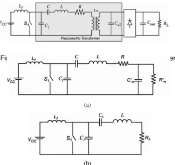
Considering the Class-E topology builded with PTs as shown in Figure 1, the ZVS conditions are obtained when the volt-age at the switch achieves zero naturally before it turns on.
Due to the low-pass filter characteristics of the PT, some sim-plifications can be done in the circuit according to (Bisogno et al., 2004). It is possible to assume the output rectifier plus filter as an equivalent resistance (Req), and after that
contro-vert Cd2and Reqto the primary side of the ideal transformer
of the PT model. Therefore, the circuit becomes simplified as shown in Figure 2a.
The components that are in parallel on the output can be considered as a series arrangement for a fixed switching fre-quency through Equation (1). Further, they can be rearranged with other elements in the circuit according to equation (2). The simplified circuit of Figure 2b is obtained.
RSeq=
Req′
1 +Req′2Ceq′2ω2
and CSeq =
1 +Req′2Ceq′2ω2 Req′2Ceq′ω2
(1)
RS =RSeq+RandCS =
CCSeq C+CSeq
(2)
2.1
Normalization
The first step to normalize the system is based on the differ-ential equations that describe the stages of the circuit. The stages are shown in Figure 3. The equations are obtained according to the circuit of Figure 2b as other authors already proposed (Bisogno et al., 2004; Yang et al., 2009). The wave-forms of the circuit of Figure 2b are shown in Figure 4.
Figure 1: Class-E Converter with Piezoelectric Transformer.
(a)
(b)
Figure 2: Simplified Class-E Converter. (a) Output elements in parallel arrangement. (b) Output elements in series ar-rangement.
(a)
(b)
Figure 3: Stages of the converter at steady state. (a) Stage I - (t0≤ t<t1:DcT). (b) Stage II - (t1≤ t<t2: (1-Dc)T).
Figure 4: : Operation stages at steady state.
Where Dc is the Duty Cycle applied in the switch. The equa-tions obtained have to be represented on state space form, as:
˙
X =AX+BU (3)
As the system is described in two stages, two system will be created, X˙stage1and. The frequency and other
parame-ters from the matrices can be eliminated through constants substitutions. These constants are defined regarding the re-lation between the resonances of the reactive component of the circuit and the switching frequency. Besides, quality fac-tors are defined to eliminate the dissipative elements. These constants are defined as:
ω1= √LCs1 , ω2= √LC1 1, ω3=
1 √LfC
1,
A1=ωω1, A2= ωω2, A3=ωω3andQ1= LωRs1
(4)
Whereωis the switching frequency. Thereby, the following normalized state space system can be achieved:
•
Vc1/Vcc IS1/Icc IL/Icc
.. .
=A(A1,A2,A3,Q1).
Vc1/Vcc IS1/Icc IL/Icc
.. .
+B(A1,A2,A3,Q1).U(t)
(5)
The system is solved for many operation points using math-ematic software. These points contemplate many different values of duty cycle, A1,A2, A3, etc. Normally the input voltage basis is defined first (Vcc), but the input current basis depends on the equivalent DC resistance of the circuit (Rcc). The DC resistance can be defined as a constant (a) multiplied by the output equivalent resistance (Rs), as shown below:
Rcc=aRs, Vcc Icc
=aRs and PoRs
Vcc2
= 1
a (6)
The reverse of this constant, defined as PORS/VCC2, is
called power transfer ratio or quadratic static gain of the con-verter. The power transfer ratio is calculated according to:
1
a =
VO_RM S2 VCC2
= A1
2
2πQ12 2π
Z
0
IL(ωst)2dωst (7)
The details on how to obtain the normalized state space sys-tem and how to derive the power transfer ratio equations are shown in (Bisogno, 2006).
2.2
Normalized Static Analysis
After obtaining the database with the numerical solutions for the Class-E converter for each operation point considering only the nominal frequency. It is possible to evaluate many normalized graphics, for instance, the gain variation for dif-ferent duty cycles, as shown in Figure 5.
good gain in a flat region, with less sensitivity to the duty cycle derivation.
Assuming that A3=1.2 and varying Q1, the gain nearly doesn’t change, as shown in Figure 5b. The variation of Q1 means variation on the load of the converter. The output of the resonant circuit can be considered as a sinusoidal current source, and Q1variations can be neglected when Q1>5.
There are other variables on the system that can be interest-ing for the design, for instance, normalized voltage (VS_pk)
and current (IS_pk) peaks at the switch. The curves can be
observed in Figure 6.
(a)
(b)
Figure 5: Power transfer ratio as function of the Dc,A3 and
Q1.(a) A3Variation. (b) Q1Variation.
(a)
(b)
(c)
Figure 6: Normalized voltage and current peak in the switch as a function of the Dc andQ1. (a) Voltage. (b) Current. (c)
Cp, normalized distribution.
It can be implied from Figure 6 that designing the nominal point for low or high duty cycles, entails on high current or high voltage stresses respectively. It is possible to play with the design point from the right to the left depending on the switch technology and converter input voltage. In other words, it is possible to find a balance between voltage and current peaks. The point Dc=0.5 shows an equilibrium be-tween the extremes. It can be confirmed by the curves in Fig-ure 6c, obtained through the equation (8) for different values of A3:
Cp= 1
Vs_pkIs_pk
(8)
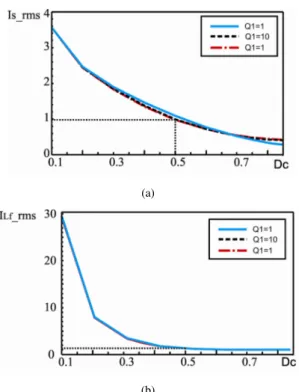
The voltage and current peaks on the switches don’t change significantly for Q1 and A3 variations. The normalized graphic of the rms current in the elements can imply the point where the converter becomes lossier. It is defined IS_rmsand
ILf_rmsas the rms normalized current in the switch and the
input inductor respectively. Both are shown in Figure 7.
(a)
(b)
Figure 7: Rms current in the inductor and in the switch as a function of Dc andQ1. (a) Current in the switch. (b) Current
in the inductor.
It is possible to infer from Figure 7 that the losses are lower for higher duty cycles. Other elements from the circuit be-long to the PT, so the losses are not considered. The effi-ciency of the PT is near the unity (up to 97%) and its losses are not directly proportional to the current, but to physical characteristics related to mechanical oscillation.
3
STATIC MODEL WITH FREQUENCY
VARIATION
When the circuit has to be normalized only for nominal fre-quency analysis, the circuit from Figure 2b returns precise results (Bisogno et al., 2004). However, when the switch-ing frequency changes, the simplification represented by the equation (1) prevents the results to be correct, due toω in the equation. This means that the approximation is valid only for the nominal frequency. To correct that, the differ-ential equations have to be obtained according to the circuit of Figure 2a, not the one from Figure 2b as other authors proposed (Bisogno et al., 2004; Yang et al.,2009). The state space equations are again obtained. The frequency and other parameters from the matrices are again eliminated through constants substitutions. Due to the circuit change, new con-stants are defined in :
ω4=√LC1 ′
eq
, ω5= √LC1 , A4= ωω4,
A5=ωω5,andQ4=LωR′4
eq
(9)
Whereωis the switching frequency. Thereby, the normalized state space system represented by can be achieved:
•
Vc1/Vcc IS1/Icc IL/Icc
.. .
=A(A1,A2,A3,A4,A5,Q1,Q4).
Vc1/Vcc IS1/Icc IL/Icc
.. .
+B(A1,A2,A3,A4,A5,Q1,Q4).U(t)
(10) After the selection of the nominal operation point according to curves as shown in section 2, it is possible to verify how the output can be regulated. As show in (Yang et al., 2004) for different resonant converters topologies, the regulation is achieved through the switching frequency variation close to the resonance of the resonant tank. The maximum gain is achieved at the peak of the resonance. (Yang et al., 2004) also infers that is possible to have ZVS when the converter works on the right side of the resonance curve. The input-to-output regulation can be achieve through the frequency ad-just concerning curves as in Figure 8. These are hypothetical gain curves for the circuit in Figure 1a, considering differ-ent loads represdiffer-ented by Q1.The nominal operation point is given for minimum Q1, where the maximum power transfer is achieved. The load at this point respects the equation (11):
R′eq =
1
ωC′
eq
(11)
Assuming that Q1 minimum is equal 1 as shown in Figure 8, the maximum gain is obtained at the peak of the admit-tance curve (fO1). However, (Diaz et al., 2004) showed that
when ZVS is required, it is necessary to have a distance be-tween the resonance peak and the minimum operation fre-quency. The reason is that some reactive energy is necessary to achieve ZVS. At the peak, current and voltage are totally in phase to each other. Besides, the sensitivity at this point is too high.
Figure 8: Operation regions and resonance frequencies.
This difference is defined as∆f, and implies that the min-imum switching frequency has to be fO1+∆f for nominal
the resonance frequency variation, fO2and fO3. Therefore, it
is assumed that the minimum switching frequency is placed at the point 1 in Figure 8. This point has the maximum gain keeping ZVS, and the frequency can be increased to regulate the converter, for instance the point 2.
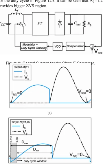
When the load changes to Q1=10 or Q1=100, the ZVS re-gions become 3-4 e 5-4 respectively. Nevertheless, the max-imum gain is defined by the nominal load at point 1, lim-iting the operation between 6-4 for Q1=100, not 5-4 any-more.This statement induces to the conclusion that the min-imum switching frequency takes place at point 1. This is an important conclusion in order to justify the control strategy shown in Figure 9. It is based on the switching frequency and duty cycle variation, always for frequency values higher than the nominal one, at point 1.
To work in this way, the output voltage has to be measured and compared to the reference value. The error is compen-sated and the control voltage goes to a VCO (Voltage Con-trolled Oscillator). The VCO provides the triangular wave which has the switching frequency information.
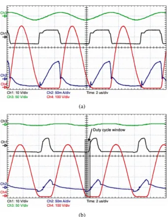
It is important to observe that the normalized analysis method shown in the sections 1 and 2 find always the solu-tion for the point 1 in Figure 8. Thus, the frequency variasolu-tion is not considered. However, if the switching frequency in-creases as a result of the control strategy, the switch turns on while the current goes through the anti-parallel diode, as shown in Figure 10b.
The current (IS1) and the voltage (VS1) in the switch for a
nominal operation point (fS/(fO1+∆f)=1) are shown in
Fig-ure 10a . This point is the point 1 in FigFig-ure 8. FigFig-ure 10b shows the behavior after the frequency being increased. There is a duty cycle window which is shown in Figure 10b. It is defined by the time while the current crosses the anti-parallel diode of the switch. These windows change for each frequency value, but for any point inside this window ZVS can be achieved.
Figure 11 helps to understand the modulator behavior in the control loop from Figure 9. It is suppose to generate a tri-angular wave with variable frequency according to the VCO input voltage, and a duty cycle that respects the ZVS condi-tions. To respect the ZVS conditions, it is necessary to imple-ment a function that adjusts the duty cycle. This function is called duty cycle tracking. So, the main contribution of this paper is the analysis the frequency, load and input variation using the normalized concept, in order to obtain the general duty cycle window of the class-E converter.
So, the main contribution of this paper is the analysis of the frequency, load and input variation using the normalized con-cept, in order to obtain the general duty cycle window of the
class-E converter. With this achievement, it possible to un-derstand the behavior of the circuit for all conditions, and implement the duty cycle traking in the modulator. Figure 12 shows the so called duty cycle window for different Q1and A3. It can be seen that for different loads, with A3constant, the duty cycle window changes considerably in Figure 12a.
For Q1constant, depending on A3, there are different regions for the duty cycle in Figure 12b. It can be seen that A3=1.2 provides bigger ZVS region.
Figure 9: Control System for the Class-E Converter.
(a)
(b)
Figure 10: Current and voltage in the switch for different switching frequencies. (a) Nominal frequency. (b) Higher fre-quencies.
The operation point of Figure 12b, is also represented in Fig-ure 10b, for A3=0.1 e f s/(f o+ ∆f) = 1.02. Figure 13 shows the normalized static gain considering load and A3 variations. The relation among the gains is defined as:
PoRs Vcc2
= Icc
2
Io2 =
V o2
V cc2 (12)
It can be inferred from Figure 13, that higher A3 provides higher gain at all frequency range. On the other hand, the
Figure 11: Modulator functionality.
higher the quality factor, the lower the frequency range nec-essary to change from the maximum to the minimum gain.
(a)
(b)
Figure 13: Normalized gain vs. switching frequency. (a) Con-stantQ1. (b) ConstantA3.
4
NORMALIZED
REGULATION
WITH
FREQUENCY AND LOAD VARIATION
In order to know the behavior of the circuit for the whole operation range, the load variation has to be included in the analysis. To explain how it works, four boudary operation points were defined, as shown in Figure 14.
Figure 14a shows the frequency response of the converter regarding the gain for different loads. Figure 14b shows a
(a)
(b)
Figure 12: Duty Cycle window vs. frequency. (a) Constant A3. (b) Constant Q1.
zoom of the operation region. The four corners of the opera-tion region are defined as:
Point 1– Lowest input voltage, lowest switching frequency, nominal load and highest gain. This is the design point ob-tained according to the method shown in section 2.
Point 3– Lower input voltage, higher gain, minimum load. The minimum load is defined as thirty times the nominal one. It is not necessary to sweep the load further, because the ba-havior remains the same.
Point 2– Higher input voltage, minimum gain, nominal load.
Point 4– Higher input voltage, minimum gain, minimum load.
(a) (b)
Figure 14: Operation region. (a)Gain curves. (b) Zoom at operation region.
for gains in between the maximum and the minimum. These curves help to assure that the duty cycle window exists for the whole operation range.
Finally, for the minimum gain, the load was sweeped from nominal value (point 2) to light load (point 4). This process provides the last curve on the right of Figure 15, which is highlighted with the numbers 2 and 4 on the extremes. The upper part of the curves means the maximum duty cycle and the lower part, the minimum. As the simulations consider all possibilities of frequency, gains and loads, the result obtained is called global duty cycle window.
With this method is possible to analise the global duty cycle window for different nominal designs parameters as shown in Figure 16. Figure 16a shows the global duty cycle windows for three different designs regarding A3. The same sweep proceedure from Figure 15 were done. It is clearly noticed that higher A3provides bigger duty cycle window. While for A3=0.1 is not possible to achieve ZVS for the whole opera-tion range. The limits where the soluopera-tion does not exist are represented by the letter “X” at the Figure.
Figure 15: : Global duty cycle window.
(a)
(b)
(c)
Figure 16: Global duty cycle window (a) Different A3. (b)
Dif-ferent Q1. (c) Different Dc.
Figure 16b shows the window for different quality factors. The results are the same range of duty cycle, but in a small range of frequency. It means that for higher Q1, a lower fre-quency variations has to be applied to reduce the gain. This was expected once the curves become sharper.
Figure 16c show different duty cycle designs. The result shows that for Dc=0.7 is not possible to find solution for all frequency and loads for the circuit normalized parameters.
On the other hand, for higher duty cycles the windows be-come bigger.
Finally is possible to design the system through two curves only, as shown in Figure 17. The operation points, 1, 2, 3 and 4 are detailed in the Table 1. Using the minimum and maximum frequency values is possible to build a function for the desired duty cycle.
Table 1: Operation points from Figure 17.
Point 1 Point 2 Point3 Point 4
Vo/Vcc 1 1/3 1 1/3
fs/(fo+∆f) 1 1.041 1.032 1.073
r 1 1 30 30
Dc 0.4 0.22-0.36
0.24-0.47 0.18-0.3
Figure 17: Desired duty cycle behavior.
5
EXPERIMENTAL RESULTS
A 3W Classe-E piezoconverter was implemented to validate the theoretical results. The PT used is the same device as (Bisogno et al., 2004). The parameters are shown in the Table 2 and a picture of the transformer in Figure 18.
The PT behavior was tested through frequency response measurements using the equipment [AP200]. The measure-ments where done for different loads shown in Table 2, as shown in Figure 19a. The highlighted region is zoomed in Figure 19b.
Figure 20 shows the experimental curves obtained with nom-inal load (Q1=30.7) for the same frequencies highlighted in Figure 19b, fs=157kHz and 166kHz. For these two points, the used duty cycles, and the allowed ones (Dc window) are shown in the Table 3. This table also shows the rms voltage in the output resistor (Req). It is important to observe that for
this design, although the resonance frequency is around 155
kHz, the first point to provide ZVS is 157 kHz. This value is given by A1and represent the point fS/(fO1+∆f)=1.
Figure 21 shows the comparison between the experimental and the theoretical results for the duty cycle window and the normalized gain. It can be inferred from the results that the developed analysis is valid and provides good results.
Figure 18: Piezoelectric transformer used for the implemen-tation.
(a) (b)
(a)
(b)
Figure 20: Experimental results, Ch1=Gate of the switch, Ch2=Voltage at the output resistor (Req), Ch3= Current in the switch plus parasitic capacitor and Ch4=Switch voltage. (a) fs=157kHz. (b) fs=166kHz.
In Figure 21a, it’s seen that the real duty cycle window is even bigger then the theoretical one. In Figure 21b can be seen that the the curves are close and parallel to each other. There is a small DC error that can be easily eliminated by the integral part of the compensator when the closed loop be implemented.
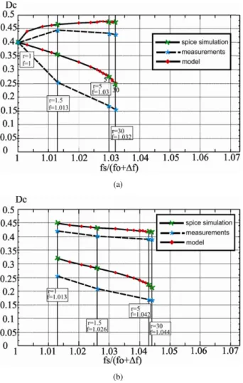
Figure 22 shows the comparison among the model, the SPICE simulation and the experimetal results for the global duty cycle window. Four different loads were selected for the measuremets. Figure 22a shows the results for the maximum gain at Vcc=120V, while the Figure 22b ilustrates the results for an intermediate gain at Vcc=180V. It can be seen a small deviation on the experimental curves. However, there is al-ways a common region between model and measurements. The results induce to the conclusion that the duty cycle func-tion should be implemented near to the lower curve given by the model. This would guarantee ZVS for all operation range.
Table 2: Parameter of the Implemented Converter.
Parameter Value Unit Vin_ac 85-260 V fs 155...172 kHz
Vo_rms 6 V
Po 3 W
Q1 30.7-61.4-480
-RL 12-44-360 Ω
Table 3: Experimental results for Vcc=200V.
fs Applied Dc
Dc
window Vo_rms 157kHz 0.4 0.4 12.5 166kHz 0.15 0.05-0.28 3.7
(a)
(b)
Figure 21: Results comparison between theory and experi-ments. (a) Duty cycle window. (b) Gain Vo/Vin.
(a)
(b)
Figure 22: Experimental results of the global duty cycle win-dow. (a) For minimum input voltage, Vcc=120V. (b) For 1.5 times the minimum voltage, Vcc=180V.
It is important to point out that the small deviation between the theory and experimental results are given by neglected parasitic components. One of the simplifications is the effi-ciency of the transformer, which is considered as unity. A parasitic element that influences a lot the circuit is the switch capacitance. The probes capacitance interfere as well, and can be considered in future works.
6
CONCLUSIONS
This paper shows an extension on how to analyze resonant converters based on a normalized methodology. The theory was applied to the Class-E topology with piezoelectric trans-formers, due to the promising characteristics of this combi-nation, as reduced size, weight, etc.
Former papers introduced the normalized method to design the nominal point of the converters, regardingless the overall operation range.
The whole operation range was considered in this work. The switching frequency and the load where sweeped to obtain the global duty cycle window of the circuit. This window de-fines which duty cycles should be applied for each switching frequency in order to obtain ZVS. This information is used to implement the modulator and is called duty cycle tracking .
These results allow to achieve the optimum desing point which considers the complete operation of the converter, in-cluding frequencies and loads.
The methodology was validated experimentally with a 3W step-down prototype. It was designed for universal input, 85-260 V AC, and an output of 6 V DC.
The SPICE simulation and the mathematical model are com-pletely in agreement. The model and experimental results are in agreement with a small deviation given by neglected para-sitic components. The results help to understand the complex behavior of such a converter.
REFERENCES
Bisogno, F.E, Radecker, M. And Knoll, A. (2004). Com-parison of Resonant Topologies for Step-Down Appli-cations Using Piezoelectric Transformers. IEEE Power Electronics Specialists Conference, Vol. 4, pp 2662-2667
Bisogno, F.E, Radecker, M. and Nittayarumphong, S. (2005). Dynamical Modeling of Class-E Resonant Con-verter for Step-Down Applications Using Piezoelectric Transformers.IEEE Power Electronics Specialists Con-ference, pp 2797-2803.
Bisogno, F.E, Nittayarumphong, S, Radecker, M, Carazo, A. V. and do Prado, R. N. (2006). A line Power-Supply for LED Lighting using Piezoelectric Transformers in Class-E- Topology. International Power Electronics and Motion Control Conference, Vol 2, pp. 1-5.
Bisogno, F. E. (2006). Energy related system normalization and decomposition targeting sensitivity consideration. PhD. Dissertation, Dept. Elektrotechnik und Informa-tionstechnik. Eng., Univ. der Technischen Universität Chemnitz Zwickau.
Diaz J, Nuño, F, Lopera J M, Martin-Ramos, J. A. (2001). A New Confrol Strategy for an AC/DC Converter Based on a Piezoelectric Transformer. IEEE Transaction on Industrial Electronics, Vol. 51, Issue 4, pp. 850-856.
Kazimierczuk, M. K. and Puczko, K (1987). Exact Anal-ysis of Class E Tuned Power Amplifier at any Q and Switch Duty Cycle. IEEE Transactions in Circuits and Systems, Vol. 34, No 2, pp 149-159.
Lin, C. Y. (1997). Design and Analysis of Piezoelectric Transformer Converters. Ph.D. Dissertation, Virgínia Tech.
Ninomiya, T, Shoyama, M, Zaitsu, T. and Inoue, T. (1994). Zero-Voltage-Switching Techniques and their Applica-tion to High-Frequency Converter with Piezoelectric Transformer. Control and Instrumentation Industrial Electronics, Vol 3, pp. 1665-1669.
Nittayarumphong, S, Bisogno, F.E, Radecker, M,Knoll, A, , Riedlhammer, A. and Carazo, A. V. (2005). Dynamic behaviour of PI controlled Class-E Resonant Converter for Step-Down Applications Using Piezoelectric Trans-formers. European conference on Power Electronics Applications, pp 10.
Nittayarumphong, S, Bisogno, F. E. and Radecker, M. (2006). Comparison of Control Concepts for Off-Line Power Supplies using Piezoelectric Transformers in Class-E Topology.IEEE Power Electronics Especial-ist Conference, pp 1-7.
Prieto, M. J, Díaz, J. A, Martín, J. A. and Nuño, F. (2001). A very simple DC/DC Converter Using Piezoelectric Transformer.IEEE Power Electronics Especialist Con-ference, Vol 4, pp. 1755-1760.
Shoyama, M, Horikoshi, K, Ninomiya, T, Zaitsu, T, Sasaki, Y. (1997). Steady-State Characteristics of the Push-pull Piezoelectric Inverter.IEEE Power Electronics Special-ists Conference, Vol. 1, pp 715-721.
Yang, Q, Bing, L, Bo, Y, Dianbo, F, Lee, F. C, Canales, F, Gean, R, Tipton, W. C. (2004). A frequency, high-efficiency three-level LCC converter for high-voltage charging applications.IEEE Power Electronics Special-ists Conference, Vol. 6, pp 4100-4106.
Yang, Y, Bisogno, F. E, Schittler, A, Nittayarumphong, S, Radecker, M. (2009). Comparison of Inductor-Half-Bridge and Class-E Resonant Topologies for Piezo-electric Transformer Applications. Energy Conversion Congress and Exposition, pp 776-782.
Yamane, T, Hamamura, S, Zaitsu, T, Ninomiya, T, Shoyama, M. and Fuda, Y (1998) . Efficiency Im-provement of Piezoelectric-transformer DC-DC Con-verter.IEEE Power Electronics Specialists Conference, Vol. 2, pp 1255-1261.