Braz. J. of Develop.,Curitiba, v. 6, n. 10, p. 79016-79040, oct. 2020. ISSN 2525-8761
Design of a Fully Digital GMSK Demodulator for Telemetry Space Link
Projeto de Demodulador Completamente Digital para Enlace de Telemetria
Espacial
DOI:10.34117/bjdv6n10-364
Recebimento dos originais: 10/09/2020 Aceitação para publicação: 16/10/2020
Antonio Macilio Pereira de Lucena
Doutor em Engenharia de Teleinformática pela Universidade Federal do Ceará (UFC) Instituição: Instituto Nacional de Pesquisas Espaciais (INPE) e Universidade de Fortaleza (Unifor)
Endereço: Rua Estrada do Fio, 5624-6140 - Mangabeira, Eusébio - CE, 61760-000 Email: antonio.lucena@inpe.br
Paulo Daving Lima de Oliveira
Mestre em Engenharia Elétrica pela Universidade Federal do Ceará (UFC) Instituição: Instituto Nacional de Pesquisas Espaciais (INPE)
Endereço: Rua Estrada do Fio, 5624-6140 - Mangabeira, Eusébio - CE, 61760-000 Email: daving@dee.ufc.br
Francisco de Assis Tavares Ferreira da Silva
Doutor em Computação pelo Instituto Nacional de Pesquisas Espaciais (INPE) Instituição: Instituto Nacional de Pesquisas Espaciais (INPE)
Endereço: Rua Estrada do Fio, 5624-6140 - Mangabeira, Eusébio - CE, 61760-000 Email: francisco.silva@inpe.br
ABSTRACT
This paper presents the design of a coherent GMSK demodulator, with fully digital architecture, aimed at high speed (10 Mbps) space telemetry applications in which the absolute Doppler offset may reach up to 200 kHz. All functional modules that compose the demodulator are described through block diagrams and mathematical equations. The calculations for the determination of several design parameters are presented. The carrier phase and the symbol timing recovery modules are distinct from those found in the literature for this application and, therefore, original mathematical analysis for the project of such modules are performed. The performance of the proposed GMSK demodulator is evaluated via computational simulation. Besides the bit error rate under several operating conditions, the variance of the estimated parameters by the symbol and carrier synchronizers are measured and compared with theoretical bounds. The main results from computational simulations are presented and demonstrate remarkable performance of the designed demodulator.
Keywords: GMSK; Demodulator; Telemetry; Fully digital; Space communications. RESUMO
Este trabalho apresenta o projeto de um demodulador GMSK coerente, com arquitetura totalmente digital, voltado para aplicações de telemetria espacial de alta velocidade (10 Mbps) em que desvio Doppler absoluto pode atingir até 200 kHz. Todos os módulos funcionais que compõem o demodulador são descritos por meio de diagramas de blocos e equações matemáticas. Os cálculos para a determinação dos vários parâmetros de projeto são apresentados. Os módulos para a recuperação da
Braz. J. of Develop.,Curitiba, v. 6, n. 10, p. 79016-79040, oct. 2020. ISSN 2525-8761
fase da portadora e para a temporização de símbolos são distintos daqueles encontrados na literatura e, portanto, as análises matemáticas apresentadas para o projeto de tais módulos são originais. O desempenho do demodulador GMSK proposto é avaliado por simulação computacional. Além da taxa de erro de bit, sob várias condições operacionais, a variância dos parâmetros estimados pelos sincronizadores de símbolo e de portadora são medidos e comparados com limites teóricos. Os principais resultados das simulações computacionais são apresentados, demonstrando um notável desempenho do demodulador proposto.
Palavras chaves: GMSK, Demodulador, Telemetria, Completamente digital, Telecomunicação
espacial.
1 INTRODUCTION
Gaussian Minimum Shift Keying (GMSK) modulation [1] reveals good performance in terms of bit error rate (BER), great spectral efficiency, and, due to its constant-envelope nature, it can be employed in channels with nonlinear amplifiers, operating in quasi-saturation, without significant distortion added to the modulated signal [2, 3]. Due to these characteristics, the pre-coded GMSK modulation is recommended by the Consultative Committee for Space Data Systems (CCSDS) for high speed telemetry links under all mission categories for space research and earth exploration [4].
It is presented in this paper the design of a GMSK demodulator with bandwidth-time product of 0.25 (BT=0.25), high transmission rate (10 Mbps), fully compliant with CCSDS recommendations and aimed at space telemetry for near-Earth missions. The developed demodulator is entirely digital and operates on the discrete GMSK samples at the IF (Intermediate Frequency) stage, where the carrier frequency is 70 MHz.
There are some articles in the literature that present coherent GMSK demodulator designs detailing the structures for carrier recovery, symbol synchronism and bit detection [5-7] in the same way as in this work. However, our proposal is distinguished in several aspects. First, the architecture is capable of supporting Doppler shifts within ±200 kHz, in compliance with S-band transmissions, because, in addition to the carrier phase synchronizer, there is an exclusive module for frequency offset estimation. The solutions described in [5-7] use solely a phase recovery loop that is only able to estimate a little frequency offset. The capability of the proposed demodulator in operating at large frequency offsets allows significant simplification in the design of the receiver at the ground station, since the conversion of the received signal to the IF stage can be performed with a simple open-loop local oscillator [8].
Although the designed demodulator has a linear architecture, based on Laurent's representation, and uses a Wiener filter for signal equalization prior to detection, exactly as described in [5], the adopted carrier phase synchronizer and symbol synchronizer inside the demodulator are different from
Braz. J. of Develop.,Curitiba, v. 6, n. 10, p. 79016-79040, oct. 2020. ISSN 2525-8761
those presented in [5-7]. The carrier phase is recovered through a discrete closed-loop configuration, which implements a Costas loop distinct to those discussed in [5,6,9]. In our case, the configuration is simpler and there is no need for symbol synchronization for the loop to work. We will demonstrate that the adopted solution is suitable for phase recovery of GMSK signals and present some unprecedented mathematical analysis to explain its functioning.
The proposed architecture for the bit synchronization module is also less complex than the solution given in [5-7] and is based on a discrete version of the delay-line multiplier synchronizer [10, 11] with an additional linear interpolator. As far as the authors are concerned, this type of synchronizer has never been used in GMSK demodulation. Despite its simplicity, as shown in the results section, the performance is well satisfactory.
This paper is organized as follows: In section 2, it is presented in detail the design and operation of the demodulator through block diagrams and equations. Some mathematical analysis necessary to the project development are also presented in that section. The results of computational simulations for the system performance, with some discussions, are provided in section 3. Concluding remarks are given in section 4.
2 PROJECT DESCRIPTION
2.1 SIGNAL MODEL
CCSDS [4] recommends a data pre-coding scheme for the transmitted symbols, performed before the GMSK modulation, in order to eliminate the inherent differential coding of continuous-phase modulations. On doing so, there is a reduction by a factor of two in the bit error rate. The pre-coded symbol, denoted by 𝑎[𝑘], transmitted at the k-th instant is determined by the expression 𝑎[𝑘] = (−1)𝑘𝑑[𝑘]𝑑[𝑘 − 1] , in which 𝑑[𝑘] ∈ {1, −1} represents the k-th non-coded symbol to be transmitted.
The GMSK signal at the output of the intermediate frequency stage of the receiver, can be approximated by the following equation [4, 9]:
Braz. J. of Develop.,Curitiba, v. 6, n. 10, p. 79016-79040, oct. 2020. ISSN 2525-8761 𝑟(𝑡) = √2𝐸𝑏 𝑇 ∑ { ∞ 𝑘=−∞ 𝑑[2𝑘]𝐶0(𝑡 − 2𝑘𝑇 − 𝜏) − 𝑑[2𝑘 − 1]𝑑[2𝑘]𝑑[2𝑘 + 1]𝐶1(𝑡 − 2𝑘𝑇 − 𝑇 − 𝜏)} cos[2𝜋(𝑓𝐼𝐹+ 𝑓𝑑)𝑡 + 𝜃] + {𝑑[2𝑘 + 1]𝐶0(𝑡 − 2𝑘𝑇 − 𝑇 − 𝜏) − {𝑑[2𝑘]𝑑[2𝑘 − 1]𝑑[2𝑘 − 2]𝐶1(𝑡 − 2𝑘𝑇 − 𝜏) + {𝑑[2𝑘 + 1]𝐶0(𝑡 − 2𝑘𝑇 − 𝑇 − 𝜏)} sin[2𝜋(𝑓𝐼𝐹+ 𝑓𝑑)𝑡 + 𝜃] + 𝑤(𝑡), (1)
where 𝐸𝑏 corresponds to the energy per bit; 𝑇 is the bit duration; 𝑑[𝑙] is the non-coded symbol transmitted at the l-th period,
with 𝑙 being an integer; 𝑓𝐼𝐹, equal to 70 MHz, is the intermediate frequency of the receiver; 𝑓𝑑 is the carrier frequency offset
due to the Doppler effect and to the lack of synchronization between transmitter and receiver; 𝜃 is an unknown phase; and 𝜏 is the propagation delay of the symbol. 𝐶0(𝑡) and 𝐶1(𝑡) are the first two amplitude modulation pulses of Laurent’s
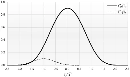
decomposition [12, 13] for the GMSK signal. Figure 1 shows the waveform of both pulses for the present case in which
BT=0.25.
Figure 1. C0(t) and C1(t) pulses for GMSK signals with BT = 0.25.
The symbols referenced in Eqn (1) as 𝑑[2𝑘] and 𝑑[2𝑘 + 1], that convey the information to be recovered, multiply 𝐶0(𝑡). In contrast, the terms involving 𝐶1(𝑡) in Eqn (1) represent intersymbol interference (ISI) in the detection process.
The amount of noise in the received signal 𝑟(𝑡), denoted by 𝑤(𝑡), is modeled as a white random bandpass Gaussian process, centered at 𝑓𝐼𝐹, bandwidth 2𝑊 equal to 20 MHz, with zero-mean and power spectral density of 𝑁0/2.
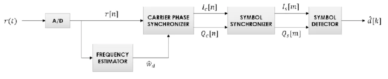
Braz. J. of Develop.,Curitiba, v. 6, n. 10, p. 79016-79040, oct. 2020. ISSN 2525-8761 2.2 FUNCTIONAL ARCHITECTURE OF THE GMSK DEMODULATOR
The functional block diagram of the developed demodulator is shown in Figure 2. The analog signal 𝑟(𝑡) is processed by an A/D converter generating its digital version 𝑟[𝑛] . The frequency estimator, taking the discrete signal 𝑟[𝑛], determines and delivers to the carrier phase synchronizer the digital frequency estimate 𝑤̂𝑑 corresponding to the frequency offset 𝑓𝑑 of the received signal defined
by Eqn (1). The carrier phase synchronizer, in turn, synthesize sine and cosine waveforms with the same phase and frequency of the carrier associated to 𝑟[𝑛] so that proper conversion can be done to obtain the baseband signals 𝐼𝑐[𝑛] and 𝑄𝑐[𝑛]. Thus, this module provides the phase recovery and eventually performs the synchronization of some residual frequency offset due to the error in the 𝑤̂𝑑
estimate. The symbol synchronizer interpolates and picks the best samples from the signals 𝐼𝑐[𝑛] and 𝑄𝑐[𝑛] for each received symbol, and presents to the symbol detector module these synchronized baseband signals 𝐼𝑠[𝑚] and 𝑄𝑠[𝑚] at a rate of 1/2𝑇. Finally, the symbol detector module equalizes
𝐼𝑠[𝑚] and 𝑄𝑠[𝑚] before performing the symbol detection and the generation of the estimates 𝑑̂[𝑘] of the non-coded GMSK symbols that have been transmitted.
Figure 2. Functional block diagram of the GMSK demodulator.
In the next sections, the design of every functional module of the GMSK demodulator is presented in detail.
2.3 A/D CONVERTER
The A/D conversion is performed on the bandpass signal 𝑟(𝑡) derived from the IF stage. Considering the characteristics of 𝑟(𝑡), the smallest sampling frequency necessary to avoid aliasing is 𝑓𝑠 = 40 MHz [14]. The discrete signal at the output of the converter, denoted by 𝑟[𝑛] = 𝑟(𝑛𝑇𝑠), with 𝑇𝑠 = 1/𝑓𝑠 being the sample period and 𝑛 the sample index, may be expressed by 𝑟[𝑛] =
Braz. J. of Develop.,Curitiba, v. 6, n. 10, p. 79016-79040, oct. 2020. ISSN 2525-8761 where 𝑤𝐼𝐹 = 2𝜋𝑓𝐼𝐹/𝑓𝑠 = 7𝜋/2, 𝑤𝑑 = 2𝜋𝑓𝑑/𝑓𝑠, 𝐼[𝑛] = √2𝐸𝑏 𝑇 ∑ { ∞ 𝑘=−∞ 𝑑[2𝑘]𝐶0(𝑛𝑇𝑠− 2𝑘𝑇 − 𝜏) − 𝑑[2𝑘 − 1]𝑑[2𝑘]𝑑[2𝑘 + 1]𝐶1(𝑛𝑇𝑠− 2𝑘𝑇 − 𝑇 − 𝜏)}, (3) and 𝑄[𝑛] = √2𝐸𝑏 𝑇 ∑ { ∞ 𝑘=−∞ 𝑑[2𝑘 + 1]𝐶0(𝑛𝑇𝑠 − 2𝑘𝑇 − 𝑇 − 𝜏) − 𝑑[2𝑘]𝑑[2𝑘 − 1]𝑑[2𝑘 − 2]𝐶1(𝑛𝑇𝑠− 2𝑘𝑇 − 𝜏)}. (4)
The signal 𝑤[𝑛] is the result of the discretization of the Gaussian noise 𝑤(𝑡), i. e., 𝑤[𝑛] = 𝑤(𝑛𝑇𝑠). From the characteristics of 𝑤(𝑡) described in Section 2.1, the corresponding autocorrelation function of 𝑤(𝑡) is given by [15]
𝑅𝑤(𝛾) = 2𝑁0𝑊𝑠𝑖𝑛𝑐(2𝑊𝛾)𝑐𝑜𝑠(2𝜋𝑓𝐼𝐹𝛾). (5)
Therefore, the autocorrelation function of 𝑤[𝑛], denoted by 𝑅𝑤[𝑢], is derived from Eqn (5) taking 𝛾 = 𝑢𝑇𝑠 and 2𝑊 = 𝑓𝑠/2. The resulting equation is
𝑅𝑤[𝑢] = 𝑁0 2𝑇𝑆𝑠𝑖𝑛𝑐 ( 𝑢 2) 𝑐𝑜𝑠 ( 7𝜋𝑛 2 ) = 𝑁0 2𝑇𝑆𝛿[𝑢], (6)
where 𝛿[𝑢] is the discrete unit impulse signal. It is noticeable from Eqn (6) that the Gaussian noise 𝑤[𝑛] is also white. In this work, the effects of quantization are taken as negligible when compared to the Gaussian noise 𝑤[𝑛].
2.4 FREQUENCY ESTIMATOR
CCSDS [16] recommends that the receivers in telemetry links for category A missions (altitude less than 2x10⁶ km) and operating in the S-band, which is the case of this project, must be able to support Doppler shifts of up to ±150 kHz.
The frequency estimator receives the discrete GMSK signal 𝑟[𝑛] and, from it, makes an estimate of the digital frequency offset 𝑤𝑑 that may vary within the interval corresponding to -200 kHz ≤ 𝑓𝑑 ≤ 200 kHz to comply, with considerable slack, with the requirements imposed by the CCSDS
Braz. J. of Develop.,Curitiba, v. 6, n. 10, p. 79016-79040, oct. 2020. ISSN 2525-8761
recommendations. For the proposed estimator, the error in the estimates, given by |𝑤̂𝑑− 𝑤𝑑|, is below the analog frequency corresponding to 50 Hz. The fine-tune synchronization of the frequency is fulfilled by the carrier phase synchronizer with the information of 𝑤̂𝑑.
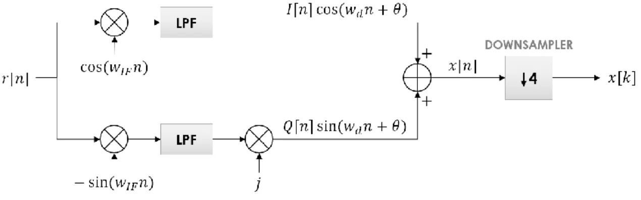
The block diagram of the frequency estimator is presented in Figure 3. The frequency estimate is derived out of the first 215 samples of 𝑟[𝑛] at the beginning of the reception. As indicated in Fig. 3, assuming 𝑤[𝑛] negligible, the input signal 𝑟[𝑛] with carrier frequency of (𝑤𝐼𝐹+ 𝑤𝑑) is down-converted into the complex signal 𝑥[𝑘], with carrier frequency 𝑤𝑑, given by the following equation:
𝑥[𝑘] = 𝐼[𝑘] cos(𝑤𝑑𝑘 + 𝜃) + 𝑗𝑄[𝑘] sin(𝑤𝑑𝑘 + 𝜃). (7)
Figure 3. Block diagram of the frequency estimator module.
The operations performed by the low-band converter module are depicted in figure 4. This module implements a classical quadrature down-converter with oscillators at the frequency w_if. In fact, the real frequency of oscillators is not exactly w_if. There are some frequency offset and phase offset that are incorporated by the values of w_d and θ, respectively. The low-band signals, at the outputs of the low-pass filters (lpf), are combined and decimated by 4 to build the complex signal x[k]. The low-pass filters are digital approximations of butterworth, with cutoff frequencies equivalent to the analog frequencies of 10 mhz.
Braz. J. of Develop.,Curitiba, v. 6, n. 10, p. 79016-79040, oct. 2020. ISSN 2525-8761
The signal 𝑥[𝑘] is nothing but a discrete version of the baseband counterpart of the GMSK signal received and shifted to the frequency 𝑤𝑑. Hence, 𝑥[𝑘] does not contain any spectral component at the carrier frequency.
The processing of 𝑥[𝑘] through a quadratic non-linerity, described by 𝑦[𝑘] = (−1)𝑘𝑥2(𝑘) (8),
causes the emergence of a spectral component in 𝑦[𝑘] at the frequency 2𝑤𝑑, as demonstrated in the literature [17, 18]. If the fractions of inter-symbol interference (ISI) and Gaussian noise present in 𝑟[𝑛] were negligible, the signal 𝑦[𝑘] would be a complex exponential with frequency equal to 2𝑤𝑑 [17]. In the non-ideal case, the power spectrum of 𝑦[𝑘] is basically a spectral component at 2𝑤𝑑 immersed in a continuous spectrum due to ISI and noise.
As shown in Figure 3, the 𝑤𝑑 estimate is performed by the use of the discrete Fourier transform
(DFT) following the steps:
1) Find the DFT of 𝑦[𝑘] within M = 212 points using N = 213 samples of such signal. The
DFT is calculated by the expression:
DFT{𝑦[𝑘]} = 𝑌[𝑝] = ∑ 𝑦[𝑘]𝑒−𝑗 2𝜋 𝐿𝑝𝑘, −𝑀 2 ≤ 𝑝 ≤ 𝑀 2 − 1, 𝑁−1 𝑘=0 (9)
where L = 5x10⁴. Therefore, the 𝑌[𝑝] samples are separated by 2𝜋/𝐿 rad, which corresponds to a distance of 200 Hz in
terms of analog frequency. This way, the analog frequency interval encompassed by the 𝑌[𝑝] samples starts from -409.6 kHz (𝑝 = −𝑀/2) up to 409.4 kHz (𝑝 = 𝑀/2 − 1).
2) Determine which sample 𝑌[𝑝𝑚] corresponds to the maximum value of |𝑌[𝑝]|. From that, the estimated frequency will be 𝑤̂𝑑 = 𝜋𝑝𝑚/𝐿.
2.5 CARRIER PHASE SYNCHRONIZER
The main functions of this module are the carrier phase synchronization and the conversion of the GMSK signal to baseband. The adopted architecture is capable of recovering the phase even when it varies, thus, as previously mentioned, the fine-tune frequency synchronization is performed by this module.
The solution is based on the decision-directed phase recovery technique [19] and has been implemented as a discrete Costas loop. The proposed architecture differs from those phase recovery loops for GMSK signals found in the literature [5-7,9] and [19, 20]. The adopted loop is fully discrete, operates at a sampling rate 𝑓𝑠 = 4/𝑇 and does not require symbol synchronization to properly work,
Braz. J. of Develop.,Curitiba, v. 6, n. 10, p. 79016-79040, oct. 2020. ISSN 2525-8761
which allows significant simplification. Costas loop with similar structures, that do not need symbol synchronization, have been described in references [21-24] as a solution for phase recovery in QPSK modulation. In this work, it is presented a detailed description of this type of loop for GMSK signals and, additionally, some original mathematical analysis.
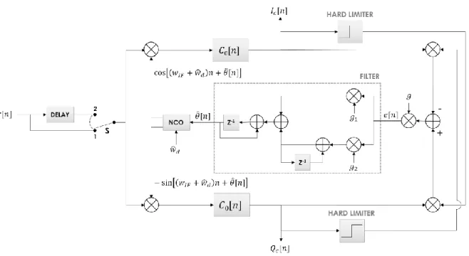
The block diagram of the carrier phase synchronizer module is depicted in Figure 5. The set composed by the delay block and the switch S at the input of the loop is used so that no symbol is lost during the synchronization phase of the demodulator. At the beginning of the reception, the switch S is in the position 1. After certain number of samples, corresponding to the length of the delay chain, when frequency, phase and symbol synchronization have already been retrieved, the switch is changed to position 2 and, from that instant on, the detected symbols start to be accepted.
Figure 5. Block diagram of the carrier phase synchronizer module.
The remainder of the circuit implements a discrete Costas loop. The input signal 𝑟[𝑛] is multiplied on both mixers, and the converted signals are filtered on the arms I and Q of the loop by low-pass filters whose the impulsive response is 𝐶0[𝑛] = 𝐶0(𝑛𝑇𝑠), both for suppressing the second
harmonic and for the matching with the transmitted pulse. The resulting signals 𝐼𝑐[𝑛] and 𝑄𝑐[𝑛] are used to generate an error signal 𝑒[𝑛] as well as for later symbol synchronization and detection. Inside the loop, the error signal 𝑒[𝑛], after filtered by the loop filter, controls the phase and frequency of the sine/cosine waveforms that have been generated by the numeric-controlled oscillator and used to close the loop via both input mixers.
Braz. J. of Develop.,Curitiba, v. 6, n. 10, p. 79016-79040, oct. 2020. ISSN 2525-8761
Since the authors have not found in the literature a detailed analysis about how this loop structure for GMSK signals works, it will be presented, as follows, an analytical development for the determination of the S-curve of the phase detector.
Determination of the S-curve
Neglecting the Gaussian noise in Eqn (2) and supposing the frequency synchronization (𝑤̂𝑑 = 𝑤𝑑), the signals at the output of the low-pass filters 𝐶0[𝑛], on each arm of the loop, are
𝐼𝑐[𝑛] = 𝐼[𝑛] ∗ 𝐶0[𝑛]𝑐𝑜𝑠𝜙[𝑛] − 𝑄[𝑛] ∗ 𝐶0[𝑛]𝑠𝑖𝑛𝜙[𝑛], (10)
𝑄𝑐[𝑛] = 𝐼[𝑛] ∗ 𝐶0[𝑛]𝑠𝑖𝑛𝜙[𝑛] + 𝑄[𝑛] ∗ 𝐶0[𝑛]𝑐𝑜𝑠𝜙[𝑛], (11)
in which (*) indicates the convolution operation, 𝐶0[𝑛] is the discrete version of the first pulse in Laurent’s decomposition,
and 𝜙[𝑛] = 𝜃 − 𝜃̂[𝑛]. Furthermore, considering negligible the pulse 𝐶1(𝑡) in Eqns (3) and (4), 𝑇/𝑇𝑠= 4 and 𝜏 = 0, we
have 𝐼[𝑛] ∗ 𝐶0[𝑛] = √ 2𝐸𝑏 𝑇 ∑ 𝑑[2𝑘]𝑃[𝑛 − 8𝑘] ∞ 𝑘=−∞ , (12) 𝑄[𝑛] ∗ 𝐶0[𝑛] = √2𝐸𝑏 𝑇 ∑ 𝑑[2𝑘 + 1]𝑃[𝑛 − 8𝑘 − 4] ∞ 𝑘=−∞ , (13)
Where the discrete pulse P[n] is given by 𝐶0[𝑛] ∗ 𝐶0[𝑛] and is plotted in figure 6.
Figure 6. discrete pulse shape at the output of the c0[n] filter.
The pulse 𝑃[𝑛] with 41 taps may be expressed as a vector by the following equation 𝑃[𝑛] = [𝑝−20, 𝑝−19, … , 𝑝−1, 𝑝0, 𝑝1, … , 𝑝19, 𝑝20] (14) , being 𝑝0 = 𝑃[0] , the central tap and the maximum
Braz. J. of Develop.,Curitiba, v. 6, n. 10, p. 79016-79040, oct. 2020. ISSN 2525-8761
Figure 7 shows three pulses (k=-1, 0, 1) at the output of the low-pass filter on the I-arm of the loop that correspond to the sum in Eqn (12), for the case where 𝑑[−2] = 1, 𝑑[0] = 1 and 𝑑[2] = −1.
Figure 7. The first three pulses at the output of the filter on the I-ARM
.
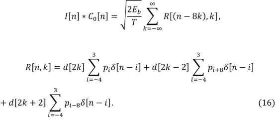
Taking the second pulse (k=0) as a reference, it is easy to observe that: a) the amplitudes of the central samples in the second pulse (from 𝑛 = −4 to 𝑛 = 3) are greater than or equal to the amplitudes of the interfering samples; b) only neighboring pulses, specifically the first and third pulses, contribute with non-zero ISI to the central samples. As a result, one can restate Eqn (12), valid in the following way: 𝐼[𝑛] ∗ 𝐶0[𝑛] = √ 2𝐸𝑏 𝑇 ∑ 𝑅[(𝑛 − 8𝑘), 𝑘] ∞ 𝑘=−∞ , (15) in which 𝑅[𝑛, 𝑘] = 𝑑[2𝑘] ∑ 𝑝𝑖𝛿[𝑛 − 𝑖] 3 𝑖=−4 + 𝑑[2𝑘 − 2] ∑ 𝑝𝑖+8𝛿[𝑛 − 𝑖] 3 𝑖=−4 + 𝑑[2𝑘 + 2] ∑ 𝑝𝑖−8𝛿[𝑛 − 𝑖] 3 𝑖=−4 . (16)
It is noticeable that the first term in Eqn (16) represents the central samples of the k-th pulse, while the second and third terms are ISI due to the pulses at instants 𝑘 − 1 and 𝑘 + 1. It is also clear that there is no overlap between the pulses 𝑅[(𝑛 − 8𝑘), 𝑘] in the sum of Eqn (15).
Braz. J. of Develop.,Curitiba, v. 6, n. 10, p. 79016-79040, oct. 2020. ISSN 2525-8761 𝑄[𝑛] ∗ 𝐶0[𝑛] = √2𝐸𝑏 𝑇 ∑ 𝑆[(𝑛 − 8𝑘 − 4), 𝑘] ∞ 𝑘=−∞ , (17) in which 𝑆[𝑛, 𝑘] = 𝑑[2𝑘 + 1] ∑ 𝑝𝑖𝛿[𝑛 − 𝑖] 3 𝑖=−4 + 𝑑[2𝑘 − 1] ∑ 𝑝𝑖+8𝛿[𝑛 − 𝑖] 3 𝑖=−4 + 𝑑[2𝑘 + 3] ∑ 𝑝𝑖−8𝛿[𝑛 − 𝑖] 3 𝑖=−4 . (18)
Rewriting Eqns (10) and (11), considering the new formulation of Eqns (15) and (17), we have:
𝐼𝑐[𝑛] = √ 2𝐸𝑏 𝑇 {cos𝜙[𝑛] ∑ 𝑅[(𝑛 − 8𝑘), 𝑘] ∞ 𝑘=−∞ − 𝑠𝑖𝑛𝜙[𝑛] ∑ 𝑆[(𝑛 − 8𝑘 − 4), 𝑘]} ∞ 𝑘=−∞ , (19) 𝑄𝑐[𝑛] = √ 2𝐸𝑏 𝑇 {sin𝜙[𝑛] ∑ 𝑅[(𝑛 − 8𝑘), 𝑘] ∞ 𝑘=−∞ + 𝑐𝑜𝑠𝜙[𝑛] ∑ 𝑆[(𝑛 − 8𝑘 − 4), 𝑘]} ∞ 𝑘=−∞ , (20)
Assuming that the phase error 𝜙[𝑛] in Eqns (19) and (20) are small and taking the pulse samples shown in Figure 7 as a reference, the signals at the output of the limiters are given by
𝑆𝑔𝑛{𝐼𝑐[𝑛]} = ∑ 𝑇[(𝑛 − 8𝑘), 𝑘] ∞ 𝑘=−∞ , (21) 𝑆𝑔𝑛{𝑄𝑐[𝑛]} = ∑ 𝑈[(𝑛 − 8𝑘 − 4), 𝑘] ∞ 𝑘=−∞ , (22) in which 𝑇[𝑛, 𝑘] = (𝑑[2𝑘] 2 + 𝑑[2𝑘 − 2] 2 ) 𝛿[𝑛 + 4] + 𝑑[2𝑘] ∑ 𝛿[𝑛 − 𝑖] 3 𝑖=−3 , (23) 𝑈[𝑛, 𝑘] = (𝑑[2𝑘 + 1] 2 + 𝑑[2𝑘 − 1] 2 ) 𝛿[𝑛 + 4] + 𝑑[2𝑘 + 1] ∑ 𝛿[𝑛 − 𝑖] 3 𝑖=−3 . (24)
Braz. J. of Develop.,Curitiba, v. 6, n. 10, p. 79016-79040, oct. 2020. ISSN 2525-8761 Following the signal flow in Figure 6, we have
𝑒[𝑛] = 𝑔(𝑄𝑐[𝑛]𝑠𝑔𝑛{𝐼𝑐[𝑛]} − 𝐼𝑐[𝑛]𝑠𝑔𝑛{𝑄𝑐[𝑛]}), (25)
where 𝑔 is a gain used to normalize the error. Replacing Eqns (19), (20), (21) and (22) in Eqn (25), and doing some algebraic manipulations, result in
𝑒[𝑛] = √2𝐸𝑏
𝑇 𝑔sin𝜙[𝑛] ∑ {𝑅[(𝑛 − 8𝑘), 𝑘]𝑇[(𝑛 − 8𝑘), 𝑘]
∞
𝑘=−∞
+ 𝑆[(𝑛 − 8𝑘 − 4), 𝑘]𝑈[(𝑛 − 8𝑘 − 4), 𝑘]}. (26)
From Eqns (16), (18), (23) and (24), we have
𝑅[𝑛, 𝑘]𝑇[𝑛, 𝑘] = [(1 2+ 𝑑[2𝑘]𝑑[2𝑘 − 2] 2 ) 𝑝−4+ ( 1 2+ 𝑑[2𝑘]𝑑[2𝑘 − 2] 2 ) 𝑝4 + (𝑑[2𝑘]𝑑[2𝑘 + 2] 2 + 𝑑[2𝑘 − 2]𝑑[2𝑘 + 2] 2 ) 𝑝−12] 𝛿[𝑛 + 4] + (𝑝−3+ 𝑑[2𝑘]𝑑[2𝑘 − 2]𝑝5 + 𝑑[2𝑘]𝑑[2𝑘 + 2]𝑝−11)𝛿[𝑛 + 3] + (𝑝−2+ 𝑑[2𝑘]𝑑[2𝑘 − 2]𝑝6+ 𝑑[2𝑘]𝑑[2𝑘 + 2]𝑝−10)𝛿[𝑛 + 2] + (𝑝−1+ 𝑑[2𝑘]𝑑[2𝑘 − 2]𝑝7+ 𝑑[2𝑘]𝑑[2𝑘 + 2]𝑝−9)𝛿[𝑛 + 1] + (𝑝0+ 𝑑[2𝑘]𝑑[2𝑘 − 2]𝑝8 + 𝑑[2𝑘]𝑑[2𝑘 + 2]𝑝−8)𝛿[𝑛] + (𝑝1+ 𝑑[2𝑘]𝑑[2𝑘 − 2]𝑝9+ 𝑑[2𝑘]𝑑[2𝑘 + 2]𝑝−7)𝛿[𝑛 − 1] + (𝑝2 + 𝑑[2𝑘]𝑑[2𝑘 − 2]𝑝10+ 𝑑[2𝑘]𝑑[2𝑘 + 2]𝑝−6)𝛿[𝑛 − 2] + (𝑝3+ 𝑑[2𝑘]𝑑[2𝑘 − 2]𝑝11 + 𝑑[2𝑘]𝑑[2𝑘 + 2]𝑝−5)𝛿[𝑛 − 3], (27) and
Braz. J. of Develop.,Curitiba, v. 6, n. 10, p. 79016-79040, oct. 2020. ISSN 2525-8761 𝑆[𝑛, 𝑘]𝑈[𝑛, 𝑘] = [(1 2+ 𝑑[2𝑘 + 1]𝑑[2𝑘 − 1] 2 ) 𝑝−4+ ( 1 2+ 𝑑[2𝑘 + 1]𝑑[2𝑘 − 1] 2 ) 𝑝4 + (𝑑[2𝑘 + 1]𝑑[2𝑘 + 3] 2 + 𝑑[2𝑘 − 1]𝑑[2𝑘 + 3] 2 ) 𝑝−12] 𝛿[𝑛 + 4] + (𝑝−3 + 𝑑[2𝑘 + 1]𝑑[2𝑘 − 1]𝑝5+ 𝑑[2𝑘 + 1]𝑑[2𝑘 + 3]𝑝−11)𝛿[𝑛 + 3] + (𝑝−2 + 𝑑[2𝑘 + 1]𝑑[2𝑘 − 1]𝑝6+ 𝑑[2𝑘 + 1]𝑑[2𝑘 + 3]𝑝−10)𝛿[𝑛 + 2] + (𝑝−1 + 𝑑[2𝑘 + 1]𝑑[2𝑘 − 1]𝑝7+ 𝑑[2𝑘 + 1]𝑑[2𝑘 + 3]𝑝−9)𝛿[𝑛 + 1] + (𝑝0 + 𝑑[2𝑘 + 1]𝑑[2𝑘 − 2]𝑝8+ 𝑑[2𝑘]𝑑[2𝑘 + 2]𝑝−8)𝛿[𝑛] + (𝑝1+ 𝑑[2𝑘]𝑑[2𝑘 − 1]𝑝9 + 𝑑[2𝑘 + 1]𝑑[2𝑘 + 3]𝑝−7)𝛿[𝑛 − 1] + (𝑝2+ 𝑑[2𝑘 + 1]𝑑[2𝑘 − 1]𝑝10 + 𝑑[2𝑘 + 1]𝑑[2𝑘 + 3]𝑝−6)𝛿[𝑛 − 2] + (𝑝3+ 𝑑[2𝑘 + 1]𝑑[2𝑘 − 1]𝑝11 + 𝑑[2𝑘 + 1]𝑑[2𝑘 + 3]𝑝−5)𝛿[𝑛 − 3]. (28)
Replacing Eqns (27) and (28) in Eqn (26) and applying the statistical mean operator in 𝑒[𝑛] given the knowledge of 𝜙[𝑛], denoted by 𝐸{𝑒[𝑛]|𝜙}, the S-curve of the loop is obtained:
𝑆(𝜙) = 𝐸{𝑒[𝑛]|𝜙} = √2𝐸𝑏 𝑇 𝑔
(𝑝−4+ 𝑝−3+ 𝑝−2+ 𝑝−1+ 𝑝0+𝑝1+ 𝑝2+ 𝑝3)
4 sin𝜙, (29)
where, to simplify notation, 𝜙[𝑛] was replaced by 𝜙. In this work, 𝑔 is adjusted so that √2𝐸𝑏 𝑇 𝑔 (𝑝−4+ 𝑝−3+ 𝑝−2+ 𝑝−1+ 𝑝0+𝑝1+ 𝑝2+ 𝑝3) 4 = 1, and, consequently, 𝑆(𝜙) = sin𝜙. (30)
If 𝜙[𝑛] = {𝜃 − 𝜃̂[𝑛]} ≪ 1, the approximation sin 𝜙[𝑛] ≅ 𝜙[𝑛] is valid and, by Eqn (30), it becomes clear that 𝑆(𝜙) = 𝜙[𝑛].
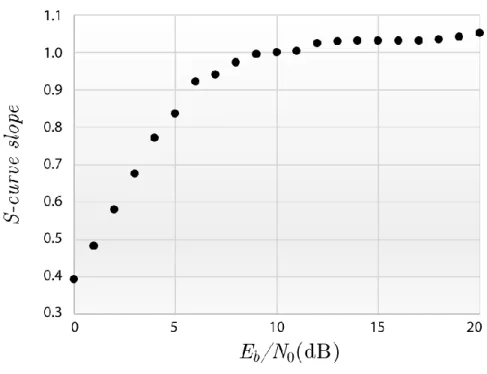
In this work, similarly to what is found in the literature for phase recovery loops with GMSK signals [9], it can be seen that the S-curve changes its shape according to the 𝐸𝑏/𝑁0 ratio. It is shown,
Braz. J. of Develop.,Curitiba, v. 6, n. 10, p. 79016-79040, oct. 2020. ISSN 2525-8761
been numerically obtained through computational simulation in the conditions where the power of the input GMSK signal is 0.5 W and the parameter 𝑔 of the loop is adjusted to 0.7304. From Figure 8 it is observed that the slope of 𝑆(𝜙) is unitary for 𝐸𝑏/𝑁0 = 10 dB.
Figure 8. Slope of 𝑆(𝜙), 𝑎𝑟𝑜𝑢𝑛𝑑 𝜙 = 0, with respect to 𝐸𝑏/𝑁0.
2.6 DESIGN OF THE COSTAS LOOP
This Costas loop may be approximated by a discrete second-order linear system whose system function is [19, 25] 𝐻(𝑧) =𝜃̂[𝑘] 𝜃[𝑘]= (𝑔1+ 𝑔2)𝑧 − 𝑔1 𝑧2− (𝑔 1+ 𝑔2− 2)𝑧 + (1 − 𝑔1) , (31)
where 𝑔1 and 𝑔2, as indicated in Figure 5, are the gains associated to the loop filter. These parameters define the natural frequency 𝜔𝑛, the dumping factor 𝜁 of the equivalent analog system and also the noise bandwidth (𝐵𝐿) of the loop.
Adopting the settling time 𝑡𝑠 = 1 𝑚𝑠 and 𝜁 = 0.707, using the following approximation [26]:
𝑡𝑠 ≅ 4
𝑤𝑛𝜁, (32)
we may determine 𝜔𝑛 = 5,658. The values calculated for 𝜁 and 𝜔𝑛 are employed to determine 𝑔1 and
Braz. J. of Develop.,Curitiba, v. 6, n. 10, p. 79016-79040, oct. 2020. ISSN 2525-8761 𝑔1 = 1 − 𝑒2𝜁𝑤𝑛𝑇𝑠, (33)
𝑔2 = 1 + 𝑒2𝜁𝑤𝑛𝑇𝑠− 𝑒2𝜁𝑤𝑛𝑇𝑠cos (𝑤
𝑛𝑇𝑠√1 − 𝜁2), (33)
that result in 𝑔1 = 1.9995𝑥10−4 and 𝑔2 = 1.9993𝑥10−8.
The noise bandwidth (𝐵𝐿) of the loop is given by [25]:
2𝐵𝐿𝑇𝑠 =
1
2𝜋𝑗∮ 𝐻(𝑧)𝐻(𝑧
−1)𝑧−1𝑑𝑧, (34)
in which the contour integral is defined by |𝑧| = 1 and is oriented counter-clockwise. For 𝐻(𝑧) defined by Eqn (31), we have [25] 2𝐵𝐿𝑇𝑠 = (𝑏1 2 + 𝑏22)(1 + 𝑎2) − 2𝑏1𝑏2𝑎1 (1 − 𝑎2)[(1 + 𝑎2)2− 𝑎 12] , (35)
where 𝑎1 = −(𝑔1+ 𝑔2− 2) , 𝑎2 = (1 − 𝑔1) , 𝑏1 = (𝑔1+ 𝑔2) and 𝑏2 = −𝑔1. Doing the numeric replacements in Eqn (35), we should obtain 2𝐵𝐿𝑇𝑠 = 1.5x10⁻⁴.
In the circumstances where the Gaussian noise is not negligible, the error signal of the loop 𝑒[𝑛] may be modeled as [19]
𝑒[𝑛] = 𝑆(𝜙) + 𝑍[𝑛], (36)
in which 𝑍[𝑛] = 𝑍𝑆[𝑛] + 𝑍𝐺[𝑛], 𝑍𝑆[𝑛] is a portion of noise due to the symbols themselves (self-noise) and 𝑍𝐺[𝑛] the portion derived from the Gaussian noise.
The variance of the phase error of the loop 𝜙[𝑛] = {𝜃 − 𝜃̂[𝑛]} can be determined by the following equation [19]:
𝜎𝜙2 = 2𝐵𝐿𝑇𝑠𝑆𝑧(0), (37)
where 𝑆𝑍(0) corresponds to the power spectral density of the process 𝑍[𝑛] for the frequency 𝑤 = 0. In fact, the Eqn (37) is an approximation to 𝜎𝜙2 that is accurate only if 𝑆𝑍(𝑤) is constant and equal to
𝑆𝑍(0) for |𝑤| ≤ 𝐵𝐿.
The spectral density 𝑆𝑍(0), defined by EQN (37), was numerically determined for differente values of 𝐸𝑏/𝑁0, and the results are presented in figure 9. Only as a reference, using the information in Fig.9 and taking 𝐸𝑏/𝑁0 = 10 dB,, it is found σ_ϕ^2=1.13x10^(-4)rad2. Figure 9. Power spectral
Braz. J. of Develop.,Curitiba, v. 6, n. 10, p. 79016-79040, oct. 2020. ISSN 2525-8761 2.6 SYMBOL SYNCHRONIZER
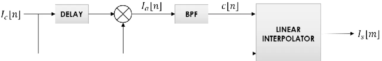
This module receives the baseband signals 𝐼𝑐[𝑛] and 𝑄𝑐[𝑛] from the phase synchronizer and, after processing them, delivers to the symbol detector one sample, for each interval that corresponds to 2𝑇 (8 samples), containing the information associated to the transmitted non-coded symbols 𝑑[2𝑘] and 𝑑[2𝑘 + 1]. The symbol synchronizer, for each 8-sample set of 𝐼𝑐[𝑛] and 𝑄𝑐[𝑛], corresponding to
𝑑[2𝑘] and 𝑑[2𝑘 + 1], respectively, determines the instant of the sample with major signal-to-noise ratio (SNR) on the corresponding analog signal and, through interpolation of the received discrete signal, generates this best sample.
The block diagram of the synchronizer for the signal 𝐼𝑐[𝑛] is shown in Figure 10. An identical scheme is used to recover the synchronization of 𝑄𝑐[𝑛]. The adopted solution is a discrete version of the delay-line multiplier synchronizer [10, 11]. The delay-and-multiply non-linearity (NL) applied to 𝐼𝑐[𝑛] raises a spectral component at frequency 𝑤𝑐 corresponding to the analog frequency of 1/2𝑇 in
𝐼𝑎[𝑛]. The bandpass filter (BPF), centered at 𝑤𝑐, with bandwidth 𝐵𝑐 = 𝑤𝑐/500, filters out 𝐼𝑎[𝑛] and delivers a sinusoidal signal 𝑐[𝑛] at the same frequency and phase of the spectral component produced by NL. Finally, as indicated in Fig. 10, the interpolator receives 𝐼𝑐[𝑛] and 𝑐[𝑛], determines through
interpolation the corresponding value of the sample with major SNR, and delivers it to the symbol detector module in the form of the signal 𝐼𝑠[𝑚] at an 8-times smaller sampling rate.
Braz. J. of Develop.,Curitiba, v. 6, n. 10, p. 79016-79040, oct. 2020. ISSN 2525-8761
Figure 10. Block diagram of the symbol synchronize
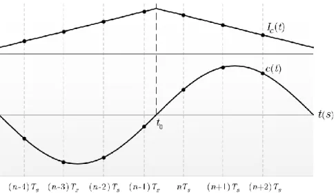
In Figure 11, both analog signals 𝐼𝑐(𝑡) and 𝑐(𝑡), that correspond to the dicrete signals 𝐼𝑐[𝑛] and 𝑐[𝑛], are represented with indications of the sample amplitudes at the instants (𝑛 − 4)𝑇𝑠 through
(𝑛 + 2)𝑇𝑠. From Figure 11, it is evident that the amplitude of 𝐼𝑐(𝑡) is maximized at an instant of time
between (𝑛 − 1)𝑇𝑠 and 𝑛𝑇𝑠. Such instant coincides with time 𝑡0 where 𝑐(𝑡0) = 0 and there is a change in the amplitude of 𝑐(𝑡) from a negative value to a positive one. In this hypothetical scenario, described by Figure 11, it is clear that the samples from 𝐼𝑐(𝑡) have not been taken at the best instant, that is 𝑡0. The interpolator, for every received symbol, performs a linear interpolation to determine the sample that corresponds to the instant 𝑡0 through the following equation:
𝐼𝑠[𝑚] = |𝑐[𝑛 − 1]|𝐼𝑐[𝑛] + |𝑐[𝑛]|𝐼𝑐[𝑛 − 1]
|𝑐[𝑛 − 1]| + |𝑐[𝑛]| , (38)
in which 𝑛 = 8𝑚, i.e., there is a decimation by a factor of 8 to obtain 𝐼𝑠[𝑚]. 𝑄𝑠[𝑚] is derived from 𝑄𝑐[𝑛] following a process identical to the previously mentioned.
The performance of this synchronizer, regarding the variance of the estimated delay, has only been evaluated through computational simulations. The outcomes are exposed and discussed in the next section. An analytical determination of the performance of the synchronizer is currently under investigation.
Braz. J. of Develop.,Curitiba, v. 6, n. 10, p. 79016-79040, oct. 2020. ISSN 2525-8761
3 FS YMBOL DETE CTOR
Figure 11. Relation between the samples of the analog signals Ic(t) and c(t).
The block diagram of the symbol detector module is represented in Figure 12. The signals 𝐼𝑠[𝑚] and 𝑄𝑠[𝑚] are equalized with Wiener filters to reduce ISI, as recommended in [4, 5]. The system
function of the equalizers is
𝑊(𝑧) = 𝑤0+ 𝑤1𝑧−1+ 𝑤2𝑧−2, (39)
where 𝑤0 = 𝑤2 = −0.0859984 and 𝑤1 = 1.0116342.
Figure 12. Block diagram of the symbol detector.
The equalized signals 𝐼𝑒[𝑚] and 𝑄𝑒[𝑚] pass through limiters to obtain the estimates of the
transmitted symbols, denoted by 𝑑̂[2𝑘] and 𝑑̂[2𝑘 + 1], with a sampling rate of 1/2𝑇 to compose the output signal 𝑑̂[𝑘], with sampling rate 1/𝑇, which constitutes the estimate of the non-coded symbol stream that has been transmitted.
Braz. J. of Develop.,Curitiba, v. 6, n. 10, p. 79016-79040, oct. 2020. ISSN 2525-8761
3 NUMERICAL RESULTS AND DISCUSSION
In this section, some results, obtained from computational simulation, about the performance of the proposed GMSK demodulator are presented. Basically, it was determined a curve for the variance of the phase estimated by the Costas loop; a curve for the variance of the symbol delay estimated by the symbol synchronizer; and some curves for the bit error rate of the whole system, where all curves have been built having the energy per bit by the noise power density ratio (𝐸𝑏/𝑁0) as the independent variable.
It is summarized, as follows, the values for the main parameters used in simulation: Carrier Frequency 𝑓𝐼𝐹: 70 MHz;
Symbol Rate 1/𝑇: 10 Mbps; Sampling Frequency 𝑓𝑠: 40 MHz;
Energy per Bit to Noise Power Density 𝐸𝑏/𝑁0: 0 dB through 20 dB; Phase Offset: 0-2𝜋;
Symbol Delay: 0-𝑇;
Frequency Offset: 0-200 kHz.
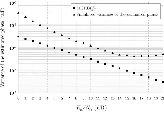
The variance of the phase error with respect to 𝐸𝑏/𝑁0 is shown in Figure 13. It is also depicted, as a reference, the modified Cramer-Rao bound of the phase estimate for GMSK signals, as expressed in the following equation [19]:
MCRB(𝜙) = 𝐵𝐿𝑇
𝐸𝑏/𝑁0. (40)
It can be seen that the curve for the phase error variance lies above the MCRB(𝜙), indicating 𝜎𝜙2 > MCRB(𝜙) for every 𝐸𝑏/𝑁0 value. We can also verify that the simulated variance values agree with the values of 𝜎𝜙2, when determined by Eqn (37), for 𝐸𝑏/𝑁0 ≤ 10 dB and are quite different, if
𝐸𝑏/𝑁0 is near 20 dB.
The discrepancy between the modified Cramer-Rao bound and 𝜎𝜙2, shown in Figure 13, can be explained by the portion of self-noise in the process 𝑍[𝑛], as defined in Eqn (36).
From the results in Figure 13, it is seen that, even with the self-noise contribution, the phase error variance achieves 𝜎𝜙2 ≅ 1.23𝑥10−4rad2, considering 𝐸
𝑏/𝑁0 = 10 dB. Such variance represents
a negligible degradation on the performance of the system.
The modified Cramer-Rao bound of the error in the estimate of the symbol timing for GMSK modulation is given by [19]
Braz. J. of Develop.,Curitiba, v. 6, n. 10, p. 79016-79040, oct. 2020. ISSN 2525-8761 1 𝑇2× MCRB(𝜏) = 1 8𝜋2𝜉𝐿 0 1 𝐸𝑏/𝑁0 , (41) where 𝐿0 is the number of bits in the observation interval and 𝜉 is expressed by [19]
𝜉 = 𝑇 ∫ ℎ2(𝑡)𝑑𝑡, (42)
∞ −∞
In which ℎ(𝑡) is the frequency pulse of the GMSK modulation.
Figure 13. Variance curve for the phase error of the costas loop.
Figure 14 shows the variance curve of the error in the estimate of the symbol delay, resulted from simulation, compared to the Cramer-Rao bound. In this case, 𝐿0 from Eqn (41) is approximated
by
𝐿0 ≅
2𝜋
𝑇𝐵𝑐𝑓𝑠 = 1000,
where 𝐵𝑐 is the bandwidth of the bandpass filter of the symbol synchronizer, as defined in subsection 2.6.
As shown in the graphics of Fig. 14, the error variance for 𝐸𝑏/𝑁0 = 10 dB is approximately 10-14s². Such imprecision on the symbol synchronization results in a negligible loss on the overall system performance.
Braz. J. of Develop.,Curitiba, v. 6, n. 10, p. 79016-79040, oct. 2020. ISSN 2525-8761
Figure 15 depicts the bit error rate (BER) of the demodulator, determined through simulation, under the following conditions: a) with no phase or frequency offset, nor symbol delay; b) with a frequency offset of 200 kHz and a symbol delay of T/2. It is also shown, as a reference, a theoretic curve of a coherent BPSK system with optimal detection.
Figure 14. Variance curve for the error of the estimated symbol delay.
The results from Figure 15 demonstrate that the BER of the proposed architecture is less than 0.5 dB below the theoretical BPSK system performance, for the condition of BER=10-5, even in the
Braz. J. of Develop.,Curitiba, v. 6, n. 10, p. 79016-79040, oct. 2020. ISSN 2525-8761
Figure 15. BER curve of the GMSK demodulator.
4 CONCLUSION
In this paper, it is presented the design of a coherent GMSK demodulator with fully digital architecture, aimed at a high speed (10 Mbps) space telemetry link with large Doppler offset. All functional modules of the demodulator were detailed through block diagrams and equations. Some original and unprecedented mathematical analysis were developed to better explain the functionalities of the modules, notably for the Costas loop employed in the phase recovery.
The results from computational simulations indicate that the adopted solutions for the carrier and symbol synchronizers are certainly effective, and that there is no practical impact on the 𝐸𝑏/𝑁0 ratio of the demodulator even in the existence of a large carrier frequency offset and a significant symbol delay. Furthermore, it became clear that there is no loss of any transmitted symbol due to the synchronization process in the proposed architecture.
The performance of the proposed demodulator, concerning the bit error rate, reveals a small loss of less than 0.5 dB when compared to an optimal BPSK demodulator for the condition where BER = 10-5. It is noteworthy that the performance of the system is remarkably satisfactory, considering the
Braz. J. of Develop.,Curitiba, v. 6, n. 10, p. 79016-79040, oct. 2020. ISSN 2525-8761
ACKNOWLEDGEMENT
This work was supported by the Brazilian Space Agency (AEB) and the National Council for Scientific and Technological Development (CNPq) through Edital MCT/CNPq/AEB nº 33/2010.
REFERENCES
[1] MUROTA, Kazuaki; HIRADE, Kenkichi. GMSK modulation for digital mobile radio telephony. IEEE Transactions on communications, v. 29, n. 7, p. 1044-1050, 1981.
[2] SIMON,MARVIN K.BANDWIDTH-EFFICIENT DIGITAL MODULATION WITH APPLICATION TO DEEP -SPACE COMMUNICATIONS.JOHN WILEY &SONS,2005.
[3] SHAMBAYATI, Shervin; LEE, Dennis K. GMSK modulation for deep space applications. In:
Aerospace Conference, 2012 IEEE. p. 1-13., 2012.
[4] CCSDS Recommendations for Space Data System Standards. Bandwidth-efficient modulations, CCSDS 413.0-G-1, Green Book, CCSDS, Apr. 2003.
[5] SESSLER, G. M.; ABELLO, R.; JAMES, N.; MADDE, R.; VASSALLO, E. GMSK demodulator implementation for ESA deep-space missions. Proceedings of the IEEE, v. 95, n. 11, p. 2132-2141, 2007.
[6] RAMAMURTHY, Arjun et al. An All Digital Implementation of Constant Envelope: Bandwidth Efficient GMSK Modem using Advanced Digital Signal Processing Techniques. Wireless
personal communications, v. 52, n. 1, p. 133, 2010.
[7] SHAH, Santosh; SINHA, V. GMSK demodulator using costas loop for software-defined radio. In: Advanced Computer Control, 2009. ICACC'09. International Conference on. IEEE, p. 757-761., 2009.
[8] SILVA, A. S.; LUCENA, A. M. P.; MOTA, J. C. M. Demodulador OQPSK: Implementação Completamente Digital para Aplicações Espaciais. Novas Edições Acadêmicas, 2014.
[9] VASSALLO, Enrico; VISINTIN, Monica. Carrier phase synchronization for GMSK signals.
International Journal of Satellite Communications and Networking, v. 20, n. 6, p. 391-415, 2002.
[10] IMBEAUX, J.-C. Performances of the delay-line multiplier circuit for clock and carrier synchronization in digital satellite communications. IEEE Journal on Selected Areas in
Communications, v. 1, n. 1, p. 82-95, 1983.
[11] D'ANDREA, A.; MENGALI, U. Performance analysis of the delay-line clock regenerator.
IEEE transactions on Communications, v. 34, n. 4, p. 321-328, 1986.
[12] KALEH, G. Simple coherent receivers for partial response continuous phase modulation. IEEE
Journal on Selected Areas in Communications, v. 7, n. 9, p. 1427-1436, 1989.
[13] LAURENT, P. Exact and approximate construction of digital phase modulations by superposition of amplitude modulated pulses (AMP). IEEE transactions on communications, v. 34, n. 2, p. 150-160, 1986.
[14] LUCENA, A. M. P. et al. Fully digital BPSK demodulator for satellite supressed carrier telecommand system. International Journal of Satellite Communications and Networking, v. 35, n. 4, p. 359-374, 2017.
[15] PROAKIS, J. G.; SALEHI, M. Digital communications. 5. ed. McGraw-Hill, 2008.
[16] CCSDS Recommendations for space data system standards. Radio Frequency and Modulation Systems -PART 1: Earth stations and Spacecraft, CCSDS 401.0-b-1tc1. BLUE BOOK, July 2011. [17] MORELLI, M.; MENGALI, U. Feedforward carrier frequency estimation with MSK-type signals. IEEE Communications Letters, v. 2, n. 8, p. 235-237, 1998
Braz. J. of Develop.,Curitiba, v. 6, n. 10, p. 79016-79040, oct. 2020. ISSN 2525-8761
[18] PENG, Hua; LI, Jing; GE, Lindong. Non-data-aided carrier frequency offset estimation of GMSK signals in burst mode transmission. In: Acoustics, Speech, and Signal Processing, 2003.
Proceedings.(ICASSP'03). 2003 IEEE International Conference on. IEEE, p. IV-576. ,2003.
[19] MENGALI, Umberto. Synchronization techniques for digital receivers. Springer Science & Business Media, 2013.
[20] JHAIDRI, Mohamed Amine; LAOT, Christophe; THOMAS, Alain. Nonlinear analysis of GMSK carrier phase recovery loop. In: Signal, Image, Video and Communications (ISIVC),
International Symposium on. IEEE, p. 230-235., 2016.
[21] TYTGAT, M.; STEYAERT, M.; TEYNAER, P. Time domain model for costas loop based QPSK receiver. In: Ph. D. Research in Microelectronics and Electronics (PRIME), 2012 8th
Conference on. VDE, 2012.
[22] RAGHVENDRA, M. R. et al. Design and development of high bit rate QPSK demodulator. In:
Electronics, Computing and Communication Technologies (CONECCT), 2013 IEEE International Conference on. IEEE, 2013.
[23] KUZNETSOV, N. V. et al. Simulation of nonlinear models of QPSK Costas loop in Matlab Simulink. In: Ultra Modern Telecommunications and Control Systems and Workshops (ICUMT), 2014
6th International Congress on. IEEE, 2014.
[24] PACELLI, R. V; LUCENA, A. M. P.; FIGUEIREDO, S. S. Técnica de sincronização de portadora para sistemas de comunicação OFDM. Brazilian Journal of Development 6.3 (2020): 14297-14305. [25] LINDSEY, W. C.; CHIE, C. M. A survey of digital phase-locked loops. Proceedings of the
IEEE, v. 69, n. 4, p. 410-431, 1981.
[26] GARDNER, Floyd M. Phaselock techniques. John Wiley & Sons, 2005.
[27] LI, W.; MEINERS, J. Introduction to phase-locked loop system modeling. Analog Applications (2000).
![Figure 6. discrete pulse shape at the output of the c 0 [n] filter.](https://thumb-eu.123doks.com/thumbv2/123dok_br/17631103.821403/10.893.190.701.453.587/figure-discrete-pulse-shape-output-c-n-filter.webp)