Telmo Filipe Pereira Ferraria
Verification of Analog Circuits in Power-Down
Mode
Dissertação para obtenção do Grau de Mestre em Engenharia Eletrotécnica e Computadores
Orientadora :
Maria Helena Fino, Doutora, Faculdade de
Ciên-cias e Tecnologia da Universidade Nova de
Lis-boa
Co-orientador :
Helmut Gräeb, Doutor, Technische Universität
München
Júri:
Presidente: Fernando José Vieira do Coito
Arguentes: João Pedro Oliveira
iii
Verification of Analog Circuits in Power-Down Mode
Copyright cTelmo Filipe Pereira Ferraria, Faculdade de Ciências e Tecnologia, Univer-sidade Nova de Lisboa
Acknowledgements
Este espaço é dedicado a todos aqueles que me acompanharam durante o percurso académico na FCT e na TUM-EDA. Para todos eles, o meu mais sincero obrigado!
Agradeço á Professora Doutora Maria Helena Fino a amizade orientação e apoio con-stante ao longo de todo o meu percurso académico assim como na minha dissertação. Gostaria também de lhe agradecer a oportunidade de ter realizado a minha dissertação em Munique, com esta eu cresci muito como pessoa.
I would like to thank to Dipl. Eng. Michael Zwerger and Prof. Dr. Eng. Helmut Gräeb for providing an excellent working environment and for all the technical support and advice that made this work possible all the time that I have been in the TUM-EDA.
Ao Departamento de Engenharia Eletrotécnica da Universidade Nova de Lisboa pelo uso das instalações e por ter sido ao longo destes anos uma segunda casa.
Gostaria também de agradecer aos meus colegas de casa Miguel Duarte, Pedro Car-taxo e Sérgio Pinto por todo o tempo que passamos juntos. Aos colegas Fábio Passos, Rui Lopes, Marisa Amaral e a Filipa Lourenço porque foram a minha segunda família durante estes anos.
Ao Pedro Leitão todos os momentos que passamos desde pequenos como jogadores de hóquei até aos últimos três meses em Munique.
Para os colegas Hugo Viana e José Vieira não tenho palavras para descrever o que passei com eles durante o meu percurso académico. Agradeço todo o apoio e força que me transmitiram sempre nas alturas mais complicadas. Todos os bons momentos passa-dos.
viii
com a minha família em particular com os meus pais e irmã, por todo o apoio e carinho que me deram ao longo da minha vida e que sem eles seria impossível alcançar esta meta.
Abstract
The energy efficiency and optimization are two important points of analog circuits. With purpose to reduce the power consumption, most of these circuits are equipped with power-down features, which means the circuits are idle when they are not used. In power-down mode internal nodes can have floating states which results in an increase of the transistor degradation.
In this thesis a computer program that checks the node voltage levels and the state of the transistors in power-down mode is presented. The search procedure will ensure that all currents in the paths are safely turned off. The program works just with the structural information of the circuit given into a input file i.e net-list file. No numerical simulation is needed.
Resumo
A maximização energética bem como otimização nos circuitos analógicos é uma pre-ocupação fundamental na concepção de circuitos analógicos. De forma a reduzir o seu consumo muitos circuitos incluem sistemas deP ower−Downque diminuem a corrente quando o mesmo não é necessário. Contudo ao se encontrar em modoP ower−Down
algumas das tensões internas podem ter um valor indefinido o que por sua vez se traduz num aumento na degradação dos transístores até a sua falha.
Nesta dissertação um programa que estima corretamente os níveis de tensão e os estados dos transístores quando o circuito se encontra em modoP ower−Downé apre-sentado. O mesmo garante que não existe corrente a fluir nos circuitos em modoP ower−
Down.
Para o funcionamento do programa apenas um ficheiro contendo o esquemático do circuito sem dimensões é necessário.
Contents
1 Introduction 1
1.1 Motivation . . . 1
1.2 Goals of the Work . . . 2
1.3 State of the Art . . . 2
1.4 Outline of the Thesis . . . 3
2 Voltage Propagation in Power-Down 5 2.1 Problem Formulation . . . 5
2.2 Voltage Propagation in elementary blocks . . . 6
2.3 Summary . . . 12
3 Verification Tool for Circuits in Power-Down Mode 13 3.1 Voltage Propagation Analysis . . . 14
3.1.1 Mapping of Circuit Components into Graph Branches . . . 15
3.1.2 State Mapping . . . 18
3.1.3 Voltage Propagation Algorithm . . . 21
3.1.4 Working Example . . . 22
3.2 Short Circuit Analysis . . . 24
3.2.1 Depth-First Search Algorithm . . . 26
3.2.2 Fix and Reset . . . 28
3.2.3 Short Circuit Algorithm . . . 30
3.3 Stress Analysis . . . 31
3.3.1 Stress Algorithm . . . 33
3.4 All Program . . . 34
3.5 Summary . . . 35
4 Results 37 4.1 Two-stage Amplifier . . . 38
xiv CONTENTS
4.3 Industrial Circuit . . . 48 4.4 Integration with Cadence Software . . . 51 4.5 Summary . . . 53
List of Figures
2.1 Differential Stage With Power-Down Switch [ZG12] . . . 6
2.2 Propagation of Positive Charge in Resistor . . . 7
2.3 Propagation of Negative Charge in Resistor . . . 7
2.4 Propagation of Positive Charge in Capacitor . . . 8
2.5 Propagation of Negative Charge in Capacitor . . . 8
2.6 Propagation of Positive Charge in Diode . . . 9
2.7 Propagation of Negative Charge in Diode . . . 9
2.8 Transistor in Diode Configuration . . . 10
2.9 Transistor in General Configuration . . . 10
2.10 Propagation in Transistor with Gate Connected toNvdd . . . 10
2.11 Propagation in Transistor with Gate Connected toNvss . . . 11
2.12 Propagation in Transistor with Gate floating . . . 11
3.1 Block Diagram of an Automatic Voltage Propagation Analysis . . . 14
3.2 Liberal State Mapping for CMOS Transistors . . . 19
3.3 Conservative differences . . . 19
3.4 Pseudo-Code for Voltage Propagation Algorithm . . . 21
3.5 Propagation ofvddvoltage level . . . 21
3.6 Propagation ofvssvoltage level . . . 21
3.7 Example of Voltage Propagation Analysis . . . 22
3.8 Block Diagram of Short Circuit Analysis . . . 24
3.9 Example of Short-Circuit Path and Potential Short Circuit Path . . . 25
3.10 Depth-First Search . . . 26
3.11 Pseudo-Code forDepth−F irst Searchalgorithm . . . 26
3.12 Pseudo-Code forGo-T o N ext N odeFunction . . . 27
3.13 Pseudo-Code forCheck Connectionsfunction . . . 28
3.14 Resetting and Fixing . . . 28
xvi LIST OF FIGURES
3.16 Block Diagram of Stress Analysis . . . 31
3.17 Remove Power-down Switches . . . 31
3.18 Example of Stress Analysis . . . 33
3.19 Pseudo-Code forStressalgorithm . . . 33
3.20 Bock Diagram of Verification of Power-Down Mode Program . . . 34
4.1 Two-Stage Amplifier Schematic . . . 38
4.2 Graph Representation of Two-Stage Amplifier before Voltage Propagation Analysis . . . 39
4.3 Graph Representation of Two-Stage Amplifier after Voltage Propagation Analysis . . . 40
4.4 Graph Representation of Two-Stage Amplifier after Short Circuit Analysis 41 4.5 Two-Stage Amplifier with Verification Tool . . . 42
4.6 BiCMOS Circuit With One Power-Down Switch . . . 44
4.7 Graph Representation of BiCMOS Circuit with One Power-Down Switch After Verification Tool . . . 45
4.8 BiCMOS Circuit With Two Power-Down Switches . . . 46
4.9 Graph Representation of BiCMOS Circuit with Two Power-Down Switches After Verification Tool . . . 47
4.10 OTA Circuit . . . 49
4.11 Differences in Industrial Circuit . . . 50
4.12 Two Stage Amplifier in Cadence With Verification Tool and Interface . . . 51
4.13 Defined States in Cadence . . . 52
List of Tables
3.1 Mapping of Two Terminal Devices . . . 15
3.2 Mapping of Transistor Component Devices . . . 17
3.3 Node Voltage Levels . . . 18
3.4 Conservative State Mapping for CMOS Transistors . . . 20
3.5 Conservative State Mapping . . . 20
3.6 Structure Rules File . . . 32
4.1 Nodes expected withvssandvddVoltage Level of Two-Stage Amplifier . . 42
4.2 Expected State of Transistors of Two Stage Amplifier . . . 43
4.3 Current Consumption (DC) . . . 44
4.4 Expected Voltage Levels in BiCMOS Circuit . . . 47
4.5 Nodes with ExpectedvddVoltage Level in Industrial Circuit . . . 48
4.6 Nodes with ExpectedvssVoltage Level in Industrial Circuit . . . 48
1
Introduction
1.1
Motivation
Reliability in CMOS is one of the biggest problems for the analog circuits in the world. Reliability, is defined as the probability of a product operating for a given amount of time under specified conditions without failure [Ohr98]. Reliability is highly affected by circuit aging, i.e, the deterioration of the circuit’s performance over its lifetime. The lifetime can vary from a few years to a few months under worst-case scenarios.
Circuit deterioration may lead to power consumption increase and in extreme cases, circuit aging may even cause functional failures to occur.
The introduction of new materials in CMOS technologies raised additional mecha-nisms that may become faulty or generate system failures. Hot carrier injection (HCI) and bias temperature instability (BTI) are two push mechanisms responsible for the degrada-tion of transistors and consequently of an integrated circuit [MG11],
[CMFSL11].
These modifications resulted in a change of CMOS transistors characteristics, such as the threshold voltage, decrease in drain current and transconductance [SBA+
03].
Furthermore circuit aging is particularly affected by mismatching. A mismatch may occur due to either process variations or stress-induced degradation during the device operation, such as when large asymmetrical voltages are applied to the transistors [CZT+
01], [MG11].
Experimental studies have shown that mismatches in differential amplifiers and cur-rent mirrors are reinforced by HCI degradation, which in turn contributes to the degra-dation of the circuits performance over time [PG11].
1. INTRODUCTION 1.2. Goals of the Work
designers. In order to save battery power and to reduce the chip heat most of the analog circuits are equipped with power-down features, which means the circuit will be idle when not in use.
During power-down mode, the potentials of the internal nodes is determined by the sub-threshold characteristics of the devices, leakage paths and by the signals applied to the inputs [SBA+
03].
This nodes can cause asymmetrical stress conditions in structures.
1.2
Goals of the Work
While it is relatively easy to check small circuits manually, larger circuits often have many pitfalls that could be easily missed. The overall goal of this Thesis is to develop a computer program capable of analyzing large circuits, with the ability to estimate node voltage levels and the state of transistors in power-down mode, based on the circuit struc-ture.
This program detects if there is current flowing in paths when the circuit is in power-down mode. A fully automatic checking system of stress-sensitive structures was pro-posed as a future work [ZG12]. Therefore the program implements this automatic detec-tion.
Furthermore, in order to help the circuit-designer, the program is integrated into CA-DENCE Software.
1.3
State of the Art
Since the problem addressed is relatively new, very few work has been developed in this area. This section presents the relevant research concerning the development of algorithms to use in analog circuits in power-down mode. The first algorithm was pro-posed by [BJ96]. They developed two versions of the voltage propagation algorithm, one considered a basic version and another one considered to be a more elaborated version.
These algorithms take under consideration two linked lists which contain all compo-nents and all nodes of the circuit. In the basic version three voltage levels are considered, gndlevel which is equal to the lowest voltage,vddwhich is equal to the positive supply voltage orfloatwhen the voltage is unknown or the node has high impedance. The ba-sic version is limited to resistors and MOS devices, the possibility of current being put into forward biased junctions is not considered and diodes components are equally not considered.
In the elaborated version, the limitations of the basic version are overcome by extend-ing the number of the possible voltage levels of a node to six. In this version they consider gnd,vdd,float,curr,pullupandpulldownvoltage levels.
1. INTRODUCTION 1.4. Outline of the Thesis
voltage level is used when current is detected in a component. Yet, even with this defini-tion the node voltage levels are not correctly estimated.
Recently a new version of the voltage propagation algorithm was proposed [ZG12]. Although it is based on the same principles as the ones used by [BJ96], this version in-cludes MOS and bipolar transistors, resistor, capacitor and diodes.
Furthermore, some transistor configurations are considered, such diode configura-tion. The circuit is transformed into a directed graphical representation, containing all connections and nodes of the circuit.
The proposed algorithm indicates if the node voltages are correctly estimated and floating nodes are detected.
Both versions of voltage propagation algorithm rely on the representation of the cir-cuit from an input file which contains the net-list of the circir-cuit. No electrical simulation or aging simulation is needed. Therefore, algorithms that identify the types of components and nodes existing in the net list file are needed [MGS08].
These algorithms involve a creation of an hierarchical library which contains basic CMOS and bipolar build blocks, like e.g., transistors, current mirrors and a differential stage. Then the algorithm identifies the presence of these elements in the given circuit net-list.
1.4
Outline of the Thesis
2
Voltage Propagation in Power-Down
In this chapter an introduction to the voltage propagation behaviour in circuits in power-down mode is presented.
Firstly, a brief formulation of the problem is introduced in section 2.1.
Then, to detect the problems described in section 2.1, each elementary circuit com-ponent was tested. These tests are described section 2.2 where a theoretical prevision is presented and the corresponding transient analysis is performed to validate the assump-tions made.
2.1
Problem Formulation
The problems of analog circuits in power-down mode are illustrated with the differ-ential stage represented in figure 2.1.
Here, transistorM1 is a power-down switch, so in order to put the circuit in the idle
mode it is necessary to turn the current inM2 off by connecting thenpwd to a negative
supply voltage. As a result of this,nbiaswill be pulled up tovdd. SinceM2 is off there is
no tail current, consequently no current flows through inM3 orM4. The voltages ofn1
andn3 nodes depend on the sub-threshold characteristics of the devices, leakage paths
and by the signals applied to the inputs. As these voltage levels cannot be defined asvss orvddit is considered that nodesn1andn3are floating.
In power-down mode, if the gate of a transistor is floating, it is impossible to define in which state it’s in. Thus, potential current flow in the paths that contain these transistors. In matched structures this kind of node will cause asymmetrical stress conditions.
2. VOLTAGEPROPAGATION INPOWER-DOWN 2.2. Voltage Propagation in elementary blocks
M3 M4 n1 M1
M2 VDD
M6 n3
M5 n2
VSS npwd
nbias
nin+ nin−
power-down switch
differential pair
Figure 2.1: Differential Stage With Power-Down Switch [ZG12]
methodology for detecting these situations is of great importance. In order to automati-cally identify stress conditions, the voltage propagation along the circuits is addressed in the following subsection.
2.2
Voltage Propagation in elementary blocks
According to previous publication [ZG12], a voltage propagation algorithm can be developed to estimate the node voltages and detect floating nodes in power-down mode. With the purpose of illustrating how the voltage propagation works in circuits, a first analysis of the propagation in the elementary blocks is addressed.
For the voltage propagation to work well it is fundamental to guaranty that the cur-rent is interrupted giving rise to an adjustment of the charges in the circuit.
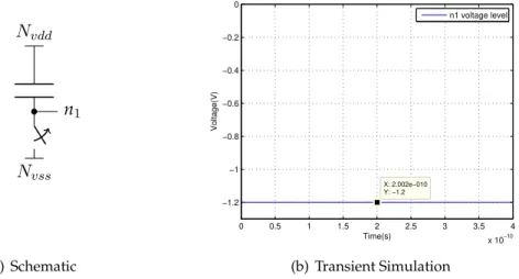
The voltage propagation behaviour in a resistor is shown in Figures 2.2 and 2.3. In Figure 2.2(a), when the switch is open the current becomes zero and the voltage level in
n1will rise to value of positive supply.
2. VOLTAGEPROPAGATION INPOWER-DOWN 2.2. Voltage Propagation in elementary blocks
Nvdd
Nvss
n1
(a) Schematic
0 0.5 1 1.5 2 2.5 3 3.5 4
x 10−10
−1 −0.5 0 0.5
1 X: 2.002e−010Y: 1.2
Time(s)
Voltage(V)
X: 2e−010 Y: −1.2
n1 voltage level
(b) Transient Simulation
Figure 2.2: Propagation of Positive Charge in Resistor
In the circuit represented in Figure 2.3 the voltage value ofn1 becomes equal to the
negative supply.
Nvdd
Nvss
n1
(a) Schematic
0 0.5 1 1.5 2 2.5 3 3.5 4
x 10−10
−1 −0.5 0 0.5
1 X: 1.984e−010Y: 1.2
Time(s)
Voltage(V)
X: 2.002e−010 Y: −1.2
n1 voltage level
(b) Transient Simulation
Figure 2.3: Propagation of Negative Charge in Resistor
Since resistors have no polarity, the propagation method for the other direction is also to be considered.
Figures 2.4 and 2.5 represent the voltage propagation in a capacitor. In this situation the charge in the capacitor remains constant. As resultn1 has the same value when the
2. VOLTAGEPROPAGATION INPOWER-DOWN 2.2. Voltage Propagation in elementary blocks
Nvdd
Nvss
n1
(a) Schematic
0.5 1 1.5 2 2.5 3 3.5 4
x 10−10
0.2 0.4 0.6 0.8 1 1.2 1.4
Time(s)
Voltage(V)
n1 voltage level
(b) Transient Simulation
Figure 2.4: Propagation of Positive Charge in Capacitor
While in Figure 2.4(b) the transient analysis shows that the voltage remains in 1.2 V, in Figure 2.5(b) this value remains in -1.2 V before and after of the switch is open.
Nvdd
Nvss
n1
(a) Schematic
0 0.5 1 1.5 2 2.5 3 3.5 4
x 10−10
−1.2 −1 −0.8 −0.6 −0.4 −0.2 0
X: 2.002e−010 Y: −1.2
Time(s)
Voltage(V)
n1 voltage level
(b) Transient Simulation
Figure 2.5: Propagation of Negative Charge in Capacitor
In the diode component the voltage propagation can occur only in one direction be-cause the diode only conducts current if the anode has a higher voltage than the cathode. The diode represented in Figure 2.6(a) was simulated. The charge will flow across the diode andn1will reach the positive supply value when the switch is open. The transient
2. VOLTAGEPROPAGATION INPOWER-DOWN 2.2. Voltage Propagation in elementary blocks
Nvdd
Nvss
n1
(a) Schematic
0 1 2 3 4 5 6
x 10−4
0.8 0.85 0.9 0.95 1 1.05 1.1 1.15 1.2 1.25 Time(s) Simulation Voltage(V)
n1 voltage level
(b) Transient Simulation
Figure 2.6: Propagation of Positive Charge in Diode
For the case where the diode is connected in the configuration represented in Fig-ure 2.7(a), when the switch is open the charge in n1 will flow across the diode and n1
will reach the value of the negative supply. The transient analysis results represented in Figure 2.7(b) proves the expected result.
Nvdd
Nvss
n1
(a) Schematic
0 1 2 3 4 5 6
x 10−4
−1.2 −1.15 −1.1 −1.05 −1 −0.95 −0.9 −0.85 −0.8 Voltage(V) Time(s) Simulation
n1 voltage level
(b) Transient Simulation
Figure 2.7: Propagation of Negative Charge in Diode
2. VOLTAGEPROPAGATION INPOWER-DOWN 2.2. Voltage Propagation in elementary blocks
n
bn
dgn
sFigure 2.8: Transistor in Diode Configuration
Figure 2.9 shows a transistor in a general configuration. In this case the propagation will depend on the state of the transistor, thus several transistor biasing configuration will be discussed.
n
bn
gn
dn
sFigure 2.9: Transistor in General Configuration
The operation regions will depend on the gate voltage level, so the gate of the tran-sistor will control the voltage propagation.
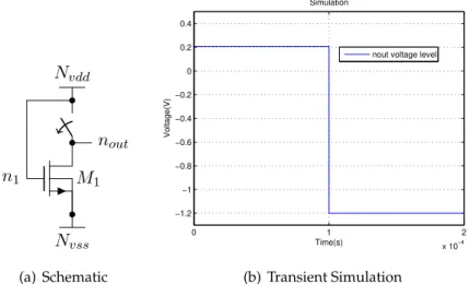
Figure 2.10(a) can be used to explain how the propagation works in circuits with transistors. In power-down mode the current in the path should be zero. Therefore, it is necessary open the switch. If then1node was connected toNvddnode thenM1transistor
can propagate, leading the propagation of the charge onNvsstonout. As resultnoutnode
voltage becomes equals to the negative supply.
M1 Nvdd
n1
nout
Nvss
(a) Schematic
0 1 2
x 10−4
−1.2 −1 −0.8 −0.6 −0.4 −0.2 0 0.2 0.4
Time(s)
Voltage(V)
Simulation
nout voltage level
(b) Transient Simulation
2. VOLTAGEPROPAGATION INPOWER-DOWN 2.2. Voltage Propagation in elementary blocks
The transient analysis represented in Figure 2.10(b) shows thatnoutnode change the
voltage level to -1.2 when the gate ofM1 is connected toNvss.
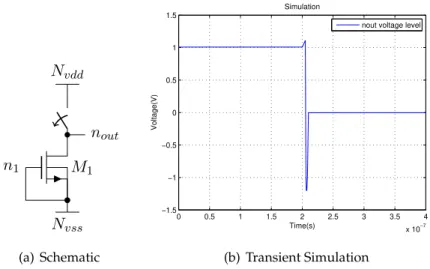
In the second case the circuit in Figure 2.11(a) with then1 node connected toNvss is
considered. As resultM1 transistor cannot propagate andnouthas floating state. In this
situation it’s not possible to define whether the voltage level innoutis equal to a positive
or negative supply and the transient analysis in Figure 2.11(b) can prove it.
M1 Nvdd
n1
nout
Nvss
(a) Schematic
0 0.5 1 1.5 2 2.5 3 3.5 4
x 10−7
−1.5 −1 −0.5 0 0.5 1 1.5
Time(s)
Voltage(V)
Simulation
nout voltage level
(b) Transient Simulation
Figure 2.11: Propagation in Transistor with Gate Connected toNvss
The last case is similar to the previous one, if the gate of M1 is floating, then it’s
impossible to define if the propagation is possible. Thusnouthas again floating state.
M1 Nvdd
n1
nout
Nvss
Figure 2.12: Propagation in Transistor with Gate floating
For the complementary type of transistor the same behavior was obtained.
2. VOLTAGEPROPAGATION INPOWER-DOWN 2.3. Summary
2.3
Summary
Stress conditions in circuits in power-down mode lead to severe aging problems in the circuits. To avoid stress conditions, voltage propagation in circuit must be performed so that such situations may be identified and duly corrected.
3
Verification Tool for Circuits in
Power-Down Mode
The analysis performed regarding the verification of power-down mode program will be described throughout this chapter.
The verification tool starts by applying the voltage propagation behavior described in Chapter 2. The methodology adopted for the automatic evaluation of the voltage propa-gation will be presented in section 3.1. Then, in section 3.2 a short circuit analysis yielding the evaluation of the paths for current flowing is presented.
Section 3.3 relates to a fully automated stress analysis check of stress-sensitive topolo-gies.
3. VERIFICATIONTOOL FORCIRCUITS INPOWER-DOWNMODE 3.1. Voltage Propagation Analysis
3.1
Voltage Propagation Analysis
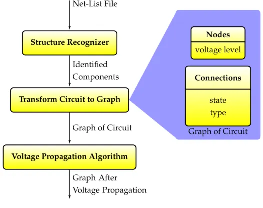
Figure 3.1 shows the several steps performed during the voltage propagation analy-sis.
Firstly theStructure Recognizerblock receives the circuit representation given in the netlist. This block runs the algorithm described in [MGS08], where elementary compo-nents are identified.
Nodes
voltage level
Connections
state type
Structure Recognizer
Transform Circuit to Graph
Voltage Propagation Algorithm
Identified Components
Graph of Circuit
Graph After
Voltage Propagation Net-List File
Graph of Circuit
Figure 3.1: Block Diagram of an Automatic Voltage Propagation Analysis
In theTransform Circuit to Graphblock, a graph representation of the interconnections between the previously identified structures is generated. In this graph, the nodes con-tain information regarding the corresponding voltage level, whereas the branches concon-tain information relative to the type and the state of the connections between the nodes.
The types for connections considered are described in Section 3.1.1. The description of the states for each connection appears in Section 3.1.2 as well as the description of the voltage levels for the nodes.
Then the graph representation is used by theVoltage Propagation Algorithmblock, re-sponsible for the execution of the voltage propagation algorithm described in section 3.1.3. The propagation changes the voltage levels in nodes and the state of the connec-tions in graph representation.
After the analysis has been completed, a graph representation containing an estima-tion of the voltage level in each node and the state of connecestima-tions is obtained.
3. VERIFICATIONTOOL FORCIRCUITS INPOWER-DOWNMODE 3.1. Voltage Propagation Analysis
short circuit and stress analysis.
3.1.1 Mapping of Circuit Components into Graph Branches
According to the type of component, different types of connections are generated. Each connection contains one of the three types identified below.
• diode-type (dio)
• n-switch(nsw)
• p-switch(psw)
In this work, a component mapping for two terminal devices and transistors were in-cluded.
Figure 3.1 shows the two terminal devices considered while the transistors are con-sidered in Figure 3.2.
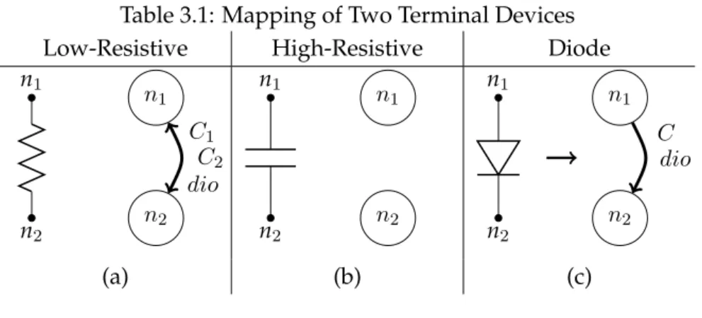
For the two terminal devices three possible types are accounted for:
• Resistor: For this device two branches are generated because the resistor prop-agates the voltage in both directions. The column in Table 3.1 (a) shows these branches (C1 and C2) with bidirectional arrow and the type of them is diode-type
(dioin the Table 3.1 (a)).
• Capacitor: In this case no connection is generated, because no current flows in
either direction.
• Diode: In diode component one branch from anode to cathode is generated. This is represented in Table 3.1 (c). The type of this connection is diodediode-type.
Table 3.1: Mapping of Two Terminal Devices
Low-Resistive High-Resistive Diode
n2
n1
n2 n1
C1 C2 dio
n2
n1
n2 n1
n2
n1
n2 n1
C dio
3. VERIFICATIONTOOL FORCIRCUITS INPOWER-DOWNMODE 3.1. Voltage Propagation Analysis
For bipolar and MOS technologies three possible configurations are considered for the transistors.
• Diode-Connected: For NMOS ornpn, one connection from drain/gate to source or base/collector to emitter is created. For PMOS orpnp one connection from source to drain/gate or from emitter to base/collector is created. In both cases the type of connection isdiode-type. Table 3.2(a) shows a representation of this kind of configu-ration.
• Off-Connected: In this type of configuration the direction of the connections are re-versed to diode-connected. For NMOS ornpnone connection from source/gate to drain or emitter/base to collector is created. For PMOS orpnpone connection from drain to source/gate or from collector to emitter/base is created. In both cases the type of connection isdiode-type, as shown in Table 3.2(b).
• Switch: In switch configuration, two connections are generated. These are
rep-resented by a bidirectional arrow in Table 3.2(c). The type of the connection will depend on the type of transistor, which means if it’s a NMOS ornpn transistor, it will be a n-switchconnection. If it is PMOS or pnp transistor, then it’s ap-switch connection. The dotted arrows in Table 3.2(c) represent the switch relation. As we can observe the switch connections change depending if they are connected to the gate or to the base.
For MOS technology the parasites bulk-drain and bulk-source diode is considered. In this case two graph branches are generated and the direction of these connections depends on whether it’s a NMOS or PMOS. The branches start in bulk when it’s a NMOS transistor and finishes in bulk when it’s a PMOS transistor.
3. VERIFICATIONTOOL FORCIRCUITS INPOWER-DOWNMODE 3.1. Voltage Propagation Analysis
Table 3.2: Mapping of Transistor Component Devices
Diode-connected Off-connected Switch
ncb
ne
nencb
Cce
dio
nc
neb
nebnc
Cec
dio
nb
nc
ne
nenc nb switch relation Cbc dio Cbe dio Cce Cec nsw NPN
ncb
ne
ncb ne Cec dionc
neb
nc neb Cce dionb
nc
ne
nc ne nb switch relation Ceb dio Ccb dio Cec Cce psw PNPnb
ndg
ns
nsndg
nb Cds
dio Cbd dio Cbs dio
nb
nd
nsg
nsgnd
nb Csd
dio Cbd dio Cbs dio
nb
ng
nd
ns
nsnd ng nb Cds Csd nsw Cbd dio Cbs dio relation switch NMOS
nb
ndg
ns
ndg nsnb Csd
dio Csb dio Cdb dio
nb
nd
nsg
ndg nsgnb Cds
dio Csb dio Cdb dio
nb
ng
nd
ns
nd ns ng nb relation switch Csd Cds psw Csb dio Cdb dio PMOS3. VERIFICATIONTOOL FORCIRCUITS INPOWER-DOWNMODE 3.1. Voltage Propagation Analysis
3.1.2 State Mapping
Before the state of connections is defined, it is necessary to appraise the node voltage levels. For each node the following three voltage levels are to be considered:
• vdd: when the estimated value in the node is equal to positive supply voltage.
• vss: when the estimated value in the node is equal to negative supply voltage.
• f loating: when it is impossible estimate the value of node.
In order to ease the comprehension, different colors have been attributed to the dif-ferent voltage levels. Red represents thevddvoltage level. The node that is expected to bevssis yellow and the blue represents thefloatingvoltage level. This is shown in Table 3.3.
Table 3.3: Node Voltage Levels
vdd floating vss
node node node
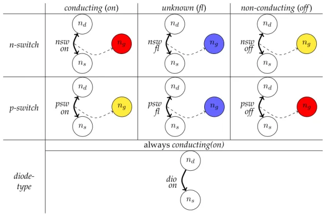
If the type of connection and node voltage levels are known, then it’s possible to ascertain the state of the connection. As previously cited there are three possible states [ZG12].
• conducting: when the state of connection is conducting.
• non-conducting: when the state of connection is not conducting.
• unknown: when it is impossible define the state of connection.
Two versions of state mapping were introduced in voltage propagation analysis. TheLiberalversion as previously published [ZG12] and theConservativeversion, which consists of a new approach. The difference between these two versions resides in the switching relation. InLiberalonly the gate/base voltage level is pondered. In Conserva-tivethe gate/base and source/emitter voltage levels are weighted.
Figure 3.2 shows theLiberalversion, where, fordiode-typeconnections the state is al-ways considered to beconducting.
For switch type connections the state depends on the gate (switch relation) voltage level. The connection is considerednon-conducting, when the type of the connection is n-switchand the gate (switch relation) voltage level isvssor when the type of the connection isp-switchand the gate (switch relation) voltage level isvdd.
3. VERIFICATIONTOOL FORCIRCUITS INPOWER-DOWNMODE 3.1. Voltage Propagation Analysis
The connection state isconducting, when the connection type isn-switchand the gate voltage level isvddor when the connection type isp-switchand the gate voltage level is vss.
The nodes represented in white may have any of the previously defined voltage levels i.e.vdd,vssorfloating. While for the bipolar transistors, the same reasoning can be applied in both versions.
conducting(on) unknown(fl) non-conducting(off)
n-switch ns nd ng on nsw ns nd ng fl nsw ns nd ng off nsw p-switch ns nd ng on psw ns nd ng fl psw ns nd ng off psw alwaysconducting(on) diode-type ns nd dio on
Figure 3.2: Liberal State Mapping for CMOS Transistors
The Conservativeversion was elaborated during the development of this program, aiming at obtaining a more accurate estimation of node voltage levels and state of con-nections. In this version the difference occur in theswitchconfiguration represented in figure 3.3 which is controlled by two switch relations.
ns nd
ng
psw
Figure 3.3: Conservative differences
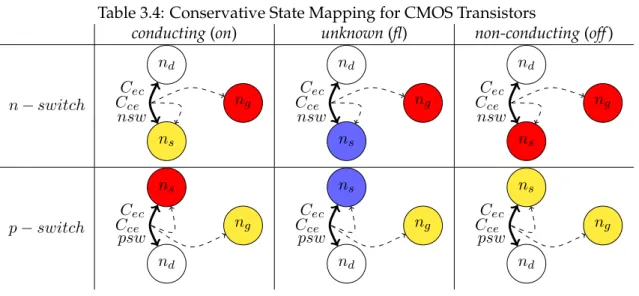
Table 3.4 shows the main differences introduced in theConservativeversion for bipolar transistors.
3. VERIFICATIONTOOL FORCIRCUITS INPOWER-DOWNMODE 3.1. Voltage Propagation Analysis
When the type of the connection isp-switch, the gate voltage level isvssand the source voltage level isvdd. This means that there is a positivesource-gatevoltage.
Forn-switchorp-switchtypes, if the source voltage level isfloatingthen the state of the connection is considered asunknown.
If the source and the gate voltage levels are equal, then the connection has a non-conductingstate.
Table 3.4: Conservative State Mapping for CMOS Transistors
conducting(on) unknown(fl) non-conducting(off)
n−switch
ns nd ng Cec Cce nsw ns nd ng Cec Cce nsw ns nd ng Cec Cce nsw
p−switch
nd ns ng Cec Cce psw nd ns ng Cec Cce psw nd ns ng Cec Cce psw
Table 3.5 shows all possible cases inConservativeversion for bipolar and MOS tran-sistors.
Table 3.5: Conservative State Mapping
source emitter voltage level vss vdd fl vss fl vdd vss fl vdd gate base voltage level vss vdd fl fl vss fl vdd vdd vss
n-switch of f of f f l f l of f f l f l on of f
p-switch of f of f f l f l f l f l of f of f on
3. VERIFICATIONTOOL FORCIRCUITS INPOWER-DOWNMODE 3.1. Voltage Propagation Analysis
3.1.3 Voltage Propagation Algorithm
After having introduced the different states, types of connections and the voltage levels for the nodes, the voltage propagation algorithm is Figure 3.4 can be formulated.
1: initialize all nodes withf loatingvoltage level.
2: initialize known nodes withvss/vddvoltage levels 3: repeat
4: for allconnections in graphdo
5: ifit is possible propagate & not propagate beforethen 6: save the connection inconnection−propagatelist
7: propagatevssvoltage level or propagatevddvoltage level
8: else
9: next connection
10: end if 11: end for
12: untilthere is no more propagation
Figure 3.4: Pseudo-Code for Voltage Propagation Algorithm
This algorithm starts with all nodes onfloatingvoltage level (line 1). Additionally, all known voltages are initialized (e.g. the supply nodes or the power-down nodes) withvss orvddrespectively (line 2).
When the voltage propagation algorithm is running, the voltage is propagated along the connections. In order to optimize the processing speed, the connections are saved in theconnections-propagatelist.
Two main rules for propagation were considered (line 7).
• Propagate vdd voltage level in direction of the connection, if the connection has
conductingstate (see Figure 3.5).
node node
on
Figure 3.5: Propagation ofvddvoltage level
• Propagatevssvoltage level in counter direction of the connection, if the connection
hasconductingstate (see Figure 3.6).
node node
on
3. VERIFICATIONTOOL FORCIRCUITS INPOWER-DOWNMODE 3.1. Voltage Propagation Analysis
In each iteration, for all connections in graphical representation (line 4), it is checked if the propagation is possible and if the connection is not inconnections-propagatelist (line 5). If condition are fulfilled, then propagation vddor vss takes place according to the previous rules and save this connection inconnections-propagatelist (line 6).
Due to the fact that connections can change their state during propagation, this cycle is repeated until there are no more connections to propagate through (line 12).
3.1.4 Working Example
The voltage propagation analysis is illustrated with the circuit represented in Figure 3.7. It has three transistors (M1,M2andM3) and four nodes(n1,n2,NvddandNvss).
circuit
graph before voltage propagation
graph after voltage propagation M1 Nvdd M2 n2 n1 M3 Nvss n1 Nvss Nvdd n2
M2−SD
psw of f
M2−DB
dio on
M1−DS
dio on M1−BD
dio on
M3−DS
nsw f l
M3−BD
dio on n1 Nvss Nvdd n2
M2−SD
psw of f
M2−DB
dio on
M1−DS
dio on M1−BD
dio on
M3−DS
nsw of f
M3−BD
dio on
(a) (b) (c)
Figure 3.7: Example of Voltage Propagation Analysis
As previously mentioned in section 3.1.1, M1 is in diode-configuration. The source
and bulk pins are connected to Nvss node and the drain pin is connected to n1. Two
diode-typeconnections are generated one from drain/gate to source and other from bulk to drain/gate. The bulk to source connection is not taken under consideration since the pins are connected to the same node.
AsM2 transistor is in a switch configuration, the source and bulk pins are connected
toNvddnode, drain pin is connected ton1 node and the gate pin is connected ton2node.
As previously stated (section 3.1.1), this transistor is a p-switchtype. Three connec-tions are considered as well as the switch relation. One connection fromNvddton1 and
one connection fromn1toNvdd, as represented in Figure 3.7(b) with a bidirectional arrow.
Onediode-typeconnection fromn1toNvddis also created. The switch relation is connected
ton2node and it was represented with a dotted arrow.
Similar connections are created forM3. In this situation the connection hasn-switch
3. VERIFICATIONTOOL FORCIRCUITS INPOWER-DOWNMODE 3.1. Voltage Propagation Analysis
also represented by a dotted arrow.
In accordance to the voltage propagation algorithm (algorithm 3.4) and after having a graph representation, it is necessary to define all the nodes withfloatingvoltage level. It was also considered thatn2 was initialized withvddvoltage level. Therefore, then2 and
Nvddare shown in red,n1in blue andNvss in yellow in Figure 3.7(b).
TheM2switch connection hasnon-conductingstate, because the gate hasvddvoltage
level and theM3 switch connection has an unknownstate, due to the fact that the gate
(switch relation) has afloatingvoltage level.
The remaining connections haveconductingstate, due to theirdiode-typenature. According to rules in voltage propagation algorithm (pseudo-code in Figure 3.4),vss
can propagate inM1diode-type connection (yellow connection in Figure 3.1.4(c)).
There-fore,n1 changed its voltage level tovss. This change in the voltage level resulted in the
M3 switch connection changing its state tonon-conducting, as is shown in figure 3.1.4(c)
3. VERIFICATIONTOOL FORCIRCUITS INPOWER-DOWNMODE 3.2. Short Circuit Analysis
3.2
Short Circuit Analysis
The short circuit analysis is responsible for finding potential short-circuit paths or short-circuit paths when the circuit is in power-down mode. The block diagram in Figure 3.8 shows the several steps compressing this analysis.
Transform Circuit to Graph
Voltage Propagation Algorithm
Depth-First Search Algorithm Fix & Reset
New Sc-path?
Valid Voltage Levels
Graph of Circuit
Graph After Voltage Propaga-tion
Yes
No Graph After
Reset & Fix
Identified Componentes
Figure 3.8: Block Diagram of Short Circuit Analysis
The dashed rectangle in the diagram represents the short circuit algorithm described in section 3.2.3, this including theV oltageP ropagationAlgorithm,Depth−F irst Search
and theF ixResetalgorithms.
TheDepth−F irstSearchalgorithm described in section 3.2.1 runs on the graph rep-resentation after the voltage propagation analysis.
3. VERIFICATIONTOOL FORCIRCUITS INPOWER-DOWNMODE 3.2. Short Circuit Analysis
If there are short circuit paths or potential short circuit paths, the result of voltage propagation analysis is not valid and in such a case an additional step is performed. The additional step is represented on Figure 3.8 with a blue box which contain theF ixReset
block described in section 3.2.2.
For this analysis short-circuit paths were considered if a path connects a positive sup-ply node (i.e., a node Nvdd) to a negative supply node (i.e., a node Nvss) and for all
connections in the path the state is conducting. Figure 3.9(a) displays an example of a short-circuit path with red connections.
There is a potential short circuit path, when there are paths that connect a positive supply node(i.e., a nodeNvdd) to a negative supply node (i.e., a nodeNvss) and the path
contains connection withconductingandunknownstate. Figure 3.9(b) shows an example of potential short circuit path with a yellow connection.
short circuit potential short circuit
n1
Nvss Nvdd n2
M2−SD psw
on
M2−DB dio on
M1−DS dio on M1−BD
dio on
M3−DS nsw of f n1 Nvss Nvdd n2
M2−SD psw
f l
M2−DB dio on
M1−DS dio on M1−BD
dio on
M3−DS nsw of f
(a) (b)
P ath: M1, M2 P ath: M1, M2
3. VERIFICATIONTOOL FORCIRCUITS INPOWER-DOWNMODE 3.2. Short Circuit Analysis
3.2.1 Depth-First Search Algorithm
In order to detect the paths in figure 3.9, a recursive depth-first search algorithm was implemented. Figure 3.10 shows how it works. The search starts from the first node and explores left half of the graph. The node is checked, if it is equal to target, then the search ends, if not the search moves to the child of the current node. If the node is a leaf, then the search tracks-back to an unexplored node.
Figure 3.10: Depth-First Search
During the search part of the analysis, it is necessary to save:
• A list containing all connections found in potential short-circuit or short-circuit.
This information is kept in thepathlist.
• A list of the paths discovered in graph representation. This information is kept in theremember-pathlist.
• A list containing all nodes visited during the path. This information is kept in the nodes-visitedlist.
The depth-first search algorithm (pseudo-code in Figure 3.11) starts by checking all nodes, that are originally defined as having a vdd voltage level (line 1). The recursive functiongo to next nodeis called (line 2) for each node.
1: for all nodes initialized withvddvoltage leveldo 2: go To Next Node (node)
3: end for
4: Check Connections(remember-path)
3. VERIFICATIONTOOL FORCIRCUITS INPOWER-DOWNMODE 3.2. Short Circuit Analysis
The pseudo-code for the function Go-To Next Node represented in Figure 3.13 and checks whether the node exists in thenodes-visited list (line 2). If the condition returns visited, then the function ends or returns to the previous node and the last connection is removed from thepathlist (line 19).
1: functionGo-To Next Node(node)
2: ifthe node not invisited−nodelistthen 3: save node invisited−nodelist
4: ifthe node not initialized withvssvoltage levelthen 5: forall out connections in nodedo
6: ifthe state of the connection isf loronthen 7: save the connection inpathlist
8: go to next node (node)
9: else
10: next connection
11: end if
12: end for
13: returnone node & remove the last node ofnode−visitedlist
14: else
15: savepathlist inremember−pathlist
16: return one node & remove last connection of pathlist & the last node of
node−visitedlist
17: end if 18: else
19: returnone node & remove last connection ofpathlist
20: end if 21: end function
Figure 3.12: Pseudo-Code forGo-T o N ext N odeFunction
If the condition returnsnot visitedthe node is saved innodes-visitedlist (line 3) and it it gets checked in order to assess if it was initially defined as having avssvoltage level (line 4). If the condition returns true then one potential short circuit or short circuit path is found. This is the reason why it is necessary to save thepathlist inremember-pathlist (line 15). If the condition returns false all connections that start on that node will be checked (line 5).
If the connection is defined with aconducting or unknown(line 6), it is saved in the
pathlist (line 7). Thego To Next Nodefunction is called and initiates a recursive cycle. If there are no more connections the function ends or returns to the previous node. Finally it is also necessary to remove the node from thenodes-visitedlist (line 13).
The recursive algorithm runs until all connections are traversed and all paths found inremember-pathare returned.
In order to identify if the paths in theremember-pathlist are potential short-circuit or short-circuit an additional function needs to be run. The corresponding pseudo-code is shown in Figure 3.13
3. VERIFICATIONTOOL FORCIRCUITS INPOWER-DOWNMODE 3.2. Short Circuit Analysis
verify if all connections haveconducting state (line 3). If the condition is fulfilled, then the path is a short-circuit (line 4), otherwise a potential short-circuit is discovered (line 6).
1: functionCheck Connections(remember−path)
2: ifall connection in path haveconductingstatethen 3: the path is a short circuit
4: else
5: the path is a potential short circuit
6: end if 7: end function
Figure 3.13: Pseudo-Code forCheck Connectionsfunction
3.2.2 Fix and Reset
According to diagram block in Figure 3.8, if no short-circuit or potential short-circuit path is discovered, the result of the voltage propagation analysis is valid and all node voltage levels have been correctly estimated.
If the depth-first search algorithm detects one or more potential short circuit or short circuit paths, then the voltage propagation analysis is not guaranteed to be valid.
The current in path will create aV dsdrop in the real circuit and all nodes lying on a potential short circuit or short circuit path won’t be able to be determined as beingvssor
vddand therefore must be reset tof loatingvoltage level.
Consider the example shown in Figure 3.14(a). Ifn2 is initialized with vss voltage
level, then the switch connection ofM2hasconductingstate (red circle in figure 3.14(b)).
Circuit First Iteration Second Iteration
M1 M2 VDD
n2
n1 M3
VSS
n1
Nvss
Nvdd
n2
M2−SD
psw on
M2−DB
dio on
M1−DS
dio on M1−BD
dio on
M3−DS
nsw of f
M3−BD
dio on n1 Nvss Nvdd n2
M2−SD
psw on
M2−DB
dio on
M1−DS
dio on M1−BD
dio on
M3−DS
nsw f l
M3−BD
dio on
(a) (b) (c)
Figure 3.14: Resetting and Fixing
After the voltage propagation algorithm runs, the internal noden1 will have a vss
3. VERIFICATIONTOOL FORCIRCUITS INPOWER-DOWNMODE 3.2. Short Circuit Analysis
Its still not clear if then1 node hasvssorvddvoltage level. According to the rules of
propagation in section 3.1.3, both switch connections (M1 orM2) can propagate because
they have aconductingstate.
In order to solve this problem, it is necessary to resetn1node tofloatingvoltage level.
The resetting can cause further potential short circuit paths. This is highlighted in yellow connection in Figure 3.14(c). To detect these new paths, it is necessary to run the voltage propagation algorithm again, but to avoid wrong paths, its necessary to fix the nodes in paths. The fixing can change some of the switch relations, as shown on Figure 3.14(c) (red circle). The switch connection ofM3 in the first iteration (Figure 3.14(b)) has
3. VERIFICATIONTOOL FORCIRCUITS INPOWER-DOWNMODE 3.2. Short Circuit Analysis
3.2.3 Short Circuit Algorithm
After the depth-first search algorithm and the additional rule have been introduced, the short circuit algorithm can be defined. Firstly, the algorithm runs the depth-first search algorithm (line 3). It is checked if new paths were found (line 4). If the condition returns true, then a reset and fix is necessary (line 5). After this step has been completed the voltage propagation algorithm runs again (line 6). If the condition doesn’t return true the algorithm ends and the result of voltage propagation analysis is valid. This cycle repeats until no new paths are found (line 8).
1: functioncheckconnections(remember−path)
2: repeat
3: Depth-First Search Algorithm
4: ifnew paths were foundthen 5: Reset and Fix the nodes in path
6: Voltage Propagation Algorithm
7: end if
8: untilno new paths were found
9: end function
3. VERIFICATIONTOOL FORCIRCUITS INPOWER-DOWNMODE 3.3. Stress Analysis
3.3
Stress Analysis
The stress analysis is responsible for finding asymmetrical stress conditions in struc-tures. The diagram block shown in Figure 3.16 describes the tasks executed by this anal-ysis.
Structure Recognizer
Stress Algorithm Power-Down Processor
Identified Structures
Structures Detected Stress Graph
Representation after
Voltage Analysis Rules File
Net-List File without Power-Down Transistors
Net-List File
Figure 3.16: Block Diagram of Stress Analysis
The analysis starts by removing the power-down switches in the netlist file. To do this a Power-Down Processor is needed. Figure 3.17 shows an example illustrating the need for removing the power-down switches so that the structure recognizer block can identify matched structures correctly.
M2 M1
M3 npwd+
power-on
M2 M1
Figure 3.17: Remove Power-down Switches
The algorithm inside of thestructure recognizerblock identifies structures such as cur-rent mirrors and diffecur-rential pars.
In order to detected the problems in these structures a file containing rules will be necessary.
3. VERIFICATIONTOOL FORCIRCUITS INPOWER-DOWNMODE 3.3. Stress Analysis
Table 3.6: Structure Rules File
Structure Rules
M2 M1
• drain ofM1must equal the drain ofM2
• gate ofM1must equal the gate ofM2
• source ofM1must equal the source ofM2
M3 M4
• drain ofM3must equal the drain ofM4
• gate ofM3must equal the gateM4
• source ofM3must equal the source ofM4
The Stress Algorithm block contains the stress algorithm described in section 3.3.1. This stress algorithm compares the voltage levels in each node of graph representation with the rules of structures, thus allowing to detect asymmetrical stress conditions. The analysis returns structures where asymmetrical stress exists.
In Figure 3.18(a) it can be seen that the simple current mirror with red and differential par with blue colors were successfully identified.
Figure 3.18(b) shows the graph representation after voltage propagation analysis. In this simple current mirror, asymmetrical stress conditions were detected because there is a mismatch at the drains ofM1andM2with different voltage levels in the graph
representation.
3. VERIFICATIONTOOL FORCIRCUITS INPOWER-DOWNMODE 3.3. Stress Analysis
M3 M4
n1 VDD M1 M2 M6 n3 M5 n2 VSS npwd nbias
nin+ nin−
(a) Schematic
nv dd
nv ss npwd
n1
n3 n2
nin− nin+
nbias
CM6 nsw of f CM5
dioon CM3
psw f l
CM4 psw
f l CM2
psw of f CM1
psw on
(b) Transient Simulation
Figure 3.18: Example of Stress Analysis
3.3.1 Stress Algorithm
The stress algorithm starts by reading the rule file for the structures (line 1). For each structure, a search is performed for each corresponding nodes (line 3).
A comparison between the defined rules and the estimated voltage levels is made. If the comparison returns as all the rules being fulfilled (line 4), then the structure does not have asymmetrical stress conditions (line 5). If one or more rules are not violated, then asymmetrical stress conditions can occur in the structure (line 7).
1: Read Rules File
2: for allidentified structuresdo
3: find the nodes of structure in graph representation 4: ifthe rules defined for this structure are fulfilledthen 5: No asymmetrical stress conditions are found
6: else
7: Asymmetrical stress condition are found
8: end if 9: end for
3. VERIFICATIONTOOL FORCIRCUITS INPOWER-DOWNMODE 3.4. All Program
3.4
All Program
The program was designed to ensure that each analysis can be called separately. The implementation was made in C++.
The block diagram shown in Figure 3.20 represents the implementation of the verifi-cation tool with all relevant data exchange between analysis.
NetList File
Structure Recognizer
Transform Circuit to Graph
Voltage Propagation Stress
Short Circuit Results
Cadence Virtuoso Design Framework Previously
Implemented
Newly Implemented
Structure Recognizer Power-Down Processor
Detected simple devices
Graph of Circuit
Graph after Voltage Propagation
Voltage Levels and States
Detected Structures with
Stress Net-List File
without Power-Down Transistors
Detected Structures
List of Paths Graph after
Reset and Fix
Figure 3.20: Bock Diagram of Verification of Power-Down Mode Program
3. VERIFICATIONTOOL FORCIRCUITS INPOWER-DOWNMODE 3.5. Summary
runs the voltage propagation algorithm described in section 3.1.3. As result, a graph rep-resentation after voltage propagation is obtained. This is used by theShort-Circuitblock. As previously mentioned in section 3.2.2, if no paths are found then the voltage propa-gation results are valid. If there are paths, then theShort-Circuitblock returns the graph representation after resetting and fixing of nodes (see section 3.2.2). The voltage propa-gation block receives this graph and runs the voltage propapropa-gation algorithm (Algorithm 3.4) again.
In the right part of the diagram block, power-down transistors are removed by the Power-Down Processor block (see section 3.3) from the net-list file. Thus, structures cor-rectly identified by theStructure Recognizerblock can be used inStressblock. It receives the returned voltage levels from theVoltage Propagation block and return the structures where stress conditions can occur.
The Results block contains all possible results. It includes the expected node volt-age levels, the expected transistor state, paths returned by short-circuit analysis and the structures with stress conditions. TheResults block was prepared to be integrated into CADENCE enviroment.
3.5
Summary
In this chapter the constituent analysis modules for the verification tool were pre-sented.
These analysis includes the voltage propagation, the short-circuit and the stress anal-ysis. For each of them a block diagrams containing the operation method and examples with graph representation were shown.
In the voltage propagation analysis, the corresponding graph representation as well the algorithm needed to identify the voltage along the connections were described.
After this analysis, it is possible guarantee the estimate node voltage levels with the short-circuit analysis.
4
Results
The results obtained with the verification tool in three circuits equipped with power-down mode are presented and in this chapter.
In section 4.1, the circuit is a two-stage amplifier in buffer configuration. For this circuit all results of the analysis are shown with graphical representations.
To ensure that the program works in MOS and bipolar technologies, section 4.2 presents the results for a BiCMOS circuit.
The verification tool was tested on a few industrial circuits. Section 4.3 shows the results of one of these tests.
Sections 4.1-4.3 demonstrate the results obtained from the comparison between the voltage propagation analysis and DC analysis obtained from simulation.
4. RESULTS 4.1. Two-stage Amplifier
4.1
Two-stage Amplifier
The first working example is shown in Figure 4.1, where the circuit is equipped with three power-down switchesM1,M2,M3and has 10 components and 9 nodes.
The backgate connections are not drawn in the circuit, but for NMOS devices they are connected tonvssand for PMOS devices they are connected tonvdd.
M10
M5 M6
n1
M8 M7
n2
nout
nvss nvdd
M9 n3
M1 M2 M3
M4 npwd
nbias
nin
power-down switches
differential pair
Figure 4.1: Two-Stage Amplifier Schematic
The graph representation of the circuit before voltage propagation analysis is shown in Figure 4.2. Since the corresponding bulk to source and bulk to drain connections never propagate they can be left out of the graph representations.
In order to put the circuit in power-down mode, thenpwd node needs to be defined
with vss voltage level. Thus, the nvdd hasvdd voltage level are represented in red on
Figure 4.2. The nodesnvssandnpwdhavevssvoltage level and are represented in yellow.
The other nodes havef loatingvoltage level and are represented in blue.
M8 is in diode configuration, which means its in aconductingstate. SwitchesM1,M2
andM3connections have aconductingstate because their gates have avssvoltage level.
These are represented in Figure 4.2 with red circles. The remaining connections have
4. RESULTS 4.1. Two-stage Amplifier
nv dd
nv ss npwd n1 n2 n3 nout nin nbias
CM3 psw
on CM10
psw f l
CM9 nsw
f l CM8
dio on CM7
nsw f l CM5
psw f l
CM6 psw
f l CM4
psw f l CM1
psw on
CM2 psw on
Figure 4.2: Graph Representation of Two-Stage Amplifier before Voltage Propagation Analysis
Figure 4.3 shows the results after the voltage propagation has run. As a result a few voltage levels have to propagate and according to state mapping in section 3.1.2 some connections change their state. This is shown in Figure 4.3 with red circles.
Noden2hasvssvoltage level, whilenout,ninandnbiashavevddvoltage level.
The switchesM4,M5,M6,M7 andM10connections have non-conductingstate, while
M9switch connection has anunknownstate.
In order to validate the voltage propagation results, a short-circuit analysis needs to be run in order to detect potential short-circuit and/or short-circuit paths.
In power-down mode a potential short circuit may occur with pathM3 andM9.
Yel-low connections in Figure 4.3 show the path in graph representation. TheM3connection
has aconductingstate because its gate has avssvoltage level and the state ofM9
4. RESULTS 4.1. Two-stage Amplifier
nv dd
nv ss npwd n1 n2 n3 nout nin nbias
CM3 psw
on CM10
psw of f
CM9 nsw
f l CM8
dio on CM7
nsw of f CM5
psw of f
CM6 psw
of f CM4
psw of f CM1
psw on
CM2 psw on
Figure 4.3: Graph Representation of Two-Stage Amplifier after Voltage Propagation Anal-ysis
Then the node voltage are reevaluated according to the procedure described in section 3.2.2. Because of this, nout node was fixed with a floatingvoltage level and the voltage
propagation is run again in order return a new graph representation.
The figure 4.4 shows the results after the second run of voltage propagation algorithm. Thenoutnode changes its voltage level tofloating, the state ofM6 connection changed to
4. RESULTS 4.1. Two-stage Amplifier
nv dd
nv ss npwd n1 n2 n3 nout nin nbias
CM3 psw
on CM10
psw of f
CM9 nsw
f l CM8
dio on CM7
nsw of f CM5
psw of f
CM6 psw
f l CM4
psw of f CM1
psw on
CM2 psw on
Figure 4.4: Graph Representation of Two-Stage Amplifier after Short Circuit Analysis
The stress analysis identified two structures and they are represented in figure 4.4 with dashed rectangles.
According to the rules of these two structures, in the simple current mirror asymmet-rical stress conditions were detected, since there is a mismatch at the drains ofM7 and M8with different voltage levels. Similarly, in the differential pair the drains and gates of M5andM6have different voltage levels and asymmetrical stress conditions can occur.
4. RESULTS 4.1. Two-stage Amplifier n1 n2 nout nvss nvdd n3 M1 on M2 on M3 on M4 of f M5 of f M6 f l M7 of f M8 on M9 f l M10 of f npwd nbias nin power-down switches differential pair current mirror
Figure 4.5: Two-Stage Amplifier with Verification Tool
In order to check if the node estimated values are valid, a comparison with the DC analysis of the circuit in power-down was made.LiberalandConservativeversions of state mapping were used (see section 3.1.2) and both produced the same results. The circuit was implemented in .32µmtechnology and using a 3.3 volt supply. Table 4.1 shows the expectedvssandvddnodes. The DC analysis shows a maximum relative error is 0.2%.
Error(%) =
(
100∗(Vdc/Vdd) if voltage level isvss
100∗(Vdd−Vdc)/Vdd if voltage level isvdd
Table 4.1: Nodes expected withvssandvddVoltage Level of Two-Stage Amplifier
Node Name nvdd nbias nin nvss n2 npwd
Voltage Propagation vdd vdd vdd vss vss vss
DC Analysis [V] 3.3 3.3 3.3 0 0.006 0
Error [%] 0 0 0 0 0.2 0
The table 4.2 shows the expected states of transistors and the relevant comparison with the DC analysis. For the purpose of this comparison it was assumed that if theVgs
4. RESULTS 4.1. Two-stage Amplifier
than 1, then the state of transistor innon-conducting.
State=
(
Vgs/Vth >1 conducting Vgs/Vth <1 non−conducting
As result M1, M2 and M3 transistors after the voltage propagation algorithm were
expected to beconducting. This is verified by the DC analysis because theirVgs voltage
drop is 8 times higher than theVthvoltage. Thenon-conductingtransistors are also correct
becauseVgsoverVthis zero.
Table 4.2: Expected State of Transistors of Two Stage Amplifier
State conducting non-conducting
4. RESULTS 4.2. BiCMOS
4.2
BiCMOS
Figure 4.6 represents a BiCMOS circuit combining CMOS and bipolar technology on the same circuit. It contains 7 bipolar, 5 MOS transistors and 9 nodes. In the source 2.1 volt in supply was used. Table 4.3 shows the current consumed of this circuit in normal operation (power on).
In order to prove that the verification tool works with bipolar transistors one power-down switch was added (M5 in Figure 4.6). This turns off the current throughM3 and M4, but the current can flow in the red paths in Figure 4.6.
n6 n5
n2
nout nvdd
nvss
M5
on
n4 n3
ninn ninp nbias npwd−
n1
power-down switch
Figure 4.6: BiCMOS Circuit With One Power-Down Switch
Table 4.3: Current Consumption (DC) Figure 4.6 Figure 4.8
power-on 61,5µA 61,5µA
4. RESULTS 4.2. BiCMOS
The graph representation in Figure 4.7 shows that all these paths were successfully identified by the verification tool. As a result all currents are not reliably turned off and the estimated node voltages have errors. The DC analysis shows that the current values changed with theM5 power-down switch (table 4.3 power-off).
Most of these potential short circuit occurs because thenbiasnode hasf loatingvoltage
level. This controls the state ofM6switch connection which isunknown.
nv dd
nv ss npwd−
n2
n4
n5 n6
nout n3 n1 nbias ninp ninm CM4−sd
psw of f
CQ5−ec psw
f l
CQ4−ce nsw f l CQ4−bc
dio on CM2−sd
psw f l CM2−db
dio on
CQ4−be dio on CQ2−ce
dio on CM1−sd
psw f l
CM1−db psw
on
CQ3−be dio
on
CQ1−ce dio on CQ3−ce
nsw f l
CQ3−bc dio
on
CQ7−ec psw
f l CR1 dio on
CQ7−cb dio
on CQ6−cb
dio on CQ7−eb
dio on CQ6−ec psw f l
CQ5−eb dio
on CdioQ6−eb on
CM3−sd psw
on
CM3−sd dio on
CM6−ds nsw
f l
CM5−DS psw
on
4. RESULTS 4.2. BiCMOS
To overcome this situation one more power-down switch was added onto the BiC-MOS circuit (M7in Figure 4.8). The circuit now contains two power-down switches
indi-cated by dotted black rectangles. For the new transistor two connections fromnbiastonvss
are created (yellow bidirectional arrow in Figure 4.9), these connections are controlled by thenpwd+node which should be assignedvddvoltage level for power-down.
For this circuit, no potential short-circuit or short-circuit path is found by the verifi-cation tool and the DC analysis shows that the current changed approximately to zero (power-off table 4.3). This can be seen in the graph representation in Figure 4.9. It is pos-sible conclude that all currents are safely turned off and the calculated node voltages are accurate.
The transistors state as well as the detected floating nodes (blue line) returned by the verification tool are shown in Figure 4.8.
n6 n5 n2 nout nvdd nvss n4 n3 ninn ninp nbias npwd−
npwd+
n1 M3 of f M4 of f M1 f l M2 f l M6 of f M7 on Q5 of f Q1 on Q2 on Q3 of f Q4 of f Q7 of f Q6 of f power-down switch
4. RESULTS 4.2. BiCMOS
nv dd
nv ss npwd−
npwd+ n2
n4
n5 n6
nout n3 n1 nbias ninp ninm CM4−sd
psw of f
CQ5−ec psw
of f
CQ4−ce nsw of f CQ4−bc
dio on CM2−sd
psw f l CM2−db
dio on
CQ4−be dio on CQ2−ce
dio on CM1−sd
psw f l
CM1−db psw
on
CQ3−be dio
on
CQ1−ce dio on CQ3−ce
nsw of f
CQ3−bc dio
on
CQ7−ec psw
of f CR1 dio on
CQ7−cb dio
on CQ6−cb
dio on CQ7−eb
dio on CQ6−ec psw of f
CQ5−eb dio
on CdioQ6−eb on
CM3−sd dio
on
CM3−sd dio on
CM6−ds nsw
of f
CM5−DS psw
on
CM7−ds nsw
on
Figure 4.9: Graph Representation of BiCMOS Circuit with Two Power-Down Switches After Verification Tool
Table 4.4 shows the comparison of the node voltages generated by the verification tool and the DC analysis. For BiCMOS circuit it is possible conclude that the maximum relative error is 15,7%.
These results happen since the sizing of the transistors are not considered for the verification tool.
Table 4.4: Expected Voltage Levels in BiCMOS Circuit
Node nvdd n1 n2 n3 nbias nvss n5 n6 Verification Tool vdd vdd vdd vdd vdd vss vss vss
DC Analysis [V] 2.1 1.766 2.1 2.1 2.1 0 0.231 0.231
![Figure 2.1: Differential Stage With Power-Down Switch [ZG12]](https://thumb-eu.123doks.com/thumbv2/123dok_br/16580461.738526/24.892.257.590.135.516/figure-differential-stage-with-power-down-switch-zg.webp)