Design and Analysis of New Modified Feedthrough Logic (MFTL)
Circuits Using Carbon Nanotube Field Effect Transistor
(CNTFET)
Sneha Meryn Thomas
1, Rakesh S
21
(Department of Electronics and Communication Engineering, Mangalam College of Engineering, MG University, Ettumanoor, Kerala-686631)
2
(Asst. Prof, Department of Electronics and Communication Engineering, Mangalam College of Engineering, MG University, Ettumanoor, Kerala-686631)
ABSTRACT
It is a challenging task for a VLSI design engineer to develop low power VLSI circuits, without sacrificing its performance. Feedthrough Logic (FTL) is a new technology which could be considered better than the existing technologies for improving circuit efficiency. Modified Feedthrough Logic (MFTL), offers a better power factor than the FTL logic structures, and also shows an improvement in the speed factor. But the scenario again changes when the design extends to nano scales of device dimension, where many factors which were neglected otherwise need to be given more importance. To avoid or minimize problems like hot carrier effects, electro migration, drain induced barrier lowering and other issues that becomes prominent in nano scale MOSFET‟s, Carbon Nanotube Field Effect Transistor (CNTFET) is considered to be a promising candidate in future integrated circuits. Hence this work extends the advantages of MFTL logic into nano level by incorporating CNTFETs in place of MOSFETs. The modifications have been implemented using CNTFETs of 16nm technology from HSPICE library on a 10 chain inverter stage, an 8 bit RCA and a Vedic multiplier and performance factors like PDP and ADP are compared to that of the conventional MOSFET circuits.
Keywords
– CNT, Domino logic, FTL, MFTLI.
Introduction
When considering the circuit design styles put forward in the last couple of decades, it can be seen that power is the factor that gets compromised for attaining the overall circuit efficiency. Some of the different common methods employed include the use of multi threshold voltages for different circuit portions, using dual supply voltages as needed [8,9,10,11] etc. But in all such cases, it is seen that power factor gets traded for attaining efficiency.
However the development of FTL proved to bring a better change, as it provides improved power and speed factors compared to the existing circuit styles. It provides high performance operation for delay critical circuit like arithmetic or pipelining circuit [2,3]. Domino logic that is employed primarily to overcome the cascading issues of dynamic logic blocks, hold to be the basic principle of FTL logic. In addition, the main feature of FTL is its ability to evaluate the final output before all the inputs have a valid value or voltage level. This can be considered as the factor that improves the speed of the circuit. This pre-evaluation is possible because of the presence of the clock, which acts as the control signal. Also, with respect to the short comings of domino logic like inability to provide non inverting logic, problem of charge sharing, monotonic nature
of output and requirement of additional inverter at output [2, 3,12,13], FTL can be used to overcome them gracefully.
Again, from the previous works carried out [1]., Modified FTL (MFTL) circuit families provide better PDP as compared to the existing FTL. For MFTL, the working principle is the same as for existing FTL and the difference comes structurally as explained in Section II. Hence MFTL also has the advantages of FTL style.
As scaling down of dimensions have become a necessity and reality in the modern scenario of circuit designs, new challenges are put forward to the designer including dealing with issues like electro migration as in the case of interconnects and hot carrier effects, drain induced barrier lowering and so on in case of MOSFET‟s. Hence better options and architecture for new interconnects and alternative for MOSFETs must be generated. Carbon Nanotube Field Effect Transistor (CNTFET) is a promising candidate for future integrated circuits because of its excellent properties like near ballistic transport [4], high carrier mobility and easy integration of high-k dielectric material [4, 5, 6, 7], Hence this work extends the advantages of MFTL logic into nano level by incorporating CNTFETs in place of
MOSFETs. The modifications have been
from HSPICE library on a 10 chain inverter stage, an 8 bit RCA and a Vedic multiplier and performance factors like PDP and ADP are compared to that of the conventional MOSFET circuits [14].
Section 2 explains the working principle of the MFTL circuits. Section 3 describes the principle of operation of LP-MFTL circuits. Section 4 gives a detailed analysis explanation of the MFTL and LP-MFTL logic styles when implemented using CNTFETs, through extensive simulation on HSPICE platform. Section 5 gives a glossary of the advantages, disadvantages and applications of MFTL logic.
II.
PRINCIPLE OF MFTL OPERATION
Consider the block diagram of MFTL structure, as extended from existing FTL structure [Fig 1].Fig 1 MFTL structure
For FTL, the pull down network is connected directly to ground, whereas in MFTL the pull down network is connected to ground through additional NMOS transistor Ta. The gate of NMOS is driven by VDD as gate source voltage. Similar to FTL, following the domino logic, MFTL also uses a clock as the control signal.
The principle of operation of MFTL is as follows: There are two phases of operation depending upon the value of the clock namely. Precharge phase (CLK=0) and Evaluation phase (CLK=1). During Evaluation phase (clock goes „HIGH‟), output is pulled to „LOW‟ through reset transistor Tr and during Precharge phase (clock goes „LOW‟), the output is generated conditionally according to the given set of inputs with additional transistor Ta which is always „ON‟. The purpose of the additional transistor Ta is to increase the dynamic resistance of the pull down network, which in turn causes the output node to discharge to a VOL value that is greater than that of the existing FTL. This trade-off in VOL results for less high-to-low propagation delay from VTH to VOL, thus reducing the overall delay. Also, increased value of VOL reduces power consumption,
as the dynamic power dissipation of a digital circuit is given by
P dynamic = α.CL.VDD .V(x).Fclk (1)
Here, α is the switching factor, CL is the load capacitance, VDD is supply voltage, Fclk is the maximum operating frequency and V(x) is the power delivered by the source during low to high transition. Increased value of VOL reduces V(x) in MFTL. Therefore, modified FTL has lower dynamic power consumption than in existing FTL
III.
PRINCIPLE OF LP-MFTL OPERATION
For LP-MFTL structure also, the connection to the ground from the NMOS block (pull down network) in existing LP-FTL structure is replaced with additional NMOS transistor Ta which is then connected to ground.Consider the block diagram of LP-MFTL structure [Fig 2], as extended from existing LP-FTL structure.
Fig 2 LP-MFTL structure
Power reduction in LP-FTL logic is obtained with the additional PMOS transistor TP2 that comes in series with TP1 that actually reduces VOL. The operation of this circuit is also controlled by the clock signal. When the clock signal, „CLK‟ is HIGH (evaluation phase) output node is pulled to ground (LOW) through Tr and when CLK goes LOW (precharge phase) output node charges (HIGH) through TP1 and TP2. During this phase, the reset transistor, Tr is turned off and the output node conditionally evaluates to logic high (VOH) or low (VOL) depending upon input to NMOS block. If the NMOS block is turned off, then there exists a high resistance path from the output node to ground and hence, output node gets pulled toward VDD i.e. VOH =VDD, otherwise it remain at logic low i.e. VOL. However for the output to discharge to a complete LOW value, it requires the occurrence of a subsequent evaluation phase. As the two PMOS
Existing LP-FTL grounded by Ta
transistors, TP1 and TP2 are in series the voltage at drain of TP1 is lower than VDD causing a significant reduction in dynamic power consumption compared to existing FTL but due to the insertion of PMOS transistor TP2 propagation delay of the existing LP-FTL in Fig. 2, increases. Despite the above sited advantages of FTL and MFTL logic, it suffers from a non-zero logic low condition.
Low power proposed modified FTL (LP-MFTL), has an NMOS transistor Ta connected as shown in Fig. 2. When clock goes „HIGH‟, output is pulled to „LOW‟ through reset transistor Tr. When clock goes „LOW‟; the output is generated according to the given set of inputs with additional transistor Ta always „ON‟. For LP-MFTL, due to the insertion of PMOS transistor TP2 propagation delay increases.
IV.
PERFORMANCE ANALYSIS OF
NEW LOWER POWER MFTL
STRUCTURE USING CNTFET
4.1 Results for Inverter
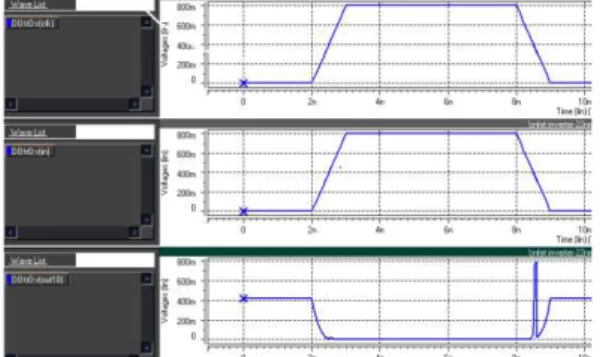
Fig 3 shows the timing diagram for a 10 chain MFTL inverter using CNTFETs, where the first slot represents the clock signal „clk‟, the second slot represents the input „in‟ and the third slot the output „out10‟. When „clk‟ = 0 and „in‟ =0, the output „out10‟ represents LOW (approximately = 700mV, showing a greater VOL value).
Fig.3 Timing diagram for 10 chain MFTL inverter.
TABLE I PDP comparison for FTL, MFTL in CNTFET (10 Chain Inverter)
Type Power (uW)
Delay (ps)
PDP(uW x ps) x 10^- 14
FTL 32.3 486.7 1.57
MFTL 19.06 271.8 0.518
From Table I for 10 inverter chain using FTL and MFTL logic using CNTFETs, it can be viewed that for the proposed modified MFTL structure, there is a significant reduction in power consumption, as well as a noticeable increase in the speedup factor. In
other words, from the analysis, a 39% decrease in power and an improvement by 42% for speed factor could be observed. As a result MFTL circuit using CNTFETs in nano scale of dimension holds a better PDP compared to the existing FTL structure.
TABLE II. ADP comparison for FTL, MFTL (10 chain inverter)
Type No; of transistors
Delay (ps)
ADP(nm2 x ps) x 10^- 25
FTL 30 486.7 9.3
MFTL 40 271.8 6.9
In contrary to the ADP comparison for inverter chain using MOSFETs [1], while comparing the ADP of FTL and MFTL circuits using CNTFETs in nano scale, one can notice that the requirement of additional number of transistors gets compensated by the improved speedup factor in the nano regime, thus MFTL 10 chain inverter circuit showing a better ADP.
4.2 Results for 8 bit RCA
For obtaining a justifiable output, for all the circuit structures, same set of input is used which goes like Ai =0.8 V for 5 ns, Bi =0.8V for 5ns (where I = 1 to 8) and C1 =0. Then the output file obtained for different FTL RCA structures using CNTFETs are shown below.
Fig.4 Output file for 8 bit FTL RCA
Fig.6 Output file for 8 bit LP- MFTL RCA
TABLE III. PDP comparison for 8 bit RCA using CNTFET
Type Power (uW)
Delay (ps)
PDP(uW x ps) x 10^- 15
FTL 24 91.88 2.2
MFTL 15.03 52.18 0.784
LP -MFTL
7.87 87.00 0.68
From Table III for 8 bit RCA using FTL, MFTL logic and LP-MFTL logic using CNTFETs, it can be viewed that for the proposed modified MFTL structure, there is a significant reduction in power consumption, as well as a noticeable increase in the speedup factor. As a result MFTL circuit using CNTFETs in nano scale of dimension holds a better PDP compared to the existing FTL structure. At the same time the modification when applied to the existing LP-FTL structure, yields a further reduction in power, hence a better PDP than the FTL and MFTL structures is obtained.
4.3 Results for Vedic Multiplier
“Urdhva iryagbhyam” sutra is the algorithm on which the Vedic Multiplier works. From earlier times onwards, these algorithms are being used, mainly for the multiplication of two numbers in the decimal number system. However, this sutra may be applied to all cases of multiplication. The literal meaning of this algorithm is “Vertically” and “Crosswise”. It is based on a new concept in which the concurrent addition of the partial products. generates all partial products.
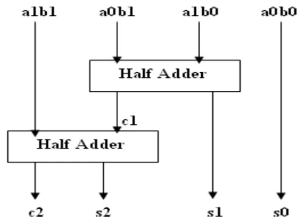
The 2X2 Vedic multiplier module is
implemented using four input AND gates & two half-adders which is displayed in its block diagram in Fig 7
Fig 7 Block diagram of 2 x 2 bit Vedic Multiplier
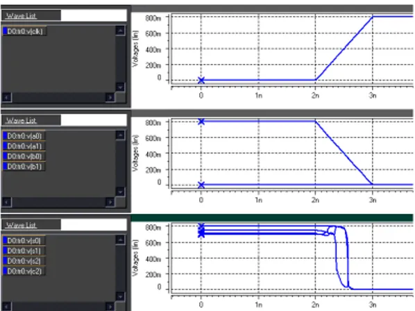
Fig 8 shows the timing diagram for a 2 x 2 MFTL Vedic Multiplier, obtained from DSCH which is a Schematic tool, where the result can be obtained directly by drawing the required circuit diagram. This tool helps to verify the correctness of the design as the circuit can be directly simulated and the working can be viewed through checking output LEDs turning ON and OFF according to inputs, whereas in HSPICE where the designer can depend only on the output graphs and output files obtained.
Fig 8 Timing diagram of 2 bit Vedic Multiplier in MFTL (DSCH).
Fig 9 Timing diagram of 2 bit Vedic Multiplier in FTL
Fig 10 shows the output file obtained from HSPICE for Vedic multiplier in FTL for the inputs as (a0 ,a1, b0, b1) HIGH for a period of 2ns. Similarly Fig 11 and Fig 12 show the output files for 2 bit Vedic Multiplier using MFTL and LP-MFTL structures.
Fig.10 Output file for 2 bit FTL Vedic Multiplier using CNTFET
Fig.11 Output file for 2 bit MFTL Vedic Multiplier using CNTFET
Fig.12 Output file for 2 bit LP-MFTL Vedic Multiplier using CNTFET
Table IV shows the PDP comparison for Vedic multiplier using CNTFET in FTL, MFTL and LP-MFTL structures.
TABLE IV PDP comparison for Vedic Multiplier using CNTFET
Type Power (uW)
Delay (ps)
PDP(uW x ps) x 10^- 15
FTL 23.37 68.78 1.6
MFTL 21.62 66.76 1.45
LP MFTL
20.71 68.75 1.4
From Table IV, PDP comparison for the three structures namely FTL, the proposed MFTL and the proposed LP MFTL is obtained. Here also better PDP values are obtained for the proposed structures.
V.
CONCLUSION
The advantages of MFTL logic includes those as for FTL as already cited in Section 1. In addition, MFTL provides faster circuits with lower power dissipation. Also, the circuit for low power improves dynamic power consumption as compared to the existing Feedthrough Logic circuits .The result comparison of Table III points to the advantage obtained in power and delay when the FTL, MFTL and LP-MFTL 8 bit RCA structures are extended to the nano regime. A clear difference in performance can be obtained by analyzing the Power Delay Product of each structure. For both cases as from Table III and Table IV, better PDP is obtained for the LP-FTL structure. From this analysis we can conclude that the advantages of using the proposed MFTL logic could be effectively extended to nano scale of dimensions employing CNTFETs.
Despite these performance advantages, MFTL circuit suffers from certain disadvantages like reduction in noise margin, direct path current and a non-zero low output voltage which occurs due to contention between PMOS and NMOS in the evaluation block. And the inclusion of additional NMOS transistor is needed making the circuits more area greedy while using MOSFETs.
However, due to better power and delay factors, MFTL based circuits can be employed in high fanout and high switching frequency circuits. Also, MFTL logic can be used in cascaded stages, differential style, as well as multiple output logic with iterative networks. MFTL logic can also be used effectively in nano scale dimensions using CNTFETs.
REFERENCES
[1] Sneha Meryn Thomas, Rakesh S
[2] Sauvagya Ranjan Sahoo1, Kamala Kanta Mahapatra,”Performance Analysis of modified Feedthrough Logic for Low Power and High Speed” in IEEE – ICAESM2012. [3] V. Navarro-Botello, J. A. Montiel-Nelson,
and S. Nooshabadi, “ Analysis of high performance fast feedthrough logic families in CMOS,” IEEE Trans. Cir. & syst. II, vol. 54, no. 6, Jun. 2007, pp. 489-493.
[4] Ginto Johnson and Vinod Pangracious “CNT
Based Channel Interconnect for CMOS Devices” CCSIT 2012, Part II, LNICST 85, pp. 585–595, 2012
[5] Subhajit Das, Sandip Bhattacharya,
Debaprasad Das “Design of Digital Logic Circuits using Carbon Nanotube Field Effect Transistors” International Journal of Soft Computing and Engineering (IJSCE) ISSN: 2231-2307, Volume-1, Issue-6, December 2011
[6] Roberto Marani & Anna Gina Perri
“Simulation of CNTFET digital circuits: a Verilog-A implementation” IJRRAS 11 (1) April 2012 Volumes/Vol11Issue1
[7] Ali Ghorbani and Mehdi Sarkhosh and
Elnaz Fayyazi and Neda Mahmoudi and Peiman Keshavarzian “A novel full adder cell based on Carbon Nanotube Field Effect Transistors” International Journal of VLSI design & Communication Systems (VLSICS) Vol.3, No.3, June 2012.
[8] Subodh Wairya, Rajendra Kumar Nagaria, Sudarshan Tiwari “New Design Methodologies for High-Speed Mixed-Mode
CMOS Full Adder Circuits”, International
Journal of VLSI design & Communication Systems (VLSICS) Vol.2, No.2, June 2011. [9] QiWang and Sarma and B.K. Vrudhula ,
“Efficient Procedures for Minimizing the Standby Power in Dual VTCMOS Circuits”. [10] S.Vangal, Y. Hoskote, D. Somasekhar, V.
Erraguntla, J. Howard,
Ruhl,V.Veeramachaneni, D. Finan, S.
Mathew, and N. Borkar, “A 5-GHz floating point multiply-accumulator in 90-nm dual
VT CMOS,” in Proc. IEEE Int. Solid-State Circuits Conf., San Francisco, CA, Feb.2003, pp. 334–335
[11] R. K. Krishnamurthy, S. Hsu, M. Anders, B. Bloechel, B. Chatterjee,M. Sachdev, and S. Borkar, “Dual supply voltage clocking for 5-GHz 130-nm integer execution core,” in Proc. IEEE VLSI Circuits Symp., Honolulu, HI, Jun. 2002, pp. 128–129
[12] J. M. Rabaey, A. Chandrakasan, and B. Nikoli‟c, Digital Integrated Circuits: A Design Perspective 2 edition
[13] Sung-Mo Kang, Yusuf Leblebici, CMOS
digital Integrated Circuits analysis and design
[14] HSPICE® Simulation and Analysis User


