978-1-4799-5743-9/14/$31.00 ©2014 IEEE
A Microprogrammed Control Path Architecture
for an Embedded IEEE 1149.1 Test Coprocessor
Ukbagiorgis I. Gebremeskel, José M. M. Ferreira ([email protected], [email protected])
Buskerud and Vestfold University College, Kongsberg, Norway
Abstract—This paper proposes a test coprocessor for a 32-bit MicroBlaze CPU core. A microprogrammed architecture is used to implement the coprocessor control path, offering a flexible solution that ensures a straightforward expansion of the test command set. The current version supports a set of SVF-like commands that is able to control one built-in IEEE 1149.1 boundary-scan infrastructure. The proposed test coprocessor is useful in a wide range of online test applications, and namely in the case of mission-critical embedded systems, where online fault detection and diagnosis become particularly important.
Keywords -Boundary-scan, embedded systems, test coprocessor, micro-programmed architectures, FPGA, MicroBlaze
I. INTRODUCTION
Over 20 years of wide industry acceptance enabled the development of many test controllers for the IEEE 1149.1 Standard Test Access Port and Boundary-Scan Architecture [1]. These test controllers range from high-end automated test systems to dedicated chips that are embedded into custom solutions, and support a variety of test specification formats, from SVF (Serial Vector Format [2]) to dedicated command sets. The later approval of IEEE 1149.6 [3], and more recently the approval of IEEE 1149.7 [4:7], reinforced the importance of looking into the expansion of the test commands commonly supported in the IEEE 1149.1 world, so as to fully exploit the potential offered by a much broader application domain that includes debugging and embedded instruments [5:8].
The range of tools available to implement 1149.7 is yet very limited, which delays the identification of additional features needed by enhanced test controllers capable of handling 1149.1 / 1149.6 / 1149.7 / P1687 test programs. On the other hand, the ever increasing integration density that enables SoC / SiP / PiP, brings additional interest to the development of embedded test coprocessors [6], tailored to the specific requirements of each system or application domain. A standard Fast Simplex Link (FSL [9]) was used to interface the proposed coprocessor to a 32-bit MicroBlaze CPU, and the experimental prototype was implemented in a Spartan 6 Xilinx FPGA. The following section introduces the subject of 1149.x test controllers and summarises their functional requirements. The control path and the complete test coprocessor architecture are presented in section III. Section IV addresses the test command design process, from ASMD chart specification to microprogram memory content. Section V presents experimental data and provides information on performance and logic resource usage. A final section informs about future research plans, and is followed by a list of references.
II. CONTROL OF 1149.X TEST INFRASTRUCTURES
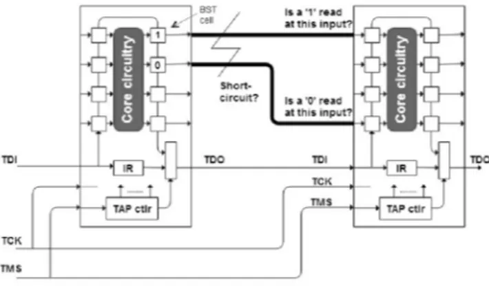
The set of boundary-scan (BS) test cells is at the core of the IEEE 1149.x standards. By controlling the operating mode of these cells, and scanning in an appropriate test pattern, it is possible to set up the logic conditions necessary to activate and detect any structural fault.
Fig. 1. Using the boundary-scan cells to check for a short-circuit fault.
The short circuit shown in figure 1 may be detected by carrying out a sequence of elementary test operations comprising the following steps (assuming that all BS cells are initially in transparent mode):
1. Scan in (through TDI) a bitstream that drives opposite logic values to the two shorted interconnections
2. Change from transparent to test mode (all output pins will drive the test pattern scanned into the BS cells)
3. Capture the logic values arriving at the input pins that are connected to the suspected short circuit
4. Scan out (through TDO) the test responses, and check if the captured values match what was expected
The sequence of elementary test operations described above is common to most structural faults, independently of their nature (short or open circuit). In fact, 90%+ of the test operations of all IEEE 1149.x standards belong to one of two main types: 1) Select an appropriate operating mode for the test logic infrastructure. 2) Scan in / out a new test pattern / captured responses. It is therefore possible to control the whole embedded test architecture and test operations with a very small set of commands. The most common specification format used in industry (SVF, Serial Test Format), which was developed jointly by Teradyne and Texas Instruments, comprises only 14 commands in total. Table I shows the three main commands comprised in SVF.
978-1-4799-5743-9/14/$31.00 ©2014 IEEE
TABLE I. MAIN SVF COMMANDS.Command Description (transcribed from the SVF specification [2])
SDR, SIR SDR (Scan Data Register) specifies a scan pattern to be scanned to the target Data Register. SIR (Scan Instruction Register) specifies a scan pattern to be scanned to the target Instruction Register.
STATE STATE is used to move the IEEE 1149.1 bus from one stable state to another for UUT test initialization, completion or TAP controller testing.
RUNTEST RUNTEST forces the target IEEE 1149.1 bus to the specified run state for a specified number of clocks (either Test Clocks or System Clocks), a specified length of time, or both, then moves the target bus to the specified end state.
As an illustrative example, the following sequence may be used to detect the short circuit shown in figure 1:
STATE RESET ; initialise the test logic SIR 8 TDI(00)
; set the 2 devices in external test mode (assumes 4-bit IRs) SDR 16 TDI(0800)
; shift in the test data for the two driving cells SDR 16 TDI(0800) TDO(0010) MASK(0090) ; shift out test response and check the two receiving cells The full set of 14 SVF commands enables the specification of any structural test for 1149.1-compatible printed circuit boards, but faces a few limitations of two main types: 1) Since there are no conditional branch commands, the implementation of adaptive test strategies is very limited (e.g. to stop the test and revert to a safe operating mode if a potential catastrophic failure is detected). 2) It isn’t possible to implement advanced test operations made possible by recent, and most likely by future, IEEE debug and test standards.
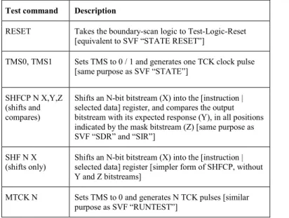
TABLE II. TEST COMMANDS SUPPORTED BY OUR COPROCESSOR.
Test command Description
RESET Takes the boundary-scan logic to Test-Logic-Reset [equivalent to SVF “STATE RESET”]
TMS0, TMS1 Sets TMS to 0 / 1 and generates one TCK clock pulse [same purpose as SVF “STATE”]
SHFCP N X,Y,Z (shifts and compares)
Shifts an N-bit bitstream (X) into the [instruction | selected data] register, and compares the output bitstream with its expected response (Y), in all positions indicated by the mask bitstream (Z) [same purpose as SVF “SDR” and “SIR”]
SHF N X (shifts only)
Shifts an N-bit bitstream (X) into the [instruction | selected data] register [simpler form of SHFCP, without Y and Z bitstreams]
MTCK N Sets TMS to 0 and generates N TCK pulses [similar purpose as SVF “RUNTEST”]
To address these shortcomings, our proposed test coprocessor offers a straightforward way of expanding the test command set. In order to cope with existing and anticipated requirements of test program generation for IEEE 1149.x-compliant boards, the architecture described in this paper supports the simple IEEE 1149.1 instruction set core that is represented in table II.
III. CONTROL PATH AND COPROCESSOR ARCHITECTURE
Any formal representation of the functionality of the commands shown in table II assumes a given hardware architecture, bringing into evidence the corresponding control and data flow operations. The latter will determine the blocks required in the coprocessor data path, which will be implemented with regular sequential circuits. There is a higher degree of freedom in what concerns the implementation of the control path, which can be hardwired or microprogrammed, and the formal representation of each test command will be influenced by the decision of implementing the control path as either a Moore or Mealy state machine. The former will only update its outputs (the control signals to the data path) upon the rising edge of the system clock, while the latter can update its outputs at any moment.
Figure 2 shows an excerpt of an ASMD chart that can be used to represent the behavior of the SHF test command. States 2 and 3 in figure 2 include conditional output boxes used to define Mealy outputs that depend on the condition indicated in the preceding decision box. On the other hand, states 2, 4 and 5 comprise non-empty state boxes used to define Moore outputs, which will be asserted while the controller remains in the corresponding state. Notice that:
⋅ State 2 contains two Moore assignments (load serializer and read FIFO), has two decision boxes, and three Mealy outputs ⋅ State 3 asserts no Moore outputs, has a single decision box,
and two Mealy outputs
⋅ States 4 and 5 assert Moore outputs, and have no decision boxes / conditional outputs
978-1-4799-5743-9/14/$31.00 ©2014 IEEE
The representation in figure 2 can also be used to estimatethe execution speed, by considering the time required to move from state 2 to state 4, assuming that 1) conditions B and C hold true, and 2) condition D holds false for five times. The corresponding state transition will therefore be 2-3-5-3-5-3-5-3-5-3-5-3-4, requiring a total of 12 clock cycles.
The implementation of the same functional behavior as a Moore machine will increase the number of states, since each conditional output box will have to be converted into an equivalent state box, generating a corresponding extra state. The formal representation of the same ASMD chart, converted to a Moore machine, is shown in figure 3. This conversion increases the number of states by a factor of 2.25 (from 4 to 9), but does not cause a proportional degradation of cost or performance, be it in number of logic gates or microprogram memory positions (spatial resources), or in number of clock cycles (speed). Considering the same initial and final states, and the same assumptions as indicated for the Mealy case, the equivalent transition will go through states 2-3-8-5-9-5-9-5-9-5-9-5-9-5-6-7, and require a total of 15 clock cycles (only 1.25 times more than the corresponding Mealy representation).
In order to compare the corresponding implementations in terms of logic resources, a choice will have to be made between a hardwired or a microprogrammed control path architecture. Our choice of a microprogrammed architecture is due to two main reasons: 1) A hardwired controller needs to be completely redesigned when a new test command is required, and the designer will have to build the HDL code for each new ASMD chart. 2) Even if major differences are not to be expected, a hardwired architecture will correspond to a new sum-of-products (or a similar canonical form) for each set of test commands, meaning that there will be variations in the critical path and maximum propagation delay.
Fig. 3. Partial representation of the SHF command as a Moore machine.
The basic control path architecture for a microprogrammed implementation is shown in figure 4 (adapted from [10]). In this case, the most significant address bits of the microprogram memory are determined by the test command opcode (loaded into the Bank_reg latch), and the ASMD state encoding defines the least significant address bits. This architecture is best in terms of simplicity, and enables a very straightforward implementation of any test command – each state in the ASMD chart will correspond to one word in the microprogram memory, and the operation flow can simply be specified as a sequence of “Continue”, “Jump” or “Branch if” microinstructions, directing the state transition from beginning to end. However, it can only implement Moore machines, since each ASMD state selects a single microprogram memory position. Since the ASMD blocks frequently contain conditional output boxes, or more than one decision box, there is a need for preprocessing the ASMD chart, in order to ensure a pure Moore behavior. The total number of states increases, and so does the number of microprogram memory positions, as well as the number of system clock cycles needed to complete the execution of the corresponding test command (one clock cycle per ASMD chart state).
Fig. 4. Basic microprogrammed architecture for a Moore control path [9].
The general rule for preprocessing the ASMD charts consists of eliminating all conditional output boxes, and splitting the states when more than one decision box is present. In addition, and since the most significant bits come directly from the test command opcode, the number of microprogram memory positions used to implement each command is fixed. There is a waste of FPGA floorspace, since the most complex command, with the longest ASMD chart representation, will dictate the number of positions that will be used for all other commands. The control path architecture of figure 4 is able to implement any Moore ASMD chart, and would take 9 memory positions to represent the example represented in figure 3. If this was the highest number of states in any command, we would need 4 least significant bits, meaning that the total storage requirements would be given by 24*O = 16*O, where O is the number of opcodes comprised in the test command set.
If we want to enable the implementation of Mealy behaviors, the microprogram memory least significant bits will have to be driven directly from data path conditions. The main drawback of this solution is that the number of microprogram
978-1-4799-5743-9/14/$31.00 ©2014 IEEE
memory positions will be equal to S*2D, where S is the numberof states, and D is the maximum number of decision boxes existing in a single state (16 memory positions for the example illustrated in figure 2). For a test command set with O opcodes, we would have a total microprogram memory storage requirement given by S*2D*O. While this modification means that we will now have two (or a power of two) microprogram memory positions for each ASMD chart state, the end result is not necessarily an explosion of the microprogram memory space, particularly if state decomposition follows the rule of preventing multiple decision boxes per ASMD state.
A Mealy architecture enables the fastest implementation, but is the most expensive in terms of microprogram memory storage. The intermediate simple Mealy solution limited to one decision box per state is likewise an intermediate solution in terms of speed vs. microprogram memory storage, while the simple Moore representation is cheapest in terms of microprogram memory storage. It is also the slowest, although the number of clock cycles is not proportional to the number of states (being dictated by the path through the ASMD chart).
An improved solution, although with the same execution speed of the basic Moore architecture, is represented in figure 5, and was used to implement the control path of our test coprocessor. Its main advantage over the basic Mealy and basic Moore architectures consists of eliminating the waste of memory positions, since the microcode storage requirements are in this case limited to the number of states in the ASMD chart (instead of the being fixed, and dictated by the chart with the highest number of states).
Fig. 5. Improved microprogrammed architecture for Moore machines.
Table III summarises the pros and cons of three alternatives: Moore (no conditional outputs allowed, maximum state decomposition), Mealy 1 (one decision box and its corresponding conditional output boxes per state), and Mealy 2 (up to two decision boxes and four conditional output boxes).
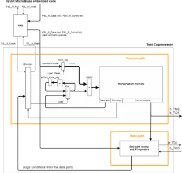
The specific nature of scan test infrastructures dictates that the number of required micro-operations is very small, and accordingly the data path architecture will have a small number of elements, comprising counters, latches and serializers. The conditions associated with these data path elements consist essentially of detecting if the latches and counters reached one or zero. Our microprogrammed test coprocessor architecture is illustrated in figure 6.
TABLE III. PROS AND CONS OF MOORE, MEALY-1, AND MEALY-2
MICROPROGRAMMED CONTROL PATH IMPLEMENTATIONS.
Topology Pros Cons Comments
Moore Maximum simplicity
Lowest speed Preprocessing required
Mealy 1 Good speed upgrade Higher number of memory positions Minimum preprocessing Mealy 2 Marginal speed upgrade over Mealy 1 Highest number of memory positions, many unused No preprocessing (if the number of decision boxes per state is ≤ 2)
The data path needed to support the simplest shift operations requires basically two main types of blocks – counters to keep track of the number of clock cycles required, and serializers, both for converting the parallel words coming from the MicroBlaze into the serial bitstreams that feed the board TDI (b_TDI), and also for feeding the comparator that checks if each bit coming from the board TDO (b_TDO) matches its expected value.
Fig. 6. The proposed test coprocessor architecture and interface method.
IV. TEST COMMAND DESIGN
The microprogrammed control path illustrated in figure 5 is able to implement the control flow associated with any ASMD chart that is specified in the form of a Moore machine. Each state in the chart corresponds to one microprogram memory position, which comprises the following three fields:
⋅ The leftmost bits represent the new address, to be used with the JUMP micro-operation. The number of bits in this field is
dictated by the maximum number of states in the ASMD chart of a single test command.
⋅ The middle field contains the micro-operation that represents the required control flow. The implementation of
978-1-4799-5743-9/14/$31.00 ©2014 IEEE
any ASMD chart requires three types of micro-operations: 1)CONTINUE (increment the current microprogram memory
address); 2) JUMP TO ADDRESS (load the “new address”); and
3) BRANCH IF CONDITION TO ADDRESS (jump to the indicated address if the condition is true, or continue to the next address otherwise). This third type generates a variety of different micro-operations, i.e. BRANCH IF Condition_A is formally different from BRANCH IF /Condition_A (branch if
not condition). The number of bits in this field is determined by 2 (CONTINUE, JUMP) plus the total number of “Branch if”
micro-operations required.
⋅ The rightmost field comprises all the control bits that determine the data flow operations. In our horizontal microprogrammed architecture, the number of bits in this field is equal to the total number of control bits required by the data path elements, plus the additional bits driving TAP pins (board TMS and board TCK).
Expanding our test command set can be done by a simple sequence comprising the following steps:
1. Draw the ASMD chart specifying the operation of the required test command
2. If the ASMD chart contains conditional output boxes (Mealy machine), split those states to convert all conditional output boxes into state boxes (convert from Mealy to Moore). 3. Once the Moore ASMD chart is available, fill in the
microprogram memory template with the micro-operations and control bit patterns corresponding to each ASMD state. 4. Update the content of the microprogram memory.
Fig. 7. MTCK ASMD chart (Mealy representation).
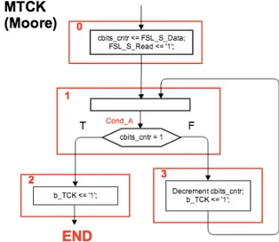
As an illustrative example, figure 7 shows an ASMD chart for the MTCK N test command, which is used for various types of built-in self-test functions (e.g. those that rely on pseudo-random pattern generation and parallel signature analysis modes). The MTCK command starts by loading the number of required b_TCK pulses (present in the FSL_S_Data bus) into one of the data path counters (cbits_cntr in this example), which will be decremented for each b_TCK pulse generated. State 1 requires two microprogram memory positions, since the decrement control signal for cbits_cntr may, or may not, be active in this state. Figure 8 represents the equivalent Moore
ASMD chart, and shows that splitting a state, in order to ensure that a conditional output box is converted into a corresponding state box, does not necessarily increase the number of states in the ASMD chart.
Fig. 8. MTCK ASMD chart (Moore representation).
Each state in the ASMD chart represented in figure 8 now corresponds to a single microprogram memory position, and we are ready to move into the third test command design step, where the microprogram memory template is filled to represent all control and data flow operations associated to MTCK. Table IV shows the content of the four microprogram memory positions that are needed to specify the execution of MTCK.
TABLE IV. CONTENT OF THE MICROPROGRAM MEMORY FOR MTCK.
Pos. New address Micro-operation
0 X CONT
1 Offset to “3” BIF /A
2 Offset to “END” JUMP
3 Offset to “1” JUMP
Pos. iwL iwD rbL cbL cbD cbM sL sS bTMS bTCK
0 0 0 0 1 0 0 0 0 0 0
1 0 0 0 0 0 0 0 0 0 0
2 0 0 0 0 0 0 0 0 0 1
3 0 0 0 0 1 0 0 0 0 1
V. PERFORMANCE AND LOGIC RESOURCE USAGE
The architecture represented in figure 6 was implemented in a Spartan 6 FPGA, using a Digilent Nexys™3 board, and Xilinx’s ISE Design Suite System Edition. The logic resources used and timing performance data are shown in tables V and VI. The rationale behind the collection of the data shown in these two tables can be summarised as follows:
⋅ The columns showing data for each test command (the four rightmost columns) correspond to the implementation of a single command, without the FSL interface
⋅ Since the FSL interface is predesigned and independent of the proposed microprogrammed architecture, tables V and VI include two columns showing the implementation data for all commands when no FSL interface is present, and when one 5-word 32-bit FIFO FSL interface is added (from the MicroBlaze to the test coprocessor)
978-1-4799-5743-9/14/$31.00 ©2014 IEEE
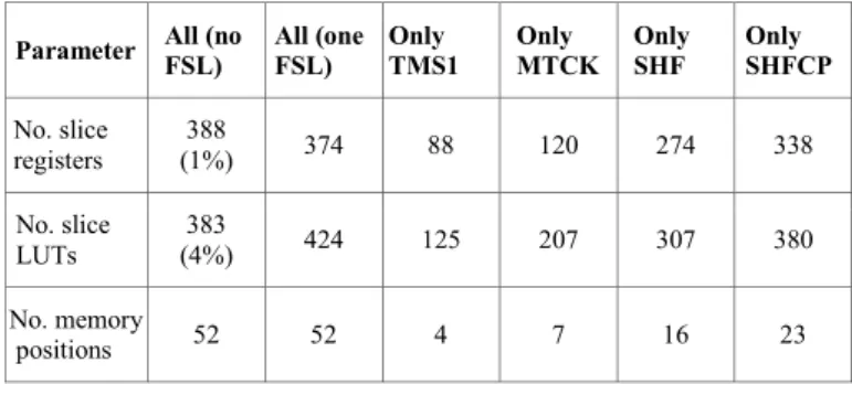
TABLE V. LOGIC RESOURCE USAGE.Parameter All (no FSL) All (one FSL) Only TMS1 Only MTCK Only SHF Only SHFCP
No. slice registers 388 (1%) 374 88 120 274 338 No. slice LUTs 383 (4%) 424 125 207 307 380 No. memory positions 52 52 4 7 16 23
TABLE VI. TIMING PERFORMANCE.
Parameter All (no FSL) All (one FSL) Only TMS1 Only MTCK Only SHF Only SHFCP Min. period / Max. freq. 12.276 ns / 81.457 MHz 12.315 ns / 81.199 MHz 6.053 ns / 165.211 MHz 6.249 ns / 160.037 MHz 7.722 ns / 128.662 MHz 11.246 ns / 88.917 MHz Max. comb. path delay 5.157 ns 8.102 ns 5.157 ns 5.385 ns 5.385 ns 5.519 ns
TMS1 and TMS0 belong to the same group of results, and the same happens with MTCK and RESET, so each second command was omitted in tables V and VI to improve readability. It is important to notice that the usage of logic resources imposed by the most complex test command (SHFCP) dictates the cost of the full implementation – the sole implementation of SHFCP requires practically the same resources as the full implementation of all the test commands presented in table II. The number of microprogram memory positions when the full set of test commands is implemented (52 in total) can be calculated by adding the equivalent value for each command individually, but taking into account that the two first positions are common to all test commands.
In what concerns timing performance, we again notice that the most complex command is the main contributor to determine the minimum period / maximum frequency of operation, although in this case the full implementation is circa 30% slower than what would correspond to SHFCP alone. The minimum period is very close to the maximum combinational path delay, in the case of the sole implementation of test commands TMS1, TMS0, MTCK, or RESET, but is less so as we move into the more complex test commands (SHF and SHFCP).
VI. CONCLUSION
Several IEEE 1149.1 test controller solutions have been developed over the years [11:12], but little attention has been given to controller architectures proposed as embedded coprocessors. The proposed test coprocessor supports a wide range of online testing applications for embedded systems based on single or multi-core 32-bit MicroBlaze CPUs, from built-in self-test to online fault detection and diagnosis [13].
The simplicity of the architecture presented in figure 6 enables a relatively fast execution of the test command set, which reaches slightly more than 80% of the Nexys™3 board system clock (100 MHz). The use of a microprogrammed control path architecture offers a highly flexible solution, simplifying the expansion of the test command set.
Our current work is now focussed on adding new commands to accommodate IEEE 1149.7 debug and test operations [7], and namely the implementation of advanced scan formats (MScan, OScan and SScan). The development work done so far leads us to believe that the coprocessor architecture represented in figure 7 fully supports the 1149.7 scan operations. Future research plans may consider the expansion of the test command set in order to support embedded instruments and other advanced built-in functions defined in the IEEE P1687 [8].
REFERENCES
[1] IEEE 1149.1-2001 (Revision of IEEE Std 1149.1-1990), IEEE Standard Test Access Port and Boundary-Scan Architecture, IEEE Computer Society (Test Technology Standards Committee), 25 October 2001. [2] Serial Vector Format (SVF) Specification (available on-line at
http://goo.gl/ARFMI1, visited on March 12th 2014).
[3] IEEE Std 1149.6-2003, IEEE Standard for Boundary-Scan Testing of Advanced Digital Networks, IEEE Computer Society (Test Technology Standards Committee), 17 April 2003.
[4] Adam W. Ley, “Doing More with Less -- An IEEE 1149.7 Embedded Tutorial: Standard for Reduced-pin and Enhanced-functionality Test Access Port and Boundary-Scan Architecture”, Proceedings of the IEEE International Test Conference, 2009 (available online at
http://goo.gl/3q6Pzd, visited on 10 March 2014).
[5] Michael Williams, “Low Pin-count Debug Interfaces for Multi-device Systems”, ARM’s Serial Wire Debug white paper, 2009 (available online at http://goo.gl/Fkg5lv, visited on 10 March 2014).
[6] Whetsel. L. (1997). An IEEE 1149.1 based test access architecture for IC with embedded core. In: Test Conference, 1997. Proceedings, International. (Washington, DC Nov 1997).
[7] IEEE 1149.7-2009, IEEE Standard for Reduced-Pin and Enhanced-Functionality Test Access Port and Boundary-Scan Architecture, IEEE Computer Society (Test Technology Standards Committee), 10 February 2010.
[8] IEEE P1687 Draft Standard for Access and Control of Instrumentation Embedded within a Semiconductor Device, IEEE Computer Society (Test Technology Standards Committee).
[9] LogiCORE™ IP FSL V20 Fast Simplex Link (FSL), Xilinx (available online at http://goo.gl/2EyZ6t, visited on 10 March 2014).
[10] Michael A. Lynch, Microprogrammed State Machine Design, CRC Press, 1993, ISBN 0-8493-4464-6.
[11] Yau, C. W.; Jarwala, N. (1990) The Boundary-Scan Master: Target Applications and Functional Requirements. Proceedings of the IEEE International Test Conference, 311-315.
[12] Cabral, C. J. (2012) Design and Implementation of an IEEE 1149.7-Compliant cJTAG Controller for Debug and Trace Probe, Master of Science in Engineering Report, Faculty of the Graduate School of the University of Texas at Austin, 55 pp.
[13] Bernardi.Paolo. (2013) MIHTS: a hardware techniques for embedded microprocessor functional on-line self-test. In: Computers. IEEE Transactions (2013).
![Fig. 4. Basic microprogrammed architecture for a Moore control path [9].](https://thumb-eu.123doks.com/thumbv2/123dok_br/18718207.918351/3.892.85.416.654.1046/fig-basic-microprogrammed-architecture-moore-control-path.webp)