niobate thin films crystallized by conventional furnace and
rapid-thermal annealing process
R.G. Mendes
Universidade Federal de Sa˜o Carlos, Departamento de Fı´sica, Grupo de Ceraˆmicas Ferroele´tricas, Caixa Postal 676, 13565-670 Sa˜o Carlos, SP, Brazil
E.B. Arau´joa)
Universidade Estadual Paulista, Departamento de Fı´sica e Quı´mica, Grupo de Vidros e Ceraˆmicas, Caixa Postal 31, 15385-000 Ilha Solteira, SP, Brazil
J.A. Eiras
Universidade Federal de Sa˜o Carlos, Departamento de Fı´sica, Grupo de Ceraˆmicas Ferroele´tricas, Caixa Postal 676, 13565-670 Sa˜o Carlos, SP, Brazil
(Received 5 September 2000; accepted August 6, 2001)
Strontium barium niobate (SBN) thin films were crystallized by conventional electric furnace annealing and by rapid-thermal annealing (RTA) at different temperatures. The average grain size of films was 70 nm and thickness around 500 nm. Using x-ray diffraction, we identified the presence of polycrystalline SBN phase for films annealed from 500 to 700 °C in both cases. Phases such as SrNb2O6 and BaNb2O6 were
predominantly crystallized in films annealed at 500 °C, disappearing at higher temperatures. Dielectric and ferroelectric parameters obtained from films crystallized by conventional furnace and RTA presented essentially the same values.
I. INTRODUCTION
The tungsten bronze family is one of several ferroelec-tric materials. Since 1949, when the tungsten bronze structure was deduced by Magneli,1numerous tungsten
bronzes have been synthesized. The tungsten bronze family includes niobates such as (Sr,Ba)Nb2O6 (SBN),
(Pb,Ba)Nb2O6 (PBN), and (Pb,K)Nb2O6 (PKN). PBN
and PKN are orthorhombic tungsten bronze structure with a point group mm2. On the other hand, SBN
(SrxBa1−xNb2O6), with 0.25 < x < 0.75, presents a
te-tragonal (4mm) phase at room temperature. A solid
so-lution of SBN exists in the binary SrNb2O6–BaNb2O6
system. Investigations using x-ray diffraction (XRD) suggested a morphotropic phase boundary around x 4
0.25, which is characterized by the coexistence of the tetragonal and orthorhombic phases.2
The excellent ferroelectric and electro-optic properties exhibited by SBN make this material promising for a variety of applications. SBN has received great attention as a ferroelectric material due to its large pyroelectric coefficient,3piezoelectric,4and electro-optic properties.5
In recent years, the development of integrated optical devices has stimulated the demand for thin films using attractive materials such as SBN. SBN thin films have been prepared by several techniques like sol-gel proc-essing,6 pulsed laser deposition,7 and metalorganic
chemical vapor deposition (MOCVD).8 Large-scale
processing of high-quality thin films requires low-temperature synthesis, high reproducibility, simplicity in all processing steps, and low cost. Due to this fact, the search for new routes for film preparation remains an interesting and open subject in order to improve the sta-bility of complex solutions, the control of the stoichi-ometry of the film composition, or to reduce the cost of the process. Very recently, the preparation of SBN thin films by a chemical method based on a polymeric resin containing metallic ions was proposed.9The method was
successfully applied to prepare SBN thin films of good quality and homogeneity.
In this work, SBN thin films obtained by the early cited method were studied under its structural, dielectric, and ferroelectric properties. The effect of the different heat treatments on SBN thin films, using conventional furnace and rapid-thermal annealing (RTA), was studied. Dielectric and ferroelectric properties are presented for films crystallized at different temperatures.
II. EXPERIMENTAL PROCEDURE
In this work SBN films were prepared by a hybrid chemical method used to produce a polymeric resin.9The
general idea is to distribute the metallic ions homoge-neously throughout the polymeric resin, prepared accord-ing to the Pechini method.10 The process calls for
forming a chelate between dissolved ions with a hy-droxycarboxylic acid (citric acid). Heating of the resin in air causes a breakdown of the polymer. Subse-quently, the ions are oxidized to form the desired crystal-line phases.
Barium oxide (BaO), strontium carbonate (SrCO3), and
ammoniac complex [NH4H2NbO(C2O4)?3H2O] were
selected as starting materials. The molar ratio of starting materials was calculated to obtain a final Sr0.75Ba0.25Nb2O6
(SBN 75/25) composition. For preparation of the resin, BaO, SrCO3, and NH4H2NbO(C2O4)?3H2O were
ini-tially dissolved in water to form a transparent solution. Next, each solution was mixed separately with citric acid and heated to 40 °C for 30 min. This stage is im-portant to form chelate between mixed cations with a hydroxycarboxylic acid (citric acid). Then, each solution was mixed with ethylene glycol (citric acid/ethylene glycol 4 50/50) and polymerized by heating up to 100 °C for 30 min. Finally, the three solutions were mixed at room temperature and heated again to 50 °C and stirred during 20 min to homogenization, when a trans-parent resin was obtained. The final transtrans-parent resin indicates that all metallic ions were distributed throughout the polymeric resin.
Films of the resins were deposited at room temperature on Pt/Si substrates by spin coating at 4500 rpm for 40 s. Films were obtained by depositing multiple layers of this resin. Each layer was annealed at 400 °C for 3 h to re-move organic material. The process was repeated for eight deposited layers to obtain a dense film. Deposited films were crack free, uniform, and well adhered on substrates. For crystallization, films deposited on Pt/Si substrates were annealed in a conventional electric fur-nace at 500, 600, and 700 °C for 1 h. The rapid-thermal crystallization was carried out in a Research INC power controller Model 664F RTA furnace at 500, 600, and 700 °C for 60 s. This RTA process permits heating rates between 10 to 50 °C/s.
The structure of the crystallized films at different temperatures was analyzed by XRD using Cu Ka radi-ation at room temperature. The morphological exam-ination of SBN films was performed on a JEOL JSM-5800 (Tokyo, Japan) scanning electron microscope (SEM). The dielectric constant (e) and dissipation factor (tand) were measured from 500- to 500-kHz frequency using an HP 4194A impedance analyzer. A Sawyer-Tower circuit was used to measure the ferroelectric prop-erties at 100 Hz.
III. RESULTS AND DISCUSSION
SBN films of good quality were obtained in this work. Figure 1 shows an SEM photomicrograph of the cross-sectional view of SBN thin film deposited on Pt/Si sub-strate. This film was crystallized at 700 °C for 1 h using a conventional furnace. Based on Fig. 1, measured thick-ness of the film was 500 nm and grain size was around 70 nm, on average.
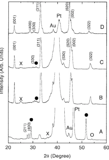
The effect of temperature crystallization in SBN films was investigated under different conditions. Figure 2 shows XRD patterns for SBN films crystallized by con-ventional furnace and RTA process. Peaks identified in this figure were attributed to tetragonal SBN phase. As shown in Fig. 2, polycrystalline SBN phase crystallizes better on films annealed at 600 and 700 °C for 1 h. Some structural fluctuation can be seen for films annealed at 500 °C [Fig. 2(A)] when the well-defined (211) and (400) peaks were observed. These peaks disappear for films crystallized at 600 °C [Fig. 2(B)] and 700 °C [Fig. 2(C)].
Based on XRD patterns, changes of full width at half-maximum (FWHM) for some (hkl) peaks represent the
degree of crystallization as a function of annealing tem-perature. The FWHMs of (311) peak in Fig. 2 were 0.72°, 0.63°, and 0.57° for films respectively annealed at 500, 600, and 700 °C for 1 h. These facts show that when annealing temperature increases the crystallization of SBN films on Pt/Si is improved. In Fig. 2(A) we can also identify the presence of the SrNb2O6 (SN) and
BaNb2O6 (BN) phases for films annealed at 500 °C for
1 h. When temperature increases, BN disappears but SN remains at film annealed at 600 and 700 °C for 1 h. Neither SN nor BN is a ferroelectric material with the tungsten bronze structure. They are components of the solid solution that yields ferroelectric SBN.
Figure 2(D) shows XRD patterns of the SBN films crystallized by RTA at 700 °C for 60 s. The FWHM of the (311) peak was 0.57°, indicating similar behavior of SBN film crystallized by conventional method at same temperature. As observed in Fig. 2(D), SBN was crys-tallized without SN phase and this may be attributed to effective crystallization of the SBN phase using the RTA process. Films were also crystallized at 500 and 600 °C for 60 s using RTA, not shown here. These films pre-sented essentially the same results, in terms of crystalli-zation, as films crystallized in a conventional furnace at the same temperatures.
Based on XRD patterns of SBN films crystallized at 700 °C by conventional and RTA methods, the lattice constants a and c were calculated for tetragonal phase
using the (001), (311), (002), and (322) peaks. For the film annealed by the conventional method, the calculated lattice constants were a 4 11.57 Å and c 4 4.00 Å, whilea411.62 Å andc44.03 Å for film crystallized by RTA. The lattice parameters a and c obtained here
agreed relatively well with results of the literature for SBN 75/25 thin film obtained by MOCVD, whose values are around a 412.430 Å and c43.932 Å.8For bulk crystals with the same composition the lattice parameters are a412.458 Å andc43.928 Å.11
Films annealed at 700 °C by the conventional method (for 1 h) and RTA (for 60 s) were used for dielectric and ferroelectric measurements because these films presented better crystallization. The dielectric behavior of the SBN films, examined in terms of the dielectric constant (e) dissipation factor (tan d) as functions of measuring fre-quency, are summarized in Fig. 3.
It may be seen that dielectric constant exhibits a slight frequency dependency, which is consistent with the ex-pected normal behavior. The dielectric constant and dis-sipation factor at a frequency of 100 kHz were 119 and 0.164, respectively, for film crystallized by the conven-tional method at 700 °C for 1 h. For film crystallized using the RTA method these values were respectively 107 and 0.088. The value of the dielectric constant ob-tained here is consistent with other reports for SBN thin films obtained through metal alkoxide.12 The observed
frequency dispersion at lower frequencies of the dissipa-tion factor (tan d) is probably related to interfacial ef-fects, often denominated the Maxwell–Wagner type.
Hysteresis loops were observed at room temperature, at 100 Hz. Figure 4 shows P-E hysteresis loop of SBN films crystallized by conventional furnace at 700 °C for 1 h and by RTA at 700 °C for 60 s. Rounded curves were found due to the low-frequency high-loss characteristics of the films. The remanent polarization (Pr) and the
co-ercive field (Ec) were 17.8mC/cm2and 180 kV/cm,
re-spectively, for the SBN film annealed in a conventional furnace at 700 °C for 1 h. Similar results were obtained for films crystallized by the RTA method. This film pre-sented Pr 416 mC/cm2 and Ec 4 155 kV/cm. In the literature, reported values of Pr and Ec for SBN 75/25
films ranged from 1.9 to 34mC/cm2and 51 to 180 kV/cm,
FIG. 2. XRD patterns of SBN thin films deposited on Pt/Si substrate. Films were crystallized by conventional furnace at (A) 500 °C, (B) 600 °C, and (C) 700 °C for 1 h and (D) by RTA process at 700 °C for 60 s. Symbols represent (×) unidentified phase, (d) SrNb2O6, and (s)
BaNb2O6.
respectively, obtained by sol-gel.12,13 In this work,
the observed Pr is lower if compared with values
ob-served for crystals, whose values ranged from 27 to 32 mC/cm2.11 However, the coercive field (Ec) and re-manent polarization (Pr) values obtained here for SBN
thin films may not correspond to intrinsic values because the conductivity effect was not discounted in loop hys-teresis of Fig. 4. Thus, the distortion observed on hysteresis is probably associated with the effect of conductivity in SBN films, which may be attributed to the presence of undesirable coexistence of phases on films such as Sr0.75Ba0.25Nb2O6 (SBN 75/25) and
SrNb2O6(SN).
The capacitance–voltage (C–V) characteristic was also studied on films crystallized at 700 °C. A small alternating-current signal of 10-mV amplitude and 100-kHz frequency was applied across the sample while the direct-current electric field was swept from positive
bias to negative bias and back again. Figure 5 shows the C–V characteristic of the film crystallized by the con-ventional furnace; film prepared by RTA presented a similar result. The two maximas, which are due to fer-roelectric polarization reversals, associated with double coercive field (Ec), are clearly seen in Fig. 5. Generally
the coercive field determined by C–V measurements are somewhat smaller than Ecdetermined from the hysteresis
loop measurements due to dependence of Ec on the
ap-plied voltage and frequency. Note that the two peaks are of different height and there is a small offset toward positive bias. Considering a ferroelectric, the polarization and dielectric constant vary nonlinearly with applied field. In some cases, a space charge is formed at inter-faces and, under conditions of reverse bias, a depletion layer forms.14Asymmetry and shift in C–V curve may be
observed if a disparity of the space charge occurs. In general, observed effects are associated with contacts and may be minimized with adequate postannealing of the films.
IV. CONCLUSIONS
Polycrystalline SBN thin films of high density were crystallized on Pt/Si substrates using a polymeric resin. Results showed good crystallization of SBN films, crys-tallized using a conventional furnace or RTA. Undesired phases such as SrNb2O6 and BaNb2O6 appear in films
deposited at 500 °C but these phases disappear at higher temperatures. Finally, dielectric and ferroelectric param-eters presented essentially the same values for films crys-tallized by a conventional furnace and RTA. Thus, for purposes of future applications in microelectronic de-vices, the preparation of SBN films by the RTA method is of interest. In this case, the final product will be less expensive than other SBN thin films produced by other physical methods. The main and distinct advantage over other chemical methods, especially sol-gel, is asso-ciated with the high stability observed in polymeric resin used on film deposition. Previous stability investigations showed that these resins could be used after 1 year with-out appreciable changes in structural, microstructural, and electric characteristics of the films. The next step is to study ideal conditions to eliminate or minimize unde-sirable observed effects in dielectric characteristics of the SBN films.
ACKNOWLEDGMENTS
The authors are grateful to C-N-P-q and F-A-P-E-S-P (processes 98/16513-5 and 99/02485-2) for financial support, to Dr. Yvonne P. Mascarenhas (IFS -C-U-S-P) for XRD facilities, and to Mr. Francisco J. Picon (D-F - U-F-S-C-a-r) for technical support. FIG. 4. Hysteresis loop, measured at 100 Hz, of SBN film annealed by
a conventional furnace at 700 °C for 1 h and RTA at 700 °C for 60 s.
REFERENCES
1. A. Magneli, Ark. Kemi1,213 (1949).
2. S. Nishiwaki, J. Takahashi, K. Kodaira, and M. Kishi, Jpn. J. Appl. Phys.35,5137 (1996).
3. A.M. Glass, J. Appl. Phys.40,4699 (1969).
4. J.D. Zook and S.T. Liu, J. Appl. Phys.49,4604 (1978).
5. M. Horowitz, A. Bekker, and B. Fischer, Appl. Phys. Lett.62,
2619 (1993).
6. Y. Xu, C.J. Chen, R. Xu, and J.D. Mackenzie, Phys. Rev. B44,35
(1991).
7. S.S. Tho¨ny, K.E. Youden, J.S. Harris, Jr., and L. Hesselink, Appl. Phys. Lett.65,2018 (1994).
8. M. Lee and R.S. Feigelson, J. Cryst. Growth180,220 (1997).
9. R.G. Mendes, E.B. Arau´jo, H. Klein, and J.A. Eiras, J. Mater. Sci. Lett.18,1941 (1999).
10. P.A. Lessing, Ceram. Bull.68,1002 (1989).
11. R.R. Neurgaonkar, W.F. Hall, J.R. Oliver, W.W. Ho, and W.K. Cory, Ferroelectrics87,167 (1988).
12. W. Sakamoto, T. Yogo, K. Kikuta, K. Ogiso, A. Kawase, and S. Hirano, J. Am. Ceram. Soc.79,2283 (1996).
13. C.J. Chen, Y. Xu, R. Xu, and J.D. Mackenzie, J. Appl. Phys.69,
1763 (1991).
14. J.M. Bell, P.C. Knight, and G.R. Johnston, inFerroelectric Thin Films: Synthesis and Basic Properties,edited by C. Paz de Araujo,