Correspondence to:T. Ott ([email protected])
Received: 17 September 2015 – Accepted: 12 October 2015 – Published: 13 November 2015
Abstract. Sensitive and selective gas measurements are crucial for a large variety of applications, e.g., explosion protection. Optical gas detection is usually based on the gas’ absorption of infrared radiation (IR). It is the leading technique in terms of accuracy, reliability, and economic efficiency. Since most gas measurements are made in the two wavelength ranges of (3. . .5) and (8. . .14) µm, a broadband IR source is necessary. In this paper, we report on a novel thermal IR emitter with high radiant power and a near-blackbody emission characteristic that can be modulated electrically. The layout of the IR source had been optimized by use of finite element analyses (FEA) in order to get an adequate electrical resistance as well as a homogeneous temperature distribution and a minimum deflection of the radiating element. Due to its excellent thermal isolation from the heat sink, the electrical power consumption is very low. Operating temperatures of up to 1400 K are possible, so that the fabricated IR source features a very high radiant power. Its application in gas analysis will improve the performance and efficiency of gas measurement systems.
1 Introduction
Explosion hazards mostly arise from flammable gases and vapors. Instead of avoiding their ignition by explosion pro-tection measurements, it may be preferable to detect them before they become ignitable. Depending on the application, different measuring principles for the detection of gases and vapors can be used, e.g., electrochemical sensors (Bakker, 2004), semiconductor sensors (Capone et al., 2004), and point or open-path infrared gas detectors (Goode et al., 1999). Optical gas detection by use of infrared radiation (IR) is the leading technique in terms of accuracy, reliability, and economic efficiency. Since most gas measurements are made in the two wavelength ranges of (3. . .5) and (8. . .14) µm, a broadband IR source with a near-blackbody emission charac-teristic is necessary. For reliable measurements, the genera-tion of a stable spectrum of infrared radiagenera-tion is crucial. Very low detection limits can be realized by a long optical path, where more gas molecules are involved in the IR absorp-tion, but this requires a very powerful IR source. According to Planck’s law of thermal radiation, the spectrum of a ther-mal emitter with a blackbody characteristic depends only on its temperatureT (Howell et al., 2010). The totally emitted radiant powerPSis given by the Stefan–Boltzmann law
PS=εσ AemitT4 (1)
with emissivityε, Stefan–Boltzmann constantσ, and the ra-diating areaAemit. Consequently, a high radiation power is mainly realized by a high operating temperature of the ther-mal emitter, but also by a high and wavelength-independent emissivity of infrared radiation. Especially portable gas sens-ing devices require a low energy consumption of the IR source. For this reason, the radiating element has to be op-timized regarding an excellent thermal isolation.
2 Design and technology
In Schossig et al. (2010) and Schossig (2012), we reported on a novel IR absorber based on a nanostructured NiCr alloy that features a very high and spectrally homogeneous absorp-tivity. From Kirchhoff’s law (Howell et al., 2010),
α(λ, T)=ε(λ, T), (2)
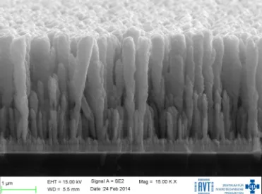
Figure 1.SEM (scanning electron microscopy) picture of a nanos-tructured NiCr absorber.
good emitters. Since NiCr is one of the most used materials in heating elements, for instance in toasters and hairdryers, we studied the application of the nanostructured NiCr ab-sorber (Fig. 1) in thermal infrared emitters to increase their emittance. By depositing the nanostructured NiCr layer on a thin NiCr foil, the high-temperature stability of the nanos-tructures could be verified with a first prototype of a thermal IR emitter in a TO-39 package (Fig. 2). Thereby, operation in air causes an oxidation of the surface. The speed of oxidation and the thickness of the oxide are increased with increasing temperature. As a consequence, the spectral emissivity of the nanostructured surface is affected. In contrast, an operation in an inert gas atmosphere does not change its optical prop-erties even at very high temperatures. The layout of the first prototype had some disadvantages. First, it had a very low electrical resistance of about 1, which is not practicable to use. In addition, the temperature distribution was not homo-geneous, as can be seen from Fig. 2. Finally, it had a rela-tively high power consumption of about 5 W due to the poor thermal isolation of the radiating element.
3 Layout of an ideal heating conductor
As already mentioned, an ideal thermal emitter should fea-ture a high electrical resistance and a low heat capacity (also referred to as thermal mass) in order to be modulated electri-cally. Furthermore, most of the electrical input power should be transformed into radiant power. This can be achieved by a good thermal isolation, a high emissivity near 100 % and a high average temperature of the emitting area. The emis-sivity and the average temperature, however, do not have any effect on the shape of the heating conductor. So the focus is on improving thermal isolation and electrical resistance. A simplified current-carrying heating conductor is shown in
Figure 2.First prototype of a thermal infrared emitter with a nanos-tructured high-emissivity layer operating at about 1170 K.
A emit
ρ
U
PS
d
l
T,ε,̺el,cv
b TU
Aemit
AQ
Figure 3.Physical dimensions and boundary conditions of a sim-plified heating conductor.
Fig. 3. In order to improve its geometric shape, the theoreti-cal dependencies need to be considered.
The electrical resistanceRof a rectangular conductor is
R=̺el l AQ
=̺el l
b d, (3)
where̺elis the specific electrical resistance of the conduc-tor material andlis the conductor length. The cross section AQis the product of conductor thicknessd and its widthb. As given by Eq. (1), the radiant power is proportional to the emitting areaAemit; thus,
Aemit=b l (4)
should be maximized. The conductor material is NiCr. To achieve a high resistance and maximize the emitting area cor-responding to Eqs. (3) and (4), the conductor layout can be optimized as follows.
1. Choose conductor lengthlas large as possible.
Figure 4.Input power and dissipated heat fluxes of the emitter in the TO-39 housing. For simplification, convection is neglected.
Further requirements for thermal emitters are a high mod-ulation depth mf (see Sect. 5 for further explanation) and low thermal losses, which can be described with thermal con-ductance. The thermal conductanceGλis proportional to the conductor’s cross section (Baehr and Stephan, 2011, p. 6):
Gλ∝AQ. (5)
The modulation depth is defined here by the ratio of the achievable temperature difference under electrical modula-tion with frequencyfmvs. the maximum temperature differ-ence without modulation at approximately direct current
mf = 1T(fm)
1T(fm→0)
. (6)
Due to its thermal inertia, the heating conductor requires a certain amount of time to reach the equilibrium tempera-ture after it is turned on. If the modulation frequency is too high, the emitter is not able to reach its equilibrium tempera-ture any more. Thus, the temperatempera-ture difference1T(fm) and therefore modulation depth mf decrease.
The thermal model by Schulz et al. (2005) is used to under-stand the dynamic heating and cooling of the emitter under cyclic excitation. The model describes these thermodynamic processes analytically. Figure 4 shows the heating conductor in the TO-39 housing. The input power Pel is transformed completely into Joule heat. This heat is dissipated into the environment through
– radiationPS,
– solid-state heat conduction within the heating conductor
(Q˙λ,Solid) and the header pins (Q˙λ,Pin), as well as
– heat conduction (Q˙λ,Gas) through the filling gas.
These dissipated heat fluxes will be collectively referred to as Q˙diss subsequently. To describe the thermodynamic be-havior of the arrangement, the heat capacityCthneeds to be
1T =T−TU. (9)
By inserting Eq. 8 into Eq. 7, the rewritten balance equation results:
d1T dt =
Pel− ˙Qdiss Cth
. (10)
If the dissipated heat flux and the input power are not mod-ified, the heating and cooling speed is faster the lower the heat capacity of the conductor is. In consequence, the reduc-tion of the heat capacityCthincreases the modulation depth:
Cth↓⇒mf ↑. (11)
The conductor’s heat capacityCthis given by
Cth=l b d cv, (12)
wherecvis the volume-specific heat capacity.
Considering the given objective on modulation depth and thermal losses, the following conclusions result.
– To ensure a low thermal conductance for a given con-ductor’s widthb, the element thicknessd should be as small as possible.
– A small element thickness beneficially leads to a low thermal mass.
In conclusion, a low element thickness yields to high electri-cal resistance, high modulation depth and low thermal losses. The emitting area is maximized by increasing the conduc-tor’s length and width. Regarding the layout, an ideal heating conductor is as thin, as long and as wide as possible. In con-sequence we choose a thin and long spiral to come as close as possible to an ideal conductor shape.
4 Finite element analysis of heating conductors
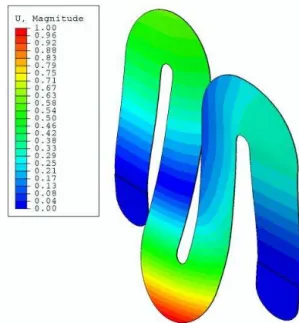
Figure 5.Temperature distribution of(a)meander-shaped and(b)spiral-shaped emitters.
the mean element temperature directly affects the emitted ra-diant power. So temperature should be evenly distributed, leading to a high mean temperature. To assess these char-acteristics, finite element analyses (FEA) have been carried out. The goal is to compare meander-shaped (Fig. 5a) and spiral-shaped conductors (Fig. 5b) with respect to electrical resistance, temperature distribution and out-of-plane deflec-tion (called displacement in FEA).
The boundary conditions for the FEA are the following.
– Thermal: heat sink with TU=20◦C at the pins of the TO39 header;
– electrical: voltageUat the pins;
– optical: emissivity εtop=0.9 of the top surface (with NiCr nanostructures) and εbottom=0.3 of the bottom surface (blank metal); and
– mechanical: fixed support at TO39 pins.
NiCr is used as material. As already mentioned, it can be assumed that all of the electrical input power is transformed into Joule heat.
Table 1 shows the results of the analyses. The temperature distribution of the meander-shaped emitter (Fig. 5a) repro-duces the visual appearance shown in Fig. 2, where hotter ar-eas are brighter. Compared to the meander shape, the spiral-shaped element has far more electrical resistance as well as a uniform temperature distribution (Fig. 5b). This leads to a higher mean temperature of the spiral, although the max-imum element temperatures of both layouts are equal. Due to the higher mean temperature, the spiral-shaped conductor is twice as efficient as the meander-shaped conductor regard-ing emitted radiant power. The fixed support of the conductor ends forces the elements to buckle under thermal load. Fig. 6 shows the meander displacement as a result of buckling. Af-ter a longer period in operation, we discovered malfunction of the emitter caused by buckling (Fig. 7), which is not toler-able. The magnitude of the spiral displacement is much lower (u<0.3 mm), and tolerable.
Figure 6.Displacement (deflection) of the meander in mm.
5 Experimental results
Calculated withPS= εtop+εbottom σ AemitT whereεtop=0.9andεbottom=0.3.
Figure 7. Malfunction of the meander-shaped emitter caused by buckling.
0 5 10 15 20
0.0 0.1 0.2 0.3 0.4 0.5 0.6 0.7 0.8 0.9 1.0
Wavelengthλin➭m
Emissivit
y
Figure 8. Measured spectral emissivity of the novel thermal in-frared emitters with spiral filament.
radiation, a reflector is integrated into the TO-39 housing. In this way, a 70 % higher signal was achieved.
The electrical and optical properties of the new prototypes were studied. We found an adequate electrical cold resis-tance of about 31±3and a slightly higher hot resistance of about 33±3(Fig. 10). Accordingly, the emitters can
Figure 9.Prototype of a thermal infrared emitter with the near-blackbody emission characteristic in TO-39 housing.
be operated at 3.3 V, a common voltage used in portable de-vices. In this case, the mean electrical power consumption is 330 mW±20 mW, with an operating temperature of 970 K (Fig. 11). For temperature measurement the spectral radi-ance has been measured with a monochromator as can be seen in Fig. 13. Then the maximum of the spectral radiance has been determined and converted into a temperature with Wien’s displacement law. The temperature error is estimated at±30 K. Comparable thin-film emitters reach only a maxi-mum temperature of about 800 K at the same electrical input power (Micro-Hybrid Electronic GmbH, p. 5).
0.5 1.0 1.5 2.0 2.5 3.0 3.5 0 20 40 60 80 100 120
VoltageUin V
Curren t I in mA S0803 S0908 S0828 S0830 S0871
Figure 10.Measured current-voltage characteristic of the IR emit-ter from Fig. 9.
100 150 200 250 300 350
300 400 500 600 700
PowerPelin mW
T emp er ature T in ◦C 573 673 773 873 973 T emp er ature T in K
Figure 11.Measured operating temperature in dependence on the electrical power for the IR emitter from Fig. 9.
flux is called normalized optical emission (NOE):
NOE= 18(fm)
18(fm→0)
. (13)
With increasing frequency, NOE decreases due to the thermal inertia of the emitter. Consequently, the frequency response has a low-pass characteristic (Fig. 12). The measurement re-sults show a maximum modulation frequency of about 3 Hz for 50 % NOE. This is sufficient for most applications. How-ever, the NOE and the modulation depth can be simply in-creased by a further reduction of the thermal mass.
Finally, the measurement results of the spectral radiance validate the near-blackbody emission characteristic of this thermal infrared source (Fig. 13).
6 Conclusion and outlook
In this paper, we presented a novel thermal IR emitter for ap-plication in optical gas detection. It features a very high ra-diant power, near-blackbody emission characteristic and can be modulated electrically. Due the excellent thermal isola-tion from the heat sink, the electrical power consumpisola-tion is very low. This enables an application in portable gas sens-ing devices. Since the used NiCr alloy allows a permanent
0.1 1 10
0.1 1
Frequencyfmin Hz
Norm.
optical
emission
(NOE)
3 V, Krypton
Figure 12.Measured frequency response of the emitter for a con-stant voltage square-wave drive.
0 1 2 3 4 5 6 7 8 9 10 11 12 13 14 15
0.01
0.1 1
Wavelengthλin➭m
Norm.
sp
ectral
radiance
Planck (900 K)
S0871 (3 V,295 mW,ZnSe)
S0830 (3 V,288 mW,CaF2)
Figure 13.Comparison of the measured spectral radiance of the novel IR source and a blackbody radiator of the same temperature.
operation at temperatures of up to 1400 K, the fabricated IR source should feature a long-term stable performance and a long lifetime. Finally, its application in gas analysis will im-prove the performance and efficiency of gas measurement systems. Further improvements will target the reduction of the thermal mass of the radiating element in order to increase its modulation depth.
Acknowledgements. The authors would like to thank the German Research Foundation (DFG) for supporting this work under grant number GE 779/32.
Edited by: W. A. Minkina
Goode, J. G., Yokelson, R. J., Susott, R. A., and Ward, D. E.: Trace gas emissions from laboratory biomass fires measured by open-path Fourier transform infrared spectroscopy: Fires in grass and surface fuels, J. Geophys. Res.-Atmos., 104, 21237–21245, doi:10.1029/1999JD900360, 1999.
Howell, J. R., Siegel, R., and Menguc, M. P.: Thermal Radiation Heat Transfer, CRC press Taylor & Francis, 5th edn., Boca Ra-ton, p. 61, doi:10.1002/zamm.201290025, 2010.