High Frequency Performance of GaN
Based IMPATT Diodes
B. Chakrabarti
Department of ECE, Bengal Institute of Technology, Kolkata-150, India
D. Ghosh
Department of ECE, Swami Vivekananda Institute of Science and Technology, Kolkata-145
India [email protected]
M. Mitra
Dept. of E&TC Engg., BESU, Shibpur, Howrah 711103, W.B., India
Abstract:
IMPATT is a p+n junction diode reversed bias to breakdown and can generate microwave power when properly embedded in a resonant cavity. Till emergence on 1965 day by day it became more powerful solid state source for microwave as well as mm-wave frequency range. To get higher efficiency and power output different structures like SDR, DDR, DAR, lo-high-lo, etc. were proposed and developed by different scientists over the years. Then the IMPATT development started with different semiconductor materials like GaAs, InP, GaN, etc. along with Silicon to achieve higher efficiency, power output and frequency range. In this paper the performance of GaN based SDR IMPATT have thoroughly studied in terms of (i) electric field profile[E(x)] (ii) normalized current density profile [P(x)] (iii) Susceptance Vs Conductance characteristics (iv)RF power output (v) negative resistivity profile [R(x)] of the diodes through simulation scheme. It is being observed that the efficiency is 17.9% at Ka-band and because of the very high breakdown voltage, power output is as high as 1.56W in comparison with other frequency band of operations.
Key words: mm wave IMPATT, GaN IMPATT, Ka-band IMPATT oscillator, simulation of IMPATT
1. Introduction:
Over the years it is being found that IMPact Avalanche Transit Time (IMPATT) diodes became most powerful solid state sources in the mm-wave and sub-mm wave frequencies. These devices are now used as transmitter in radars, as a source in the missile seeker head and in many others mm-wave civilian and military applications [Trew et. al. 2005], which includes communication.
dielectric constant determines the device impedance and band gap determines the upper temperature limit for the safe operation of the device. As it can be seen from the Table: 1 that wide band gap semiconductor material such as GaN have (i) seven times higher Ec and (ii) two times higher Vs in comparison to those of Si and GaAs. Also
review works on wide band gap semiconductor establishes the superiority of GaN based high power and high frequency devices [Okumura et. al., 2006]. Overall it is found that high quality GaN films can be grown easily on SiC substrates by MOCVD [Inoki et. al.2003].
The two common types of GaN are, Wurtzite and Zinc-blend .Wurtzite phase (Wz) GaN based IMPATTs have found to perform better than Zinc-blend (ZnB) GaN, in terms of breakdown voltage, efficiency and power output at around 140 GHz [Panda et. al. 2001]. At the same time detail analysis on the dc and small signal properties of GaN (Wz) based IMPATT diodes and there comparative studies have not been reported so far in recent literatures. The authors have taken SDR (p+nn+) (fig:1) structure of GaN IMPATT diode to simulate the dc and small signal behaviors for optimized operation at different mm-wave window frequency bands. The device dimensions, doping and current densities of the diodes (Wz-GaN) are also optimized for Ka, V and W band frequencies after a detailed computer analysis. Then for a known area of the diode and negative conductance, using the procedure described in literature [Eisele et. al. 1997] the RF power generated from the device was simulated.
The analysis of this paper will be extremely helpful for the design of high power, high frequency GaN (Wz) based IMPATT diodes.
2. Material parameters and simulation method:
For the present analysis, a flat profile SDR (n+np+) structure is considered (figure:1), where n+ and p+ are highly doped substrates and top layer respectively, and n is the epi-layer. Experimental values of carrier ionization rates [Electronic Archieve, 2011], Monte Carlo simulated temperature dependent (300k<T<600k) values of drift velocity and mobility of charge carriers in hexagonal (Wz) GaN are considered for the simulation work [Mukherjee et. al, 2007 & Kunihiro et. al. 1999]. All the material parameters values which have been considered for simulation are summarized in table1.
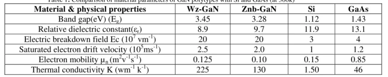
Table 1: Comparison of material parameters of GaN polytypes with Si and GaAs (at 300k)
Material & physical properties Wz-GaN Znb-GaN Si GaAs
Band gap(eV) (Eg) 3.45 3.28 1.12 1.43
Relative dielectric constant(εr) 8.9 9.7 11.9 13.1
Electric breakdown field Ec (107 vm-1) 20 20 3 4
Saturated electron drift velocity (105ms-1) 2.5 2.0 1 1.2
Electron mobility µn (m2v-1s-1) 0.125 0.10 0.15 0.85
Thermal conductivity K (wm-1 k-1) 225 130 1.50 46
2.1 DC Analysis
The static characteristics, such as electric field profile and normalized current density profile of the designed diode are obtained following the D.C method [Mukherjee et. al, 2007]. In the dc method, the numerical computation starts from the field maxima near the metallurgical junction. The distribution of dc electric field and carrier currents in the depletion layer are obtained by a double-iterative simulation method, which involves iteration over the magnitude of field maximum (Em) and its location in the depletion layer. At each point in the
depletion layer simultaneous solutions of Poisson and carrier continuity equations are used. The field boundary conditions are given by,
E(-x1)=0 and E(+x2)=0 (1)
Here –x1 and x2 represent the edges of the depletion layer in n+ and p+ regions, respectively.
The boundary conditions for normalized current density P(x), are given by,
P(-x1)=(2/Mp - 1) and P(x2)=(1 – 2/Mn) (2)
where, Mn = J/Jns, Mp = J/Jps; Jns and Jps are electron and hole leakage current densities, respectively.
Mn and Mp are hole and electron current multiplication factors, respectively.
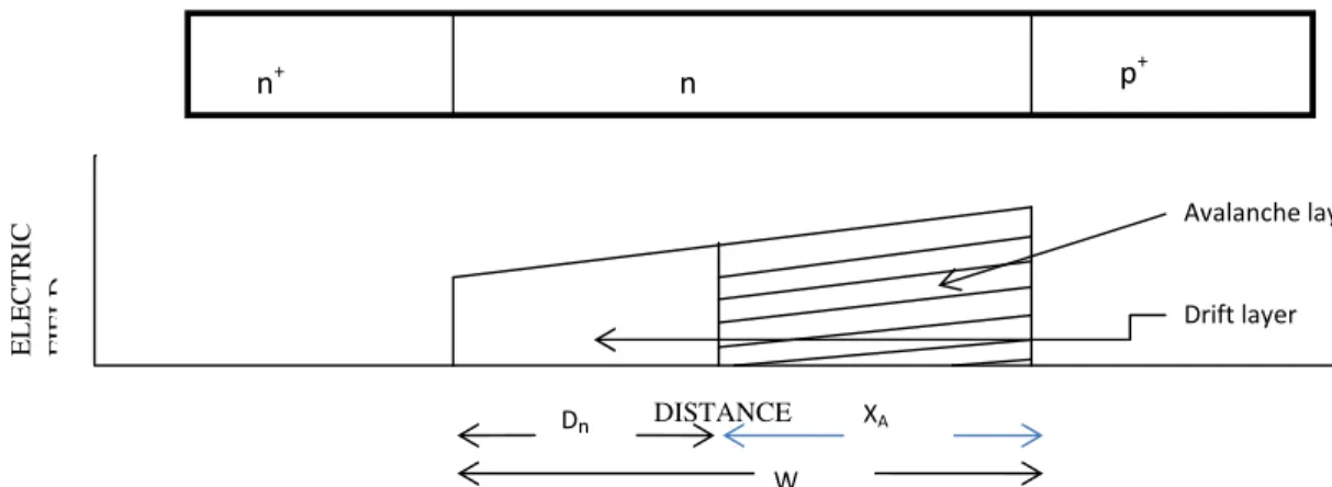
Figure 1. Schematic diode structure and electric field profile. XA=Width of the Avalanche region, Dn=Width of the Drift region, W=Total depletion layer width
Where P(x)=(Jp-Jn)/J, where Jp = hole current density , Jn = electron current density and J total current density.
Thus the dc electric field and current profiles are obtained from simultaneously solution of Poisson and carrier continuity equations, when boundary conditions (1) and (2) are satisfied. The realistic field dependence of electron and hole ionization rates, carrier mobility and the drift velocities of electron and hole are also considered in the simulation program.
The dc to mm-wave conversion efficiency [Sze et. al. 1991] is calculated from the approximate formula,
η(%) = (VD x 100)/(π x VB) (3)
Where, VD=voltage drop across the drift region. Also VD = VB – VA, where VA = voltage drop across the
avalanche region, and VB = breakdown voltage.
Avalanche breakdown occurs in the junction when the electric field is large enough such that the charge multiplication factors (Mn, Mp) become very large. The breakdown voltage is calculated by integrating
the spatial field profile over the total depletion layer width. x2
VB = − x1 ∫E(x) dx (4)
Where –x1 = n-side depletion layer width
And +x2 = p-side depletion layer width
The results of the dc analysis are then used in the small signal analysis, described briefly in the next sub-section.
n+ n p+
DISTANCE
EL
E
C
TRIC
FIE
L
D
XA
Dn
W
Avalanche layer
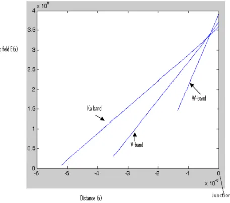
Figure 2:Electric field profiles of SDR n+ np+
IMPATT diode at Ka-band, V-band and W-band respectively.
2.2 Small signal analysis
The Gummel-Blue method [Gummel et. al. 1967] has been followed to compute the negative conductance of the diode at different frequency bands. The dc electric field and current profiles, which are obtained from the D.C analysis, are fed as input data for the small signal analysis. The real part R(x, ω) and imaginary part X(x, ω) are obtained by splitting the diode impedance Z(x, ω) using Gummel-Blue method and thus two different equations are framed [Mukherjee et. al, 2007]. Then, by using modified Runga-Kutta method the solutions of these two equations are found following a double iterative simulation scheme. The small signal parameters like negative conductance(-G), susceptance (B), impedance (Z) of the diode and the range of frequencies over which the diode exhibits negative conductance are found after satisfying the boundary conditions derived elsewhere [Kunihiro et. al. 1999, & Mukherjee et. al, 2010].
The diode negative resistance (-ZR) and reactance (-Zx) are computed through numerical integration of
the –R(x) and –X(x) profiles over the active space charge layer. Thus
x2 x2
− ZR = −x1∫ − R dx and − ZR = −x1∫ − X dx
The diode impedance Z is given by, x2
Z(ω) = − x1∫ Z( x, w) dx = −Z R + Zx (5)
The diode admittance is expressed as
Y = 1/Z = -G + jB = 1/(-ZR + jZx)
or, -G = -ZR/((ZR)2 + (Zx)2) and B = Zx/((ZR)2 + (Zx)2) (6)
-G and B are both normalized in accordance with the diode area.
The Avalanche (resonance) frequency (fa) is a frequency at which the imaginary part, susceptance (B)
of the admittance changes its nature from inductive to capacitive. The small signal quality factor (Qp) is defined
as the ratio of the imaginary part of the admittance (at the peak frequency), i.e.
-Qp= (Bp/-Gp) (7)
At a given bias current density, the peak frequency (fp) is the frequency at which the magnitude of the negative
conductance of the diode is maximum, and the quality factor is minimum. At fp, the maximum RF power (PRF)
from the device is obtained from the expression [Eisele et. al. 1997].The area of the diode is considered to be 5x10-11 m2. Under small signal condition VRF (the amplitude of the RF swing) is taken as VB/5[Majumder et. al.
3. Results and Discussions
The D.C simulation program has been used here to obtain the electric field profile [E(x)] and normalized current density profile [P(x)] of the SDR IMPATT (GaN) diode which is optimized at different mm-wave window frequency bands. The optimized design parameters of the designed diodes are summarized in table: 2
Table2: Design parameters of GaN based SDR IMPATT diodes
Diode Type Design band Epilayer doping concentration (n region) (1023 m-3)
Width of the epilayer(n region)(µm)
Current density(A/m2)
Flat doping profile
Ka (27-40 GHz)
0.35 5.2 1x10⁸
V (40-60 GHz)
0.5 3.48 1x10⁸
W (75-110 GHz)
0.9 1.25 1x10⁸
Table3: D.C and small signal analysis result
The computed electric field profiles for the designed diode are shown in fig.2.It can be seen that the value of the peak electric field Em increases with increasing the operating frequency as the width of the depletion layer
decreases at high operating frequency. It can also be seen that the ratio of drift voltage (VD) to the breakdown
voltage (VB) is highest for Ka-band diodes and then decreases for V-band and w-band diodes. More value of this
ratio will be the more localized Avalanche zone which in turns provides high efficiency. From table3.it can be seen that conversion efficiency is higher (17.9%) for Ka band diodes than that of V band (17.7%) and w band (13.9%) respectively.
The high frequency simulation program has been used to obtain the admittance characteristics (Figure 3a, 3b and 3c) and negative resistivity profiles (4a, 4b and 4c) of the designed diodes. The integrated mm-wave properties such as diode negative conductance, susceptance, RF power and quality factor can be obtained from the admittance characteristic of the SDR diodes. Figure 3a, 3b and 3c show the variation of the diode negative conductance (-G) and susceptance (B) with frequencies for various considered frequency bands. The peak operating frequencies for Ka, V and W bands are found as 38 GHz, 55GHz and 87 GHz respectively. Though the negative conductance(-Gp) value is highest for the W band diode in comparison to the other two band
diodes, the RF power contributed is of highest value for the Ka band diode (Table 3).The reason is explained as the RF power contributed by the IMPATT diode depends not only on the negative conductance (-Gp) but also on
the RF voltage (VRF) swing which in turn depends on breakdown voltage (approximately, VRF =VB/5) of the
diode which is obtained highest for Ka band diode. Results of table 3 also shows that Ka band diode perform Design
Band
Em
(108vm-1)
VD (v) VB
(v)
η (%) -Gp
(x106Sm2)
Bp
(x106S-2)
fp
(GHz) Pout
(w) -Qp
Ka 3.59 532 945 17.9 1.75 2.13 38 1.56 1.21
V 3.7 387 693 17.7 2.27 6.69 55 1.09 2.94
better than other two band diodes in terms of quality factor (Qp). To study the microscopic properties of the
diodes, the authors have computed the spatial distribution of negative resistivity [R(x)] in the depletion layer of the device, which would give an insight into the depletion region that contributes RF power. The obtained R(x) profiles at respective optimum frequencies (fp) are shown in figure 4a, 4b and 4c respectively. The computed
R(x) profiles in each case have one negative resistivity peak (R max) in the middle of the drift layers. Again from
the resistivity plot it can be seen that the resistivity peak shifts away from the junction as operating frequency increases. Which shows very good resembles with the earlier published work [Mukherjee et. al. 2005]. Moreover it is quite obvious that the contribution of negative resistivity is more from the drift region than that of the Avalanche region. This in turn indicates that drift zone contributes more mm-wave power than the avalanche zone. The results which are obtained in the present analysis shows very much similarity with earlier work done GaN (Wz) at D band[Panda et. al. 2001].The present small signal analysis thus gives useful and interesting results regarding the role of GaN (Wz) in the generation of mm-wave frequencies.
Figure 4(a)
Figure 4(b): Figure 4(c):
Figure 4: Negative resistivity [R(x)] profiles of flat doped GaN (Wz) based IMPATT diode observed in different frequency bands. (a) Plot of negative resistivity profile in Ka-band, (b) Plot of negative resistivity profile in V-band and (c) Plot of negative resistivity profile in W-band
4. Conclusions:
The simulation result provides a clear insight into the contributions of depletion layer in the generation of mm-wave power at different mm wave frequency bands for GaN based IMPATT. The analysis of this paper may be considered to be extremely helpful for the practical realization of GaN (Wz) based SDR IMPATT diodes at Ka-band and D-band for many civilian and military applications.
References:
[1] Trew R J, (2005): “High frequency solid state electronic devices”, Journal of IEEE Trans. Electron Devices vol.52, p.638.
[2] Okumura H, (2006): “Present status and future prospect of wide gap semiconductor high-power devices”, Japan. Journal of .Appl. Phys., vol.45, p.7565
[3] Inoki C K, Kaun T S, Lee C D,, Sagar A, Feenstra R M, Koleske D D,, Dfaz D Z,, Bohn P W, and Adesida I, (2003) ”Growth of GaN on porous SiC and GaN substrates”, J.Electron. Materials, vol. 32, p.855.
[4] Panda A K, Pavlidis D and Alekseev E,( 2001): “DC and high frequency characteristics of GaN based IMPATTs”, Journal of IEEE Trans. on Eletron Devices, vol.48, p.820.
[5] Eisele H and Haddad G I, (1997): Active microwave devices, Microwave Semiconductor Device Physics, New York, p.343. [6] Electronic Archive. New semiconductor materials: characteristics and properties http://www.ioffe.ru/SVA/NSM/Semicond/GaN
[7] Mukherjee M, Majumder N, Roy S K and Goswami, P.K, (2007): “GaN IMPATT Diode : a photo sensitive high power terahertz source”, Journal of Semiconductor. Science & Technology. vol.22, pp.1258-1267.
[8] Kunihiro K, Kasahara K, Takahashi Y and Ohno Y, (1999): “Experimental evaluation of impact ionization coefficients in GaN”, Journal of IEEE Electron Device Lett. Vol.20, p.608.
[9] Sze, S. M,(1991): Physics of Semiconductor Devices, second ed., Wiley Eastern Limited.
[10] Gummel H.K and Blue J.L, (1967): “Small Signal Theory of Avalanche Noise in IMPATT diodes”, Journal of IEEE Trans. on Eletron Devices, vol.14, p.569.
[11] Mukherjee M, and Roy, S. K. (2010): “Wide band gap III-IV nitride based avalanche transit time diode in terahertz regime: studies on the effects on punch through on high frequency characteristics and series resistance of the device”, Journal of Applied Physics, vol.10, pp.646-651.
[12] Mazumder, N and Roy, S. K. (1997): “Studies on pulsed mm-wave low-high-low Si IMPATT diodes at high current density and dependence on structural parameters”, Journal of Semiconductor Science & Technology, vol.12, p. 623.
[13] Mazumder N, Banerjee, J.P. and Roy S K (1989): “Variation of high frequency negative resistance of silicon n+pp+ and GaAs p+nn+ IMPATT diodes with enhancement of reverse saturation current ”, Journal of Phys. Status Solidi A, vol.116, p.415.
[14] Mukherjee M, Mazumder N and Roy S.K.,(2008): “Photo-sensitivity analysis of GaN and SiC terahertz IMPATT oscillator : comparison on theoretical reliability and study on experimental feasibility” Journal of IEEE Trans. on Device Mater Reliab., vol.8, pp. 608- 620.