Licenciado em Ciências de Engenharia Física
Optical Characterization of GaN
Dissertação para obtenção do Grau de Mestre em
Engenharia Física
Orientadores: Ana Gomes Silva, Prof. Dr., Faculdade de Ciências e Tecnologia da Universidade Nova de Lisboa
Kjeld Pedersen, Prof. Dr., Department of Physics and Nanotechnology of Aalborg University
Júri
Presidente: Prof. Dr. Isabel Catarino Arguente: Prof. Dr. Reinhard Schwarz
Copyright © José António Rodrigues Romero, Faculdade de Ciências e Tecnologia, Uni-versidade NOVA de Lisboa.
A Faculdade de Ciências e Tecnologia e a Universidade NOVA de Lisboa têm o direito, perpétuo e sem limites geográficos, de arquivar e publicar esta dissertação através de exemplares impressos reproduzidos em papel ou de forma digital, ou por qualquer outro meio conhecido ou que venha a ser inventado, e de a divulgar através de repositórios científicos e de admitir a sua cópia e distribuição com objetivos educacionais ou de inves-tigação, não comerciais, desde que seja dado crédito ao autor e editor.
Este documento foi gerado utilizando o processador (pdf)LATEX, com base no template “unlthesis” [1] desenvolvido no Dep. Informática da FCT-NOVA [2].
I would like to express my gratitude prof. Ana Cristina and prof. Kjeld Pedersen whom were very patient and persevering in helping me throughout this dissertation, both the department of Physics and Nanotechnology from Aalborg University for providing me with the required equipment, and the Physics department of Faculdade de Ciências e Tecnologia da Universidade Nova de Lisboa (FCT-UNL) for the required preparation for this work.
I would like to thank my lab colleagues Rasmus Mørch and Thore Stig for helping me with the lab equipment, and my way around the laboratory.
Gallium nitride is a direct bandgap semiconductor commonly used in LED’s and lasers. Its wide bandgap, high thermal conductivity and ability to operate at high frequencies and power make it an attractive material in the semiconductor industry.
In this thesis two different samples of gallium nitride were characterized through
four different linear and non-linear optical characterization techniques: a) optical
second-harmonic generation, b) photoluminescence c) Raman spectroscopy and d) ellipsometry. Concepts in optics for anisotropic media and non-linear crystals required for the char-acterization techniques are discussed, and three of the most commonly used epitaxial growth techniques used for GaN growth for either thin films or bulk are described.
Moreover, to complement, and validate and to get a better understanding of the experi-mental results obtained computational simulations for ellipsometry and second harmonic generation were also implemented in the Python programming language.
Raman and photoluminesence spectra were compared with other published work, allowing us to compare the crystalinity and purity of the samples. Both mathematical models for ellipsometry and second harmonic generation were fitted to the experimental results, allowing us to conclude that it is possible to determine the thickness of a thick crystal through second harmonic generation, where ellipsometry no longer is a reliable method.
Keywords: Gallium Nitride, MBE, HVPE, MOCVD, SHG, Ellipsometry,
O nitreto de gálio é um semicondutor com um hiato de energia direto geralmente utilizado em lasers e LEDs. A seu grande hiato de energia, alta condutividade térmica e elétrica, e capacidade de operar em frequências e potências elevadas o tornaram num material apelativo na indústria de semicondutores.
Nesta tese duas amostras diferentes de nitreto de gálio foram caracterizadas por qua-tro técnicas óticas lineares e não-lineares diferentes: a) Geração ótica de segunda har-mónica, b) fotoluminescência, c) Espectroscopia de Raman, e c) Elipsometría. Os conceitos de ótica em meios anisotrópicos e não-lineares necessários para as técnicas empregues são descritos, ao igual que três técnicas de crescimento epitaxial habitualmente usadas para crescer filmes e/ou cristais de nitreto de gálio.
Adicionalmente, como complemento a este trabalho foram desenvolvidos scripts na linguagem de programação Python, para simular resultados teóricos de forma a com-preender melhor os resultados experimentais obtidos neste trabalho.
Enquanto que os espectros de Raman e fotoluminescência foram comparados com outras publicações de forma a comparar a cristalinidade e pureza das amostras. Por outro lado os modelos computacionais foram adaptados aos resultados experimentais dos espectros de elipsometria e segunda harmónica, de forma a determinar a espessura de uma amostra fina e um cristal de nitreto de gálio respetivamente, demonstrando que é possível determinar a espessura de um cristal grosso através de geração de segunda harmónica onde o mesmo não seria possível através de elipsometria.
Palavras-chave: Nitreto de gálio, MBE, HVPE, MOCVD, SHG, Elipsometria,
List of Figures xiii
List of Tables xv
Acronyms xvii
1 Introduction 1
2 Electromagnetic Radiation and Optics 3
2.1 Electromagnetic Field . . . 3
2.2 Polarization of Light. . . 7
2.3 Anisotropic Medium . . . 9
2.4 Non-Linear Optics. . . 17
3 GaN Properties 25 3.1 Optical Properties . . . 26
3.2 Non-linear Properties . . . 27
3.3 Thermal and Mechanical Properties . . . 28
4 Epitaxial Growth of GaN 29 4.1 Substrate . . . 29
4.1.1 SiC . . . 30
4.1.2 Sapphire . . . 31
4.1.3 Si . . . 31
4.2 Molecular Beam Epitaxy . . . 31
4.3 Metalorganic Chemical Vapour Deposition . . . 36
4.4 Hydride Vapour Phase Epitaxy. . . 38
5 Characterization Techniques 39 5.1 Photoluminescence Spectroscopy . . . 39
5.2 Ellipsometry . . . 41
5.3 Raman Spectroscopy . . . 44
6 Experimental Procedure and Equipment 59
6.1 Photoluminescence Spectroscopy . . . 59
6.2 Ellipsometry . . . 60
6.3 Raman Spectroscopy . . . 61
6.4 Second Harmonic Generation . . . 62
7 Experimental Results and Discussion 65 7.1 Photoluminescence Spectroscopy . . . 65
7.2 Ellipsometry . . . 67
7.3 Raman Spectroscopy . . . 68
7.4 Second Harmonic Generation . . . 69
8 Conclusion 73
Bibliography 75
A Ellipsometry simulation script 79
2.1 An electromagnetic wave is composed of both a magnetic (blue wave) and
electric (red wave) fields. . . 6
2.2 Polarization ellipse for∆=π/4. . . . 8
2.3 Plane waves in an anisotropic medium travel with the direction of the Poynting vector, however the planewaves will be parallel to thekvector. . . 11
2.4 Half shell of the normal planes for a biaxial crystal.. . . 13
2.5 Intersection of the normal shells for (a) a biaxial crystal, (b) a positive uniaxial crystal and (c) a negative uniaxial crystal. . . 14
2.6 Double refraction for a biaxial crystal, wherenx < ny < nz, with an incident beam in the zx plane. . . 16
2.7 Non-linear effects observed when a crystal with a non centrosymmetric crys-tals is exposed to a beam with frequency (a)ω, (b)ω1andω2, and (c)ω1and -ω2. . . 20
3.1 The different crystal structures a GaN crystal can display. . . 25
3.2 Simulated band structure of GaN. . . 26
3.3 Vibrational modes for wurtzite GaN. . . 26
4.1 Some of the essential components that can be found on any MBE system. . . 32
4.2 Simplified scheme of a Knudsen cell. . . 33
4.3 Deposition on a target substrate with a point source geometry. . . 34
4.4 Deposition on a target substrate with a surface source geometry. . . 35
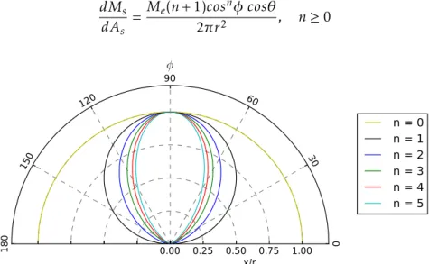
4.5 Different shapes of the vapor cloud for differentnvalues. . . 35
4.6 Schematics of two possible geometries for a MOCVD reactor. . . 36
5.1 Possible energy bandgap diagrams for semiconductors. . . 40
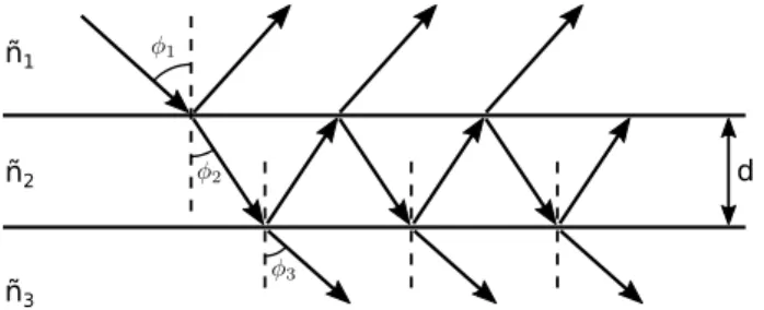
5.2 Interface between two mediums with different refractive indexes. . . . . 41
5.3 Light propagating along a two layered system with different refractive indexes. 41 5.4 Three possible vibrational modes for a CO2molecule, (a) symmetric stretch, (b) bending, and (c) anti-symmetric stretch. . . 46
5.5 Representation of the free, bound waves for a non-linear crystal. . . 52
6.2 Experimental setup used for measuring PL spectra. . . 60
6.3 Schematic of the ellipsometric system used. . . 61
6.4 Experimental setup used for Raman spectroscopy. . . 61
6.5 Experimental setups for SHG spectra.. . . 62
7.1 PL spectra obtained for both samples. . . 65
7.2 Closeup of the PL defects of the GaN on Si sample. . . 66
7.3 Experimental results for theS1ellipsometric parameter. . . 67
7.4 Experimental results for theS2ellipsometric parameter. . . 67
7.5 Raman spectra of the GaN on Si sample. . . 68
7.6 Closer look of the Raman modes found for the GaN on Si sample. . . 68
7.7 Raman modes found for the GaN single crystal sample. . . 69
7.8 SHG signal for a quartz crystal in reflection mode. . . 70
7.9 SHG signal for a quartz crystal in transmission mode. . . 70
7.10 Normalized SHG spectra for the GaN single crystal, with p-polarized light. . 71
7.11 Normalized SHG spectra for the GaN on Si sample, with s-polarized light. . 72
A.1 Refractive index and extinction coefficients used for GaN [33]. . . . . 85
A.2 Refractive index and extinction coefficients used for AlN [33].. . . 85
A.3 Refractive index and extinction coefficients used for Si [34]. . . 86
3.1 Raman active vibrational modes for wurtzite GaN [8]. . . 27
3.2 Thermal and mechanical properties of GaN [11, 12]. . . 28
4.1 Structural and thermal properties of SiC at room temperature [12].. . . 30
4.2 Structural and thermal properties of Sapphire [12]. . . 31
4.3 Structural and thermal properties of Si at room temperature [12]. . . 31
CCD Charge-coupled Device.
CVD Chemical Vapour Deposition.
HVPE Hydride Vapour Phase Epitaxy.
HWP Half Wave Plate.
IR Infrared.
LED Light Emitting Diode.
MBE Molecular Beam Epitaxy.
MOCVD Metalorganic Chemical Vapour Deposition.
MOSFET Metal Oxide Semiconductor Field-effect
Tran-sistor.
Nd:YAG Neodymium-doped Yttrium Aluminum
Gar-net.
OPO Optical Parametric Oscillator.
PBN Pyrolytic Boron Nitride.
PL Photoluminescence.
SHG Second Harmonic Generation.
UHV Ultra High Vacuum.
C
h
a
p
t
e
1
I n t r o d u c t i o n
Gallium Nitride is a group III-V compound semiconductor with a direct bandgap of 3.4 eV. Its wide bandgap has made it a popular material for optoelectronic devices such as LEDs, lasers and high power, high frequency and efficient electronic devices [1]. Only
until recently it was discovered how to successfully grow GaN films on silicon substrates, allowing GaN devices to be compatible with current Si electronic devices. Compared to Si, GaN has a higher electron mobility, a higher breakdown voltage and a higher saturation mobility allowing a better performance at higher voltages and frequencies compared to Si [2]. GaN possesses many advantages over Si, by one side the bonds in a GaN crystal are stronger, this is the reason why GaN displays a smaller electrical resistance. Electronic devices based on GaN could become much smaller and operate at much higher temperatures, which is a key factor for power applications.
Alongside GaN, some other semiconductor materials have been considered as a re-placement for Si, like SiC and GaAs. While SiC possesses a wide bandgap energy of 3.2 eV, this semiconductor can be used for high temperature and high voltages devices, however SiC price and availability make it less appealing as the next replacement of Si, making GaN the future option for widespread electronic devices and leaving SiC for higher end applications where the cost of production may not be the main concern [3]. GaAs is an-other popular semiconductor for making electronic devices such asLight Emitting Diodes (LEDs), lasers, solar cells, among many other applications, however its sole advantage is the fact that it is cheaper to mass produce and benefits from a more extensive period of research compared to GaN. Nonetheless GaN has proven to allow higher efficiencies, also
it can operate at higher temperatures and higher voltages than GaAs, and at the same time adoption of GaN will likely make mass production of GaN a more affordable solution,
likely replacing GaAs from the market.
the optimal characteristics in the produced films it’s necessary to understand the growth processes used, and how it may affect the characteristics of the film. Once produced, it’s
also necessary to characterize these films to determine whether or not they obey fit the required criteria for their intended application. The characterization of the samples is done through performing several techniques, each of them providing a set of information of our samples.
Although gallium nitride is still a material which requires a more detailed under-standing, specially when it comes to its production, some GaN devices can be currently found in the market, devices such as LEDs with wavelengths between the blue and UV spectra by adding aluminum or in the visible region by adding indium. GaN powerMetal Oxide Semiconductor Field-effect Transistors (MOSFETs)can also be found since they
display a better relationship between on-resistance and breakdown voltage compared to its silicon counterpart [4].
C
h
a
p
t
e
2
E l e c t r o m a g n e t i c R a d i a t i o n a n d O p t i c s
Most of the characterization methods applied for thin films consist on determining many of the optical properties of the films, this is due the fact that most of these characterization methods are non-destructive and contactless methods which is highly advantageous for these kind of devices that highly depend on the degree of purity and crystal quality of the layers, also the fact that the same sample can be reutilized on all these techniques is also a great advantage since the time and money required to produce these films can prove to be an inconvenient.
2.1
Electromagnetic Field
In classic electromagnetism, an electromagnetic field can be described by two fields, and those are the E andH which are the electromagnetic and magnetic field respectively.
These fields obey a set of differential equations which are called Maxwell’s equations.
These equations are:
∇ ×E+∂B
∂t = 0 (2.1.1)
∇ ×H−∂D
∂t =J (2.1.2)
∇ ·D=ρ (2.1.3)
∇ ·B= 0 (2.1.4)
The first equation is known as Faraday’s law of induction, establishing that a non-conservative electric field will always induce by a time dependent magnetic field and vice-versa. The Electric field is said to be non-conservative because otherwise it’s curl would equal to zero, which means that this same field cannot be spacially constant.
Eq.2.1.2is known as Ampère’s law, and establishes that any current or any changes in time of the electric displacement will induce a non-conservative magnetic field and vice versa, in other word any charge flow will induce a magnetic field in the area they pierce. Both Equations 2.1.3and 2.1.4are Gauss’s law for electric and magnetic fields re-spectively, the first one describes that the electric field that pierces a closed surface is proportional to the charge that is contained inside that same volume, the second one establishes the non existence of magnetic monopoles since the total magnetic flux that pierces a closed surface must always equal to zero (if there were any monopoles the divergence of the magnetic field in a volume could equal a value different that zero).
These same equations can also be expressed in their integral form opposed to the dif-ferential form applying both Gauss’s divergence theorem (Eq.2.1.5) and Stoke’s theorem (Eq.2.1.6), which allows to switch from a volume integral to a surface integral and from a surface integral to a line integral respectively.
*
V
(∇ ·F)dV = ∂V
F·dS (2.1.5)
S
(∇ ×F)·dS=
I
∂S
F·dl (2.1.6)
Where∂S and∂V represent the boundary of the closed surfaceS and closed volume V respectively. Applying both Equation2.1.5on Equations2.1.3and2.1.4, and2.1.6on Equations2.1.1and2.1.2, these same can also be written as:
I
∂S
E·dl=−
S ∂B
∂t ·dS (2.1.7)
I
∂S
H·dl= S
J+∂D ∂t
!
·dS (2.1.8)
∂V
D·dS=
*
V
ρ dV (2.1.9)
∂V
B·dS= 0 (2.1.10)
These set of differential equations dictate the basis for classical electrodynamics and
optics as well as electrical circuits. However before applying these equations it is nec-essary to know how the material respond to an electromagnetic field, this effect on the
material is given by the electromagnetic constitutive equations for that given material.
D=εE=ε0E+P (2.1.11)
Where Eq.2.1.11 is the electric displacement field and establishes how a medium reacts to an electric field, whereεis the permitivity of the medium,ε0is the permitivity of vacuum and P is the electric polarization, and Eq.2.1.12 is the magnetic field and
establishes the interaction with a magnetic field where µis the permeability, µ0 is the permeability of vacuum andMis the magnetic polarization.
Throughout this subsection only linear mediums are going to be discussed, which means that both the magnetic and electric polarization are going to be proportional to the electric and magnetic field respectively. The same can be written as:
P=ε0χeE =⇒ D=ε0(1 +χe)E (2.1.13)
M=µ0χvH =⇒ B=µ0(1 +χv)H (2.1.14)
Whereχe andχv are the electric and magnetic susceptibility respectively. As men-tioned these equations assume a linear response of the medium, which will be valid for this subsection, and later on subsection2.4this assumption will no longer be valid, also only the electric polarization will be taken into account since the electric field in electromagnetic radiation is usually far stronger than the magnetic field, therefore the polarization intensity can be described as only the electric polarization. A material is said to be homogeneous if bothχeandχv are independent of the position, also the medium is said to be isotropic if both susceptibilities can be expressed as scalar quantities, otherwise both vectorsPandD, and vectorsMandBwould not be parallel to each other and the medium is said to be anisotropic.
Most of electromagnetic waves can be expressed as sinusoidal waves, and can be either expressed by a pure real sinusoidal function or as a complex exponential function, where the real part would correspond to the same wave as the pure real counterpart. Let’s take an electric field given by the following expression:
E=E0ei(k·r−ωt) (2.1.15)
The electromagnetic wave is said to be monochromatic is we assumeωto be a constant, therefore having a constant wavelengthλ. If we apply Gauss’s law, and assume that the medium is both homogeneous and there are no free charges, thusρ= 0, we also obtain:
∇ ·D=ρ =⇒ ∇ ·E=ρ
ε =⇒ ∇ ·E= 0 (2.1.16)
=⇒ ∇ ·(E0ei(kxx+kyy+kzz−ωt)) = 0 (2.1.17)
=⇒ E0·k= 0 (2.1.18)
can also be expressed through complex equations since they also behave as sinusoidal waves just as electric fields, and through Faraday’s law it is possible to determine the magnetic field direction.
B=B0ei(k·r−ωt) (2.1.19)
∇ ×E=−∂∂tB =⇒ ik×E=−∂∂tB (2.1.20)
=⇒ B= 1
ωk×E (2.1.21)
Therefore it is possible to conclude that both the electric field and the magnetic field are perpendicular to each other and perpendicular to the direction of propagation of the wave.
E0
B0
λ
k
Figure 2.1: An electromagnetic wave is composed of both a magnetic (blue wave) and electric (red wave) fields.
Electromagnetic waves conservation of energy is also observed, this conservation of energy is expressed by Poynting’s theorem, where it is established that the rate of change on time of the energy density on a closed volume for an electromagnetic field must equal to the flux of energy leaving that volume plus the work done to the free charges (or the free charge density) on the same volume. This theorem can be expressed as follows:
−∂U∂t =∇ ·S+J·E (2.1.22)
WhereU is the energy density per unit of volume of the electromagnetic field andS
is the Poynting vector, and the same are defined as:
U=1
2(E·D+H·B) (2.1.23)
However these equations are only true for non-complex equations, otherwise these quantities are expressed as follows:
U=1
4Re[E·D∗+B·H∗] (2.1.25)
S=1
2Re[E×H∗] (2.1.26)
The Poynting vectorSrepresents the direction of the energy flux of an
electromag-netic wave, this flux will have the same direction as the propagation of the wave, and the magnitude of this vector represents the power density per unit of area, therefore integrat-ing this vector along a closed surface A this same vector pierces would give us the rate flow of energy along the same surface.
Prad= I
A
S·dA (2.1.27)
In Eqs.2.1.15and2.1.19, a wave vectorkwhich propagates along the principal axis given by the vectorrwas introduced. This wavevector k is the vector of propagation in the medium, however the speed on how this wavevector propagates will depend on the refractive index of the material, and also all glasses display dispersion phenomenons, and what this means is that the refractive index of the material will vary with the wavelength of the incident beam.
k=n(ω)ω
c (2.1.28)
This refractive index can be either a real number for a lossless medium, or a complex number, which depending on its extinction coefficientκcan be either an attenuating or
stimulated amplifying medium, ifκ possesses a negative or positive value respectively. This complex refractive index can be written as:
˜
n=n+iκ (2.1.29)
2.2
Polarization of Light
Let’s assume an electromagnetic wave with itskvector in the z direction given by the following function:
E=Re[E0ei(ωt−kz)] (2.2.1)
Given that the wave propagates on the z direction, both electric and magnetic fields can only be contained in either the x or y planes, therefore the electric field can be sepa-rated in both a x and y components.
The respectiveExandEy of the electric field are then given by:
Ex=E0xcos(ωt−kz+∆x) (2.2.2)
Ey=E0ycos(ωt−kz+∆y) (2.2.3)
These two expression can be further simplified in one single expression, relating both ∆xand∆y, through some simple algebra.
Ex E0x
!2 + Ey
E0y
!2
−2cos(E ∆) 0yE0x
ExEy= sin2∆ (2.2.4)
∆=∆y−∆x, ∆∈[−π, π] (2.2.5)
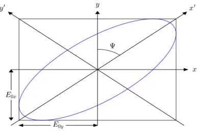
Looking at Eq.2.2.4, the curve of this equation will be a ellipse, and the orientation of the ellipse will dictate the polarization state of the wave. From this curve, there are two special cases, when the ellipse is either a straight line or a circle, in which cases the light is said to be linearly and circularly polarized.
x
y x′
y′
Ψ
E0x
E0y
If an electromagnetic wave is linearly polarized then:
∆=∆y−∆x=nπ, n= 1,2 (2.2.6)
Otherwise the electromagnetic wave is said to be circularly polarized if:
∆=∆y−∆x=nπ
2, n=−1,1 (2.2.7)
The electric field for both x and y components can also be written in a complex func-tion, so that a complex ratioρbetween bothEyandExis given by:
Ey =E0yei(ωt−kz+
∆y)
(2.2.8)
Ex=E0xei(ωt−kz+
∆x)
(2.2.9)
ρ=Ey Ex
=ei∆tanΨ=E0y E0xe
∆y−∆x
, Ψ∈[0, π/2] (2.2.10)
2.3
Anisotropic Medium
Through section2.1the media was assumed to be isotropic, and as a consequence, the electric polarization vector P was assumed to be parallel to the induced electric field.
However there are many materials that do not display this behavior such as calcite, quartz, KDP and liquid crystals [5]. Looking at Eq.2.1.13, the electric polarization in given as:
P=ε0χeE (2.3.1)
However for this equation hold true for anisotropic media, then the electric suscep-tibility must be then given by a rank 2 tensor, otherwise the electric polarization vector would always be parallel to the induced electric field, therefore the electric susceptibility can be written as:
χe=
χ11 χ12 χ13
χ21 χ22 χ23
χ31 χ32 χ33 (2.3.2)
Therefore the electric displacement vector will be given as
D=ε0(1 +χe)E=εE=
ε11 ε12 ε13
ε21 ε22 ε23
ε31 ε32 ε33 · Ex Ey Ez (2.3.3)
Di=
3 X
j=1
It is possible to demonstrate through conservation of energy as stated on Poyting’s the-orem that the dielectric tensor must be symmetric, so that there are only six independent term on the dielectric tensor matrix, therefore:
εij=εji, i, j= 1,2,3 (2.3.5)
However it is possible to choose a set of coordinates x y and z for the crystal so that non-diagonal members of the matrix are set to be zero, this set of coordinates are called the principal axis of the system, further simplifying the dielectric tensor as:
ε=
εx 0 0
0 εy 0
0 0 εz
(2.3.6)
For this matrix there are three possibilities:
εx=εy=εz (2.3.7)
εx=εy,εz (2.3.8)
εx,εy,εz (2.3.9)
The first case is the same as studied before, an isotropic medium, where this same matrix could be also written as just simply a scalar, for the second case the medium is said to be uniaxial crystal and for the third case a biaxial crystal.
Let’s assume an electric field and a magnetic field given by the following expressions:
E=E0ei(k·r−ωt) (2.3.10)
H=H0ei(k·r−ωt) (2.3.11)
Applying Maxwell’s Eqs.2.1.1and2.1.2, andassuming there are no free charges, we get:
k×E=ωµH (2.3.12)
k×H=−ωεE (2.3.13)
k S D
E
H
Figure 2.3: Plane waves in an anisotropic medium travel with the direction of the Poynt-ing vector, however the planewaves will be parallel to thekvector.
Through Eqs.2.1.12and2.1.21, Eq.2.3.12can be further simplified as:
B= 1
ωk×E, B=µH =⇒ µH= 1
ωk×E (2.3.14)
=⇒ k×(k×E) =−ω2µ εE (2.3.15)
=⇒ (k·E)k−(k·k)E=−ω2µ εE (2.3.16)
Where just likeε,µis a diagonal rank 2 tensor, which can be expressed as a constant for isotropic mediums.
ε=
εx 0 0
0 εy 0
0 0 εz
, µ=
µx 0 0
0 µy 0
0 0 µz
(2.3.17)
From Eqn.2.3.16we then get that:
ω2µxεx−ky2−kz2 kxky kxkz kykx ω2µyεy−kx2−kz2 kykz kzkx kzky ω2µzεz−kx2−ky2
· Ex Ey Ez
= 0 (2.3.18)
ω2µxεx−ky2−kz2 kxky kxkz kykx ω2µyεy−kx2−kz2 kykz kzkx kzky ω2µzεz−kx2−ky2
= 0 (2.3.19)
Expanding this determinant a quadratic expression forω2 will be found, however only two of the four roots will be real ones, which will correspond to the two independent states of polarization for the propagation of the wave. By simplifying this determinant we then get:
kx2 k2−ω2µxεx
+ ky
2
k2−ω2µyεy
+ kz
2
k2−ω2µzεz
= 1 (2.3.20)
By simplifying Eq.2.3.18, the direction of the electric field can be obtained.
Ex Ey Ez
=E0 kx k2−ω2µxεx
ky k2−ω2µyεy
kz k2−ω2µzεz
(2.3.21) where
E0=kxEx+kyEy+kzEz=k·E (2.3.22)
k2=kx2+ky2+kz2 (2.3.23)
Since the medium is said to be anisotropic, each principal axis will have its own refractive index, this is, the refractive index of the system will also be given as a rank 2 tensor, which is given by:
n=
nx 0 0
0 ny 0
0 0 nz
= r 1 ε0µ0
√ε
xµx 0 0
0 √εyµy 0
0 0 √εzµz
(2.3.24)
Thekvector for a given anisotropic medium can be written as:
Wheresis an unitary vector with the direction of propagation, and n is the effective
refractive index. With both Eqs.2.3.24and2.3.25it is possible to write Eq.2.3.20as:
sx2 n2−n2x
+ s
2
y n2−n2y
+ s2z n2−n2z
= 1
n2 (2.3.26)
and Eq.2.3.21as:
Ex Ey Ez
=n2(s·E) sx n2−nx2
sy n2−ny2
sz n2−nz2
(2.3.27)
Plotting Eq.2.3.20in thek space, two shells will appear, with a maximum of four common points, depending on the values ofnx,ny andnz.
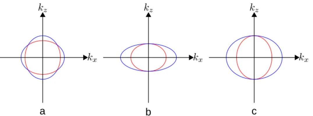
Figure 2.4: Half shell of the normal planes for a biaxial crystal.
For a biaxial crystal, intersecting the shells on the xz plane, will end up in two el-lipsoids with four common points, these four points will set up the two optical axis of the crystal, so for a biaxial crystal two symmetry axis on thekspace will be found (thus
a b c
Figure 2.5: Intersection of the normal shells for (a) a biaxial crystal, (b) a positive uniaxial crystal and (c) a negative uniaxial crystal.
From Eq.2.1.23we know that the energy density is given as:
U=1
2(E·D+H·B) (2.3.28)
So it is possible to separate this energy density in both a magnetic and electric part.
U=1
2(UE+UB) (2.3.29)
So if we look at the electric component of the energy density we get that:
2UE =
ε−1D
·D ⇐⇒ 2UE=D
2
x εx +
Dy2 εy +
Dz2
εz (2.3.30)
⇐⇒ 1 = 21U e
Dx2 εx
+D 2
y εy
+Dz2 εz (2.3.31)
⇐⇒ 1 = x 2
εx +y2
εy +z2
εz
(2.3.32)
Where
r=√2D UE =
x y z (2.3.33)
However if we assume our crystal to be non-magnetic, then this would translate as:
1
Then our refractive index tensor of our crystal can be further simplified as:
n=√1 ε0 √ε
x 0 0
0 √εy 0
0 0 √εz
(2.3.35)
Then our electric displacement vector would yield:
D=εE=ε0
n2x 0 0
0 n2y 0
0 0 n2z
·E (2.3.36)
Then Eq.2.3.32can be further simplified as:
1 = x2 ε0n2x
+ y2 ε0n2y
+ z2 ε0n2z
(2.3.37)
However since ε0 is a constant and to allow for a more compact notation, we then redefineras:
r=√ D 2ε0UE
= x y z (2.3.38)
Then Eq.2.3.32would instead be given as:
x2 n2x
+y2 n2y
+ z2 n2z
= 1 (2.3.39)
This equation is known as the index ellipsoid or the optical indicatrix, and it serves as a graphical representation of the relative magnitude of the refractive indices for each direction of the crystal.
So for an uniaxial crystal, wherenxandnyequal each other, Eq.2.3.39can be rewritten as:
x2 n2o
+y2 n2o
+ z2 n2e
= 1 (2.3.40)
where
no=nx=ny (2.3.41)
Since the normal shell for anisotropic media consists in two shells, which correspond to the two independent solutions for the polarization of the refracted waves for a given direction, then for an incident wave two refracted waves are going to be observed if the incident polarization consists of a linear combination of these two independent states.
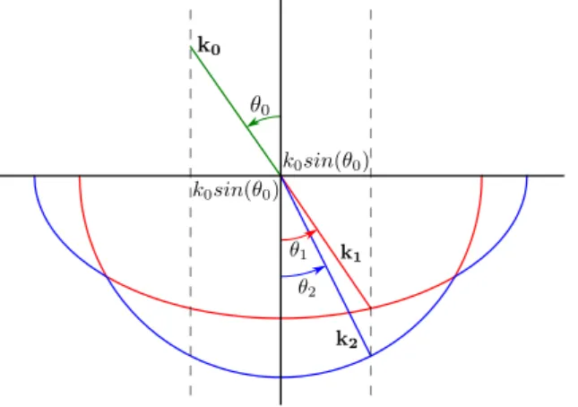
Let us then consider a given anisotropic crystal with an incident wave withk0as its propagation vector, andθ0as the angle betweenk0and the normal of the crystal surface, then the kinematic conditions for the refracted waves are given as:
k0sin(θ0) =k1sin(θ1) =k2sin(θ2) (2.3.43)
Wherek1andk2are the propagation vectors for both refracted waves andθ1andθ2 are their respective angles between the normal of the crystal surface.
Figure 2.6: Double refraction for a biaxial crystal, wherenx < ny < nz, with an incident beam in the zx plane.
For an isotropic crystal we know that our normal shell consists of two overlapping spheres, so the values ofk1andk2not only are going to equal each other, as they will not depend on the direction of propagation, however this will not be true for anisotropic media, thus resulting in a double refraction of light.
For an uniaxial crystal, one of the shells of the normal surface is always a sphere, so one of the solutions for the refracted waves will not depend on its direction of propagation, just like on an isotropic crystal, so for a given incident wave we can split this wave in the sum of two other waves, where one of these waves will have a parallel polarization with regards the optical axis of the crystal and the other one a perpendicular polarization, when refracted, the perpendicular component will follow Snell’s law, and the refractive index for this refraction is called the ordinary refractive index (no), while the other refracted (or extraordinary ray) will not follow Snell’s law. So for the ordinary ray we get:
Whereniis the refractive index of the medium from the wave came before our crystal (usually 1 since its the air’s refractive index).
2.4
Non-Linear Optics
Throughout this chapter all media were assumed to respond linearly to a electromagnetic field, however this assumption may not be valid for all crystals, so when exposed to an electromagnetic field, the induced polarization on the medium can be expressed in Taylor series, where the higher order terms will be responsible for any non-linear behavior. This non-linear behavior predominantly arises when the applied electric field is strong when compared to the atomic bonds of the crystal.
Let us then consider the polarization vector, where theith component of this vector is given as:
Pi= 3 X
j=1
ε0χ(1)ij Ej+
3 X
j=1 3 X
k=1
ε0χ(2)ijkEjEk+
3 X
j=1 3 X
k=1 3 X
l=1
ε0χ(3)ijklEjEkEl+... (2.4.1)
In order to allow a more compact notation this same polarization component can be written as:
Pi=ε0χij(1)Ej+ε0χ(2)ijkEjEk+ε0χ(3)ijklEjEkEl+... (2.4.2)
So looking at this equation, it can be seen that there are several non-linear coefficients,
and while the third order coefficientχ(3)
ijkl is always present for any material (although since its a higher order term its values can be really small for some materials, so that these materials can be studied as if they behaved linearly), while the second order term depending on the symmetry of the crystal may be zero, for instance centrosymmetric crystals will always have a zero second order non-linear coefficient.
Let us assume a given crystal with a centrosymmetric structure, if this same crystal is exposed by an electromagnetic wave, then inversion of symmetry must be observed (otherwise it wouldn’t be a centrosymmetric crystal). Then P and E can be replaced
in Eq.2.4.2 with −P and −E respectively, and the ith component must also verify the following equation:
−Pi=ε0χij(1)(−Ej) +ε0χ(2)ijk(−Ej)(−Ek) +ε0χ(3)ijkl(−Ej)(−Ek)(−El) +... (2.4.3)
=−ε0χij(1)Ej+ε0χ(2)ijkEjEk−ε0χ(3)ijklEjEkEl+... (2.4.4)
Comparing Eq.2.4.2and Eq.2.4.4we then get:
SinceEis an arbitrary vector andε0a constant, this means that the only way for the same equation to be held true is if the second order coefficient is admitted to be zero,
in fact if we were to consider a fourth order term the same would also equal zero for centrosymmetric crystals, so all even parity coefficients would equal zero for this kind
of crystals. However this theory only applies if we only consider dipolar electrical inter-actions, discarding any dipolar magnetic, or any quadrupolar or higher order electrical interaction (which is the case in this analysis).
The second order non-linear behaviour of a crystal will be responsible for effects such
asSecond Harmonic Generation (SHG), frequency summation and differentiation, optical
rectification, parametric amplification and oscillation [5]. Third order non-linear effects
include Raman and Brillouin scattering, third harmonic generation, self focusing, and optical phase conjugation [5]. In this chapter we will only focus second order non-linear interactions, so third order interaction or higher order interactions will not be considered. Let us now assume that the polarization of a given crystal is given by only the first two terms of our Taylor expansion.
Pi=ε0χ(1)ij Ej+ε0χ(2)ijkEjEk (2.4.6)
One important side note that must be taken care of, is the use of complex notation for describing the electric field, since the product of two complex numbers alter the real part. So for instance thejth component of the electric field could be written as:
Ej(t) =Re(Ej0ei(k·r−ωt)) =12(Ej0ei(k·r−ωt)+c.c.) (2.4.7)
Wherec.c.stands for the complex conjugate of the electric field equation. Lets con-sider that our electric field can be expressed just as a scalar quantity, then we can define our electric field as:
E=E0cos(k·r−ωt) (2.4.8)
Then the polarization would be given as:
P=ε0χ(1)E0cos(k·r−ωt) +ε0χ(2)E02cos2(k·r−ωt) (2.4.9)
=ε0χ(1)E0cos(k·r−ωt) +12ε0χ(2)E02(1 +cos(2(k·r−ωt))) (2.4.10)
a non-zero value, thus the crystal will have a preferential direction for its polarization vector. The materials that exhibit this behaviour are said to have a quasi-DC polarization, and this phenomena is commonly referred as optical rectification. The second aspect is the fact that a harmonic electric dipole moment component with frequency 2ωappears, so the oscillating dipoles not only are going to have a preferential direction because of the time-independent term, their oscillations will be given as a superposition of two harmonic components with frequenciesωand 2ω.
Since an oscillating electric dipole emits electromagnetic radiation, this crystal will emit radiation with both frequenciesωand 2ω, so in fact a non-linear crystal can be used to generate an output beam of light with a frequency higher than its input beam, in this case twice the frequency to be precise, thus this phenomena is called second harmonic generation.
Let us then consider an electromagnetic wave which consists on the superposition of two waves of frequenciesω1andω2respectively. Then our electric field can be written as:
E=E1cos(k1·r−ω1t) +E2cos(k2·r−ω2t) (2.4.11)
Then our second order polarization term is given as:
P(2)=ε0χ(2)(E1cos(k1·r−ω1t) +E2cos(k2·r−ω2t))2 (2.4.12)
= ε0χ
(2)(E2
1cos2(k1·r−ω1t) +E1E2cos(k1·r−ω1t)cos(k1·r−ω2t) +E22cos(k2·r−ω2t))
(2.4.13)
Expanding further this equation, similarly like the previous one, a time independent term will arise and two harmonic terms with frequencies 2ω1and 2ω2respectively will also appear, however a harmonic term with frequencyω1+ω2will also appear which in this case its known as a phenomena known as frequency summation. Similarly if we take an electric field defined as:
E=E1cos(k1·r−ω1t)−E2cos(k2·r−ω2t) (2.4.14)
Then a harmonic term with frequencyω1−ω2will appear, and in this case the phe-nomena is know as frequency differentiation. So in order for frequency summation or
differentiation to be observed it is necessary to have at least two frequencies in our input
beam, otherwise only second harmonic generation would be observed. However in order to have a high efficiency conversion for these non-linear effects, a set of phase matching
b
c
a
Figure 2.7: Non-linear effects observed when a crystal with a non centrosymmetric
crys-tals is exposed to a beam with frequency (a)ω, (b)ω1andω2, and (c)ω1and -ω2.
Let us take for another example an other electromagnetic wave, with its electric field defined as:
E=E1cos(k1·r−ωt) +E2cos(k2·r−2ωt) (2.4.15)
By replacing this electric field in the second order non-linear polarization equation we get five different terms. The first term is a time-independent term responsible for the
optical rectification, while the other four terms are time dependent harmonic terms with frequencies ω, 2ω, 3ωand 4ωrespectively. As previously stated the efficiency of these
frequencies conversion is dependent on a set of phase matching conditions, however each frequency has its own phase matching conditions, that may or may not be the same for each frequency, thus while some terms might experience a high efficiency conversion
other terms might not, thus the terms with negligible efficiency are often excluded.
We can rewrite the polarization as the sum of a linear and non-linear terms:
P=PL+PNL=ε0χ(1)E+PNL (2.4.16)
Where theith component of the non-linear polarization vector is given as:
(PN L)i=ε0χ(2)ijkEjEk (2.4.17)
By replacing this non-linear polarization in Maxwell’s equations, and if we assume there are no free charges or free currents in our material, we then get that:
∇ ·E= 0 (2.4.18)
∇ ·B= 0 (2.4.19)
∇ ×E=−∂∂tB (2.4.20)
∇ ×H=∂D ∂t =
∂
To further simplify this relation, let us look at the following expression:
∇ ×(∇ ×E) =∇(∇ ·E)− ∇2E (2.4.22)
=−∇2E (2.4.23)
By replacing with our previous Maxwell’s equations we get that:
∇ × −
∂B
∂t
=−
∆E (2.4.24)
∇2E=µ0
∂
∂t(∇ ×H) (2.4.25)
=µ0ε0
1 +χ(1)
∂2E
∂t2+µ0 ∂2PNL
∂t2 (2.4.26)
This condition must be met for both the waves withωand 2ωfrequencies.
∇2E(ω)=µ0ε0 1 +χ((1)ω) !
∂2E(ω)
∂t2 +µ0 ∂2P(NLω)
∂t2 (2.4.27)
∇2E(2ω)=µ0ε0 1 +χ(2(1)ω) !
∂2E(2ω)
∂t2 +µ0
∂2P(NL2ω)
∂t2 (2.4.28)
This two equations dictate how the electromagnetic wave propagates in a non-linear media, however while in a linear media these two waves would propagate without in-teracting with each other, the non-linear polarization terms binds these two equations together, and these same non-linear polarization terms dictate how the two waves inter-act. A non-linear polarization term might lead to the generation of a different frequency,
which would also need to satisfy this same conditions, thus these two set of equations need to be solved simultaneously.
Let us assume that both our waves atω and 2ωfrequencies travel along the z axis exclusively, then the electric field for these equations can be written as follows:
E(ω)=1 2
E1ei(k1z−ωt)+c.c.
(2.4.29)
E(2ω)=1 2
E2ei(k2z−2ωt)+c.c.
(2.4.30)
So the total electric field on our crystal would be given as:
Then the non-linear polarization term for our crystal would be given as:
PN L=14ε0χ(2)
E1ei(k1z−ωt)+E2ei(k2z−2ωt)+c.c. 2
(2.4.32)
By further expanding this non-linear polarization term, terms with frequenciesωand 2ωcan be found, and they are given as follows:
PN L(ω)= 1 2
ε0χ(2)(ω)E2E1∗ei((k2−k1)z−ωt)+c.c.
(2.4.33)
PN L(2ω)= 1 4
ε0χ(2)(2ω)E21e2i(k1z−ωt)+c.c.
(2.4.34)
It is important to take notice on bothE1andE2when dealing with these non-linear media, since both terms will also be functions ofz, otherwise our non-linear polarization term would then equal to zero, and said crystal would be considered a linear medium. Lets us assume that for the electromagnetic waveE(ω),E1is in fact independent of thez axis, then:
∂2E(ω) ∂z2 =−k
2
1E(ω)=−
k12 −ω2
∂2E(ω) ∂t2 =
ω2 c2ω2εr(ω)
∂2E(ω)
∂t2 (2.4.35)
=µ0ε0
1 +χ(1)(ω)∂2E(ω)
∂t2 (2.4.36)
The only way forE(ω) to satisfy Eq.2.4.27would only be if its non-linear term PN L(ω) equals to zero, thus if our crystal is said to be a non-linear medium, thenE1 must be a function ofz, otherwise the wave equation conditions for our crystal would not be met. So in order to fully study any non-linear process in our medium it is then necessary to obtain an expression for both ∂2E(ω)
∂z2 and ∂2E(2ω)
∂z2 , however in some cases where the efficiency of the second harmonic signal is very small compared to theωfrequency signal, then ∂2E(ω) ∂z2 can be considered as constant to further simplify calculations.
Expanding these two partial derivatives we then get:
∂2E(ω) ∂z2 =
∂2E1
∂z2 + 2ik1
E1
∂E1
∂z +k
2 1 !
E(ω)= ∂2E1 ∂z2 + 2ik1
∂E1
∂z
!
E(ω)+n2ω c2
∂2E(ω)
∂t2 (2.4.37)
∂2E(2ω) ∂z2 =
∂2E2
∂z2 + 2ik2
E2
∂E2
∂z +k
2 2 !
E(2ω)= ∂
2E 2
∂z2 + 2ik2 ∂E2
∂z
!
E(2ω)+n
2 2ω c2
∂2E(2ω)
∂t2 (2.4.38)
By comparing this expressions with Eqs.2.4.27and2.4.28, we get:
∂2E1
∂z2 + 2ik1 ∂E1
∂z
!
E(ω)=µ0∂ 2P(ω)
N L
∂t2 (2.4.39)
∂2E2
∂z2 + 2ik2 ∂E2
∂z
!
E(2ω)=µ0∂ 2P(2ω)
N L
If we assume that bothE1andE2have a small variation onzso that:
∂2E1
∂z2 ≪k1 ∂E1
∂z (2.4.41)
∂2E2
∂z2 ≪k2 ∂E2
∂z (2.4.42)
Then the following approximations can be considered:
2ik1∂E1
∂z E
(ω)=µ 0∂
2P(ω)
N L
∂t2 (2.4.43)
2ik2∂E2
∂z E
(2ω)=µ 0∂
2P(2ω)
N L
∂t2 (2.4.44)
By simplifying these equations we then get:
∂E1
∂z =i ω 2cnω
χ((2)ω)E2E1∗ei∆kz+c.c. (2.4.45)
∂E2
∂z =i ω 2cn2ωχ
(2) (2ω)E12e−i
∆kz
+c.c. (2.4.46)
where
∆k=k2−2k1 (2.4.47)
Now if we assume that our input source only emits radiation with frequencyω, this means that our non-linear polarization term for 2ωmust be our source of radiation at 2ω frequency.
By looking at this non-linear polarization term, it is possible to see that in fact it is also a traveling wave, thus it must also posses its own phase velocity, which is given as:
νp
PN L(2ω)
= 2ω
2k1 (2.4.48)
Then this phase velocity should be equal to the phase velocity ofE(2ω)
νp
E(2ω)=2ω k2 =⇒
2ω k2 =
2ω
2k1 (2.4.49)
=⇒ ∆k= 0 (2.4.50)
This condition is called the phase matching condition, and it ensures that the interfer-ence betweenE(2ω)andPN L2ωis always constructive, so when∆k= 0 then the efficiency of
C
h
a
p
t
e
3
Ga N P r o p e rt i e s
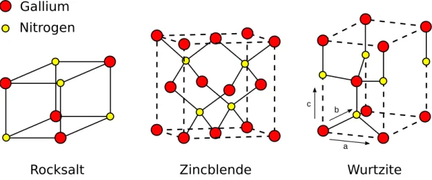
Three different crystal structures can be achieved with GaN, and these are rocksalt,
zincblende and wurtzite structures, however only the later one is stable for GaN, the other two structures are meta-stable structures which means that these structures will not be found in GaN films grown in stable conditions [6]. This wurtzite structure is asymmetrical on the c direction, which will lead to a polarization on the crystal since both the gallium and nitrogen atoms tend to form ionic bonds, this polarization of the material is called spontaneous polarization. This polarization can be highly increased by moving the atoms from their equilibrium position, this piezoelectric polarization can be achieved through a misfit of ether in the lattice or thermal expansion coefficient mismatch
in hetero-structures or by adding impurities on the crystal [6].
Rocksalt
Zincblende
Gallium
Nitrogen
Wurtzite
ab c
3.1
Optical Properties
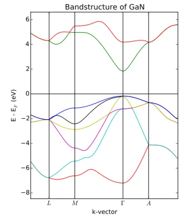
GaN possess a wide bandgap of 3.4 eV, and unlike silicon, it is a direct bandgap semi-conductor, which is a desirable trait for the semiconductor industry.
L M Γ A
k-vector 8
6 4 2 0 2 4 6
E
-
EF
(
eV
)
Bandstructure of GaN
Figure 3.2: Simulated band structure of GaN.
For wurtzite GaN there are four possible optical vibrational modes, these areA1,E1, 2E2 and 2B2. While bothA1 andE1 are polar modes (thus they are both Raman and
Infrared (IR)active modes),E1modes are non-polar modes thus only Raman active,B1 modes however are silent modes and aren’t either Raman orIRactive [7,8].
Both polar modes can be either transversely or longitudinally polarized (TO and LO respectively), and for each polarization state a different energy is associated. However
depending on the scattering geometry only some of these vibrational modes are visible due to selection rules, which are described on the following table:
Mode Configurations Wavenumber (cm−1)
A1(T O) x(y, y)x,x(z, z)x,y(x, x)y,y(z, z)y 531.8
A1(LO) z(x, x)z,z(y, y)z 734.0
E1(T O) x(z, y)x,x(y, z)y 558.8
E1(LO) x(y, z)y 741.0
E2H z(x, x)z,z(x, y)z,x(y, y)x 567.6
E2L z(x, x)z,z(x, y)z,x(y, y)x 144.0
Table 3.1: Raman active vibrational modes for wurtzite GaN [8].
Thus for incident light on the (0001) plane of the wurtzite crystal plane, only the vibrational modesA1(LO) and both E2 modes should be observed. The configuration modes seen in Table3.1, are expressed with Porto’s notation, where the first term is the incidence propagation axis, the second term is the polarizer’s axis, the third term is the analyzer’s axis, and the fourth term is the axis at which the scattered light propagates.
3.2
Non-linear Properties
Wurtzite GaN is a non-centrosymmetric crystal, thus second order effects such as second
harmonic generation, frequency sum and differentiation, and optical rectification should
be observable. For wurtzite GaN the only independent non-vanishing elements of the second order susceptibility tensor areχzxx(2),χ(2)zyy,χzzz(2),χ(2)xzxandχyzy(2),additionally for an ideally perfect wurtzite structure [9]:
χ(2)zxx=χ(2)zyy=χxzx(2) =χyzy(2)
χzxx(2) =−χ
(2)
zzz 2
Some experimental values for these non-linear susceptibilities are [10]:
χ
(2)
zxx
= 14.7±0.2pm/V χ
(2)
xzx
= 14.4±0.2pm/V χ
(2)
zzz
= 29.7±0.7pm/V
Since these values are relatively low, a very low efficiency should be expected for a
3.3
Thermal and Mechanical Properties
GaN is not only desired in the semiconductor industry for its wide energy bandgap, but also for its good thermal stability which allows it to operate at higher temperatures and high power demands. As previously mentioned, GaN crystals are mostly found in wurtzite crystalline structures.
Property Value Range
Lattice constant (nm) a = 0.318843 300K
c = 0.518525
Thermal expansion coefficient (K−1) 3.17×10⁻⁶kc−axis 300-700K
7.75×10⁻⁶kc−axis 700-900K 5.59×10⁻⁶ka−axis 300-900K
Thermal conductivity (W cm−1K−1) 2.1 300K
C
h
a
p
t
e
4
E p i ta x i a l G r o w t h o f Ga N
In this chapter a brief introduction to the three most common techniques of epitaxial growth employed on GaN devices will be discussed, their advantages and disadvantages, as well the role that the substrate has when growing these films and the required treat-ment the same should undergo in order to grow good quality GaN films.
4.1
Substrate
GaN devices are highly dependent on the properties and quality of the substrate on which they are grown, properties such as lattice constants, thermal constants, roughness, terrace width, wetting behavior, surface temperature, both thermal and electrical conductivity, cleavability, price and availability [2,12], at the same time the substrate can undergo a thermal annealing process to improve its quality and in order to overcome some issues such as lattice mismatches, a buffer layer between the GaN layer and the substrate can
be deposited or by nitriding the substrate to improve the crystallinity of the GaN layer [13]. Unlike most other semiconductor materials, GaN is mostly grown on a foreign substrate, or in other words heteroepitaxial films [12]. GaN films are commonly grown in either silicon carbide, sapphire or more recently silicon substrates since bulk GaN can be difficult to obtain. Some of the criteria for choosing a substrate are:
• Lateral mismatch (a-lattice constant), a severe lateral mismatch will lead to high dislocation densities, leading to high device leakage currents and reducing the mi-nority carriers lifetime, also reducing the thermal conductivity of the deposited layer and increasing the diffusion of impurities along the threading dislocations
• Vertical mismatch (c-lattice constant), this mismatch can lead to inversion domain boundaries, a high density of these defects leads to a smaller Young coefficient of
the film, thus reducing the layer’s stiffness making it more prone to cracking [15],
antiphase boundaries are also related to these kind of mismatches [12] which can lead to an ansitropic crystal structure of the GaN layer [16,17];
• Thermal conductivity, low thermal conductivity which can lead to overheating is-sues due to a low thermal dissipation;
• Difference in the chemical composition between the substrate and the epitaxial film,
for instance when growing GaN on a Si substrate due to the chemical incompatibil-ity of GaN and Si can lead to a melt-back of the GaN layer;
• Thermal expansion coefficients, if these coefficients greatly differ from the deposited
layer, this could lead to cracks in the GaN layer;
• Availability and prize
4.1.1 SiC
Silicon carbide presents the best characteristics for GaN growth when compared to other materials other than GaN itself. SiC has a wide variety of polytipes, however only three of these are of our interest, 3C, 4H and 6H, both 4H and 6H exhibit low lattice constant mismatch of ~3%, all three forms possess a relatively high thermal conductivity and are good electrical conductors [2,18]. The fact that SiC bulk layers are good electrical conductors allows for an easier design of electronic devices, however SiC substrates can be quite expensive as they are difficult to produce, for instance a 4 inch high quality wafer
can cost around 3000$ [14].
Property Polytype Value
Lattice constant (nm) 3C a = 0.43596
4H a = 0.30730
c = 1.0053
6H a = 0.30806
c = 1.51173
Thermal expansion coefficient (K−1) 3C 3.9×10⁻⁶
6H 4.46−6a-axis
4.16−6c-axis
Thermal conductivity (W cm−1K−1) 3C 3.6
4H 3.7
6H 4.9
4.1.2 Sapphire
Sapphire remains a very common substrate choice for GaN epitaxial growth. It has a lattice mismatch of ~15% which can lead to a high defect dislocation density [12], another problem with sapphire is that it possess a higher expansion coefficient than GaN and
its thermal conductivity is rather poor compared to other substrate materials, however compared to SiC, sapphire is a more commercially available and cheaper than the latter.
Property Value Range
Lattice constant (nm) a = 0.4765 20◦C
c = 1.2982
Thermal expansion coefficients (K−1) 6.66×10⁻⁶ kc−axis 20−50◦C
9.03×10⁻⁶ kc−axis 20−1000◦C
5.0×10⁻⁶ ⊥c−axis 20−1000◦C
Thermal conductivity (W cm−1K−1) 0.23kc−axis 296K
0.25ka−axis 299K
Table 4.2: Structural and thermal properties of Sapphire [12].
4.1.3 Si
Silicon is a very desired material choice for growing GaN on due to its excellent physical properties, high availability and competitive price for mostly perfect and smooth surfaces. However growing GaN on silicon can prove to be a challenge since the lattice mismatch between silicon and GaN is roughly 17%, and the thermal expansion coefficient of Si is
more than two times lower than of GaN, which can lead to the cracking of the deposited layers when cooling down. These inconvenients are solved by using buffer layers made
of materials such as AlN [14]. Another problem with Si substrates is its tendency to form amorphous silicon nitride when exposed to nitrogen sources [12], which are required to produce GaN.
Property Value
Lattice constant (nm) 0.543102
Thermal expansion coefficient (K−1) 2.616
Thermal conductivity (W cm−1K−1) 1.56
Table 4.3: Structural and thermal properties of Si at room temperature [12].
4.2
Molecular Beam Epitaxy
produced on an effusion cell. Contrary to any vapour phase epitaxy this technique does
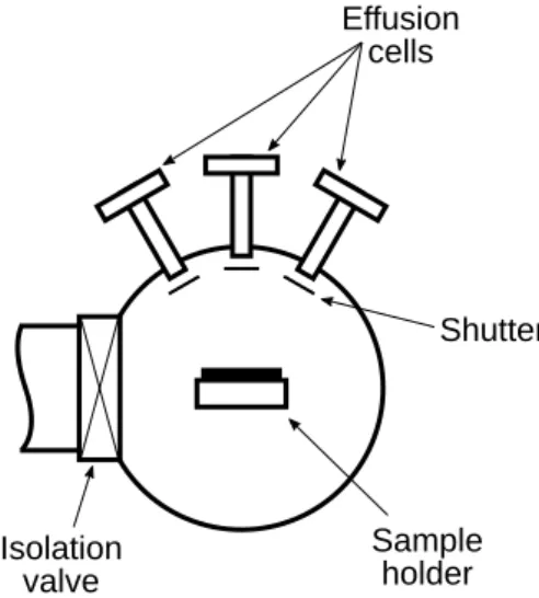
not require a high pressure, in fact a very low pressure is required, therefore this growing method must always be accompanied with a set ofUltra High Vacuum (UHV)chambers and pumps to allow the required low pressure, this low pressure is needed to ensure a clean surface of the substrate before any growth, ensure that the films grown are chemi-cally as pure as possible and to allow the molecular beam a high mean free path before hitting the substrate (otherwise the growth rate would be low).
Effusion cells
Shutter
Sample holder Isolation
valve
Figure 4.1: Some of the essential components that can be found on any MBE system.
As shown on the picture, aMBEsystem may contain more than one effusion cell, the
amount of these cells will depend on the desired film to be grown. The most common effusion cell used in these systems are Knudsen cells, these cells rely on low partial
pressure elements as a source for evaporation. These effusion cells evaporate the source
contained in a crucible often made of Pyrolytic Boron Nitride (PBN), quartz, tungsten or graphite [20], the material chosen for the crucible will dependent on what element source will be evaporated as well as the temperature at which the same source element will be evaporated. PBN crucibles are the industry standard for both GaN and GaAs crystal production [21], some of the properties that makePBN an attractive choice for these particular setups are [20,21]:
• Good thermal conductivity and stability
• High insulation resistance and dielectric strength over wide temperature range
• Material’s high purity and low outgassing
• Non-toxic and non-wetting
![Table 3.1: Raman active vibrational modes for wurtzite GaN [8].](https://thumb-eu.123doks.com/thumbv2/123dok_br/16546199.736945/45.892.131.772.258.452/table-raman-active-vibrational-modes-wurtzite-gan.webp)
![Table 4.1: Structural and thermal properties of SiC at room temperature [12].](https://thumb-eu.123doks.com/thumbv2/123dok_br/16546199.736945/48.892.119.768.825.1098/table-structural-thermal-properties-sic-room-temperature.webp)