DYNAMIC CHARACTERISTICS OF
IMPATT DIODES BASED ON WIDE
BANDGAP AND NARROW BANDGAP
SEMICONDUCTORS AT W-BAND
SOUMEN BANERJEE
Department of Electronics & Communication Engineering, Hooghly Engineering & Technology College Vivekananda Road, Pipulpati, Hooghly-712103, West Bengal, India
Abstract:
The properties and performance of p+pnn+ double drift Impatts based on Silicon, Indium Phosphide, 4H-Silicon Carbide and Si/Si1-xGex heterojunction have been investigated through modeling and simulation
technique at mm-wave window frequency of 94 GHz. The extensive simulation results reveal that 4H-SiC Impatt gives better performance both in terms of efficiency and output power as compared to its other counterparts. The conversion efficiency and output power obtained with wide bandgap semiconductor 4H-SiC based Impatt diode are 16.4 % and 35.104 W respectively at an optimum bias current density of 5 x 10⁸ A/m2 thus indicating its superiority over other Impatts. The design results presented in this paper are very encouraging and helpful to realize these diodes for mm-wave communication systems.
Keywords: Millimeter wave frequency, Homojunction, Heterojunction, Double Drift Impatt Diode, Wide band gap semiconductor.
1. Introduction
The W-band of millimeter wave Electro-magnetic spectrum ranges from 75-110 GHz. This band is used for millimeter wave radar research, military radar targeting and tracking applications and some non-military applications as well. The millimeter wave systems offer many advantages such as, smaller size, lighter weight, greater accuracy and resolution and smaller antenna size. The millimeter wave systems also provide greatly improved signal penetration through cloud, smoke and dust. The present day research activities for millimeter wave systems are centered on and around 35GHz and 94 GHz window frequencies where the atmosphere attenuation is found to be relatively low [Gasiewski and Klein, (2000)]. Even in the case of satellite, owing to the increasing spectrum and orbit congestion at lower frequencies, W-band satellite allocations are of increasing interest to commercial satellite operators’. The atmospheric radio window at 94 GHz is used for imaging, millimeter-wave radar applications in astronomy, defence and security applications.
The key element in millimeter wave transmitter systems is the solid state pulsed sources. These sources being small in size, light weighted and having a low voltage power requirement find applications as transmitters in many radar systems. Among several solid state sources, Impatts have emerged as the most promising and powerful source at microwave, millimeter–wave and sub-millimeter-wave frequencies. Impatts are widely used as solid state transmitters in tracking radars, missile seekers, radiometers and in various civilian, military and space communication sub-systems. The vast frequency range of operation and higher output power generation makes IMPATT a highly suitable device to meet the ever increasing communication needs of the world.
It is no secret that even today; Silicon dominates the micro-electronics industry owing to its low manufacturing cost and accounts for a lot of sales in the global semiconductor market. IMPATTs based on conventional silicon, are very popular and have already been fabricated at 94 GHz [Mukherjee and Banerjee, (2010)], [Dalle et al.,
higher electron saturation velocity, higher thermal conductivity, higher thermal stability and chemical inertness. However, SiC based IMPATTs are still in its developing stage, even though some reports are available in literature. Also, SiGe seems to play a major role in recent development of high speed optical networking and inexpensive, light-weight personal communication devices. SiGe devices have higher operating speed with lower electronic noise and lower power consumption. These devices support higher level of integration and thus enable the design of more functional components on chips. Thus the performance advantages of SiGe based devices lead to their choice for use and application in both wire integrated circuits and low power RF chips. Many parameters of Si1-xGex such as band gap, band offsets, effective masses, etc. are found to have strong strain dependence; the strain control thus becomes a vital necessity for any kind of band gap engineering conceivable in these materials. The advantage gained by the introduction of thin Si1-xGex films in their basic compatibility with standard silicon technology has made this heterostructure system an extremely interesting candidate for production devices. Si1-xGex (for x=0.6) heterostructure MITATTs based on Si have been fabricated [Luy et al., (1988)] and the CW power obtained is 25 mW with a conversion efficiency of 1.03 % at 103 GHz.
In the present paper, the authors have studied the performance of DDR Si, InP and 4H-SiC based homojunction and DDR Si/Si1-xGex based heterojunction Impatt diodes at 94 GHz window frequency. This is the first report on the comparative performance of Impatt diodes based on different materials at 94 GHz. The DC and high frequency performance of the devices are compared at optimum bias current density taking in to account the effect of mobile space charge. The avalanche response time and the transit time of the diodes which play a vital role in determining the device characteristics for high frequency performance are also investigated. The studies presented in this paper reveal the comparative performance of homojunction and heterojunction Impatt diodes which would provide the necessary design parameters for future realization of these devices.
2. Simulation Methodologies
2.1. Material parameters, design parameters and doping profile
2.2. Computer Simulation Techniques
The following assumptions are made in the computer analysis of DC and small signal behavior of double drift Impatt diodes; (a) One dimensional model of the p-n junction is treated; (b) The electron and hole velocities are taken to be saturated and independent of the electric field throughout the space charge layer.
DC Analysis of double drift Impatt diode
The computer simulation method starts with DC analysis described in details elsewhere [Pati et al., (1989)], [Banerjee et al., (1985)], [Roy et al., (1979)]. In this method the computation starts from the field maximum near the metallurgical junction. The distribution of DC electric field and carrier currents in the depletion layer is obtained by the double - iterative computer method, which involves iteration over the magnitude of field maximum (Em) and its location in the depletion layer. A computer algorithm has been developed for simultaneous numerical solution of Poisson’s equation, carrier continuity equations and the space charge equation taking into account the effect of mobile space charge and carrier diffusion in order to obtain the electric field profiles and carrier current profiles. The band gap energy of Si, InP and 4H-SiC are enlisted in Table-1. For Si1-xGex the band gap energy is expressed as Eg = 1.12-0.41x+0.008x2 at 300K for x<0.85 and the dielectric constant (static) of unstrained Si1-xGex layer grown on a <100> Si substrate is given by ε(x) = 11.7+4.5x at 300K [Schaffler et al., (2001)]. The electron and hole mobility of Si1-xGex is calculated from the method described elsewhere [Manku and Arokia, (1992)], [Manku et al., (1992)].
The carrier ionization rate have been computed using the relation
αn,p = An,p exp(-bn,p/E)m (1)
where E is the electric field; A nd B are the ionization coefficients. Repeated multiplication of charge carriers, like an avalanche, takes place by impact ionization in the high field region around a junction biased to breakdown. When a small reverse saturation electron or hole current enters either edge of the depletion layer of a reverse biased junction, the current is infinitely multiplied by the high field around the junction and the junction undergoes avalanche breakdown. The current multiplication factor is related to the ionization rates of charge carriers in the depletion layer and is given by
M
dx
W
1
1
0
(2)where
exp[
(
)
]
0
dx
xp n
n
; W = width of the depletion layer and M = current multiplication factor.Avalanche breakdown occurs in the junction when the electric field is large enough such that the charge
multiplication factors (Mn, Mp) become infinite. It is expressed as
1
0
dx
W
(3)If αn = αp = α, the breakdown condition is given by
1
0
dx
W
(4)The depletion layer of an Impatt diode is commonly divided in to a high-field avalanche region of width WA and low-field drift region of width WD. The avalanche zone width is customarily defined as
Figure – 1. Doping profile and Electric Field profile of p+
pnn+
95
.
0
0
dx
A W
(5)i.e., 95 % of the impact ionization takes place in avalanche zone. The breakdown voltage is calculated by integrating the spatial field profile over the total depletion layer width, i.e.,
2 1)
(
x
x
B
E
x
dx
V
(6)where –x1 = n – side depletion layer width; +x2 = p – side depletion layer width. Large number of charge carriers emerges from the avalanche zone and interacts with the field while crossing the drift zone. This interaction leads to the generation of high frequency oscillations.
The boundary conditions for the electric field at the depletion layer edges are given by
E (-x1) = 0 and E (+x2) = 0 (7) where -x1 and x2 define the p
+
and n+ edges of the depletion layer as shown in Fig. 2.
Figure – 2. Various parameters of Double drift p+
pnn+
Impatt diode
The boundary conditions for normalized current density P(x) = (JP – Jn)/J0 (where Jp =hole current density, Jn = electron current density) at the two edges are given by
P (-x1) = (2/Mp – 1) and P(x2) = (1 – 2/Mn) (8) The necessary device equations have been simultaneously solved [Pati et al., (1989)], [Banerjee et al., (1985)], [Roy et al., (1979)] satisfying the appropriate boundary conditions mentioned in equations (7-8). The field dependence of electron and hole ionization rates and saturated drift velocities of electron (vs,n) and holes (vs,p) at 300K are made use of in the computation for the profiles of electric field and carrier currents.
The conversion efficiency is calculated from the approximate formula [Scharfetter and Gummel, (1969)]
(%) = (1xVD) / ( x VB) (9)
where VD = Voltage drop across the drift region and VB = Breakdown voltage.
Small Signal Analysis of double drift Impatt diode
A W x sp snn
dx
dx
v
v
0exp[
0(
)
]
1
A W n pdx
0)]
(
exp[
simultaneously. The diode negative resistance (-ZR) and reactance (-Zx) are computed through numerical integration of the -R (x) and -X (x) profiles over the active space-charge layer.
Thus,
2 1 x x RRdx
Z
and
2 1 x x X
Xdx
Z
the diode impedance Zd is given by Zd = ZR + jZX and the admittance Yd is given by Yd = 1/Z = 1/( ZR + jZX) = G + jB. The real and imaginary parts of the diode admittance can be computed for various DC current densities and for different frequencies to obtain G-B plots.
The negative conductance (G), Susceptance (B) and the quality factor (Q) of the device can be calculated using the following relations:
-G = -ZR /[(ZR) 2
+ (ZX) 2
] and B =ZX / [(ZR) 2
+ (ZX) 2
] and -Qpeak = (B /-G)at peak frequency It may be noted that both –G and B are normalized to the area of the diode.
The avalanche frequency (fa) is the frequency at which the imaginary part (B) of the admittance changes its nature from inductive to capacitive. Again it is the minimum frequency at which the real part (G) of admittance becomes negative and oscillation starts to build up in the circuit.
The plot of negative resistance in the depletion layers of Impatt diodes show the relative contributions of various regions of the depletion layer to the high frequency power [Gummel and Blue, (1967)]. For double drift diodes, R(x) plots exhibit two maxima in the central part of the two drift layer with a minimum in the avalanche layer very close to the junction. For Si (in which αn > αp) DDR diodes, the maximum of R(x) in the electron drift layer exceeds that in the hole drift layer in magnitude; the opposite is the case for other material DDR diodes. It is also interesting to note that the avalanche region makes an appreciable contribution to the high frequency negative resistance.
At a resonant frequency of oscillation, the maximum power output PRF from the device can be obtained from the following expression,
PRF = V 2
RF (Gp) A/2 (10) where, VRF is the amplitude of the RF swing and is taken as VB/2, assuming 50% modulation of the breakdown voltage VB. Gp is the diode negative conductance at the operating frequency and A is the area of the diode, taken as 10-10 m2.
2.3.High Frequency limitation depending on Avalanche response time of Impatt diode
In most semiconductors the drift velocity increases linearly with electric field particularly at low-field range where the acoustic phonons are the main scattering agencies. However, at higher field values (E > 106 V/m) the dominant scattering is by optical phonons arising from high thermal vibrations of the lattice and the drift velocity of charge carriers saturate. Thus the transit time required by the charge carriers to cross the depletion region of the diode is proportional to the depletion layer width, since the velocity is constant at higher field range. The prime action underlying Impatt behaviour is Avalanche breakdown caused by a high electric field. There are various assumptions regarding this process manipulation as well as calculating the critical electric held. However, the main factor is the response time of the charged particles (electrons and holes) which is related to the avalanche multiplication and leads an important role in determining the device characteristics for high frequency performance.
If n and p be the response times for electrons and holes respectively, then these are expressed as
(11)
(12)
where and are the ionization coefficients; the expressions of and are expressed as
It is thus evident that both α and β are very strong functions of the electric field. For different semiconductor materials, the values of An, Ap, bn and bp at low electric field values and Ahn, Ahp, bhn and bhp at high electric field are calculated using the reported results in referred journals.
When avalanche is initiated by a mixture of electrons and holes then the corresponding response time 1 is given by
(13)
where k is the injection ratio, defined as Jps/Js and WA is the avalanche width. If the value of avalanche response time 1 is found to be smaller than the value of the transit time () of the materials, then only the diode can produce high frequency oscillation.
3. Results and Discussions
The material parameters of Si, InP, 4H-SiC and SiGe are enlisted in Table-1. At the design frequency of 94 GHz, the structural parameters of symmetrically doped Si, InP and 4H-SiC based homojunction DDR Impatt diode and Si/Si1-xGex (mole fraction x=0.1) based heterojunction Impatt diode are enlisted in Table-2. The DC and small signal analysis of the DDR diodes are carried out for different base materials which reveal that higher bias current can be passed through InP and 4H-SiC based Impatts as compared to Si and Si/SiGe Impatt diodes. The results indicate that Impatt based on 4H-SiC gives the highest power among all other Impatts at the same operating frequency.
The DC and small signal properties of the Impatts, obtained from simulation, at the optimum bias current density are shown in Table-3. The bias current is optimized with respect to highest conversion efficiency and highest output power. At 94 GHz window frequency, the peak electric field of Impatt diodes based on different materials lies in the range of 107-108 V/m. The peak electric field for 4H-SiC based DDR Impatt diode is found to be highest (3.61 x 10⁸ V/m) among Impatts based on other materials. Plots of peak electric field vs bias current density for the Impatts based on different materials are shown in Figure-3. This figure reveals that the peak electric field gradually decreases with the increase in bias current density. It is observed that 4H-SiC based Impatt has a very high breakdown voltage (212.4 V) as compared to 30.38 V for InP Impatt, 16.09 V for Si/SiGe Impatt and 18.00 V for Si Impatt at the same operating frequency of 94 GHz. Thus it is verified from simulation that the value of breakdown voltage obtained for WBG semiconductor 4H-SiC Impatt is found to be high owing to its greater band gap energy of 3.26 eV as expected. Plots of breakdown voltage vs bias current density are shown in Figure-4. The breakdown voltage also increases with increase in bias current density indicating a space charge induced positive resistance. The values of the space charge induced positive resistance evaluated from the slope of the plots in Figure-4 for Impatts based on Si, InP, 4H-SiC and Si/SiGe are 4 x 10⁻⁹
Ω/m2, 10 x 10-9Ω/m2, 15 x 10-9Ω/m2 and 2.75 x 10⁻⁹Ω/m2 respectively. The results reveal that a slight increase of current would lead to higher power in 4H-SiC Impatts as compared to Impatts based on other materials.
The conversion efficiency of Impatts based on different materials except Si is very high. The efficiency of heterojunction Si/SiGe Impatts and homojunction InP and 4H-SiC Impatts are found to be almost doubled as compared to homojunction Si Impatts. It is interesting to note that the efficiency of homojunction Impatt diodes increases significantly with the increase in the bandgap of the base semiconductor material. The conversion efficiency for Si DDR Impatt is found to be 8.92 % while the same for 4H-SiC, InP and Si/SiGe based Impatts are 16.4 %, 16 % and 14.82 % respectively. It is also interesting to note that Si/Si1-xGex heterojunction Impatt structure, made of two narrow bandgap semiconductors has significantly higher conversion efficiency as compared to those of homojunction Si Impatts. Plots of conversion efficiency vs bias current density for Impatt diodes based on different materials are depicted in Figure-5. The figure reveals that the conversion efficiency increases slowly with the increase of bias current density till the peak value is reached. Then it gradually decreases with further increase in bias current density.
Table-3 also gives the computed values of avalanche response time and transit time of the Impatt diodes at the design frequency of 94 GHz and at optimum bias current density. The avalanche response time in case of 4H-SiC Impatt is found to be 6.8 x 10⁻¹⁵ s and its corresponding transit time is obtained as 19.54 x 10⁻¹³ s at 94 GHz. For Si, InP and Si/SiGe based Impatts, the avalanche transit times are 5.1 x 10⁻¹³, 4.5 x 10⁻¹³ and 4.3 x 10 -12
s respectively and the corresponding transit times are 19.5 x 10⁻¹³, 2 x 10-12 and 57.9 x 10⁻¹³ s respectively. Hence at 94 GHz, the value of the avalanche transit time (1) is less than the transit time () for all the Impatt diodes, thereby clearly indicating that the diodes can produce oscillations at the designed mm-wave window frequency.
At 94 GHz, the peak negative conductances at the optimum bias current densities for homojunction DDR Impatt diodes are found to be 23.0 x 10⁶ S/m2, 79.54 x 10⁶ S/m2 and 6.225 x 10⁷ S/m2 for the base
1
0
1
[(
1
)
exp{
(
)
}]
AW
n
k
k
dx
semiconductors Si, InP and 4H-SiC respectively while the same for DDR Si/SiGe heterojunction Impatt diode is found to be 15 x 107 S/m2. The conductance-susceptance (G-B) plots for all types of Impatt diodes are shown in Figure-6. The G-B plots reveal that the optimum frequency corresponding to the peak value of negative conductance is close to the design frequency of 94 GHz, thereby, confirming the accuracy of the design..
The plots of negative resistance in the depletion layers of Impatt diodes, shown in Figure-7; indicate the relative contributions of various regions of the depletion layer to the high frequency negative resistance. For double drift diodes, the R(x) plots exhibit two peaks near the central part of the two drift layers with a dip in the avalanche layer very close to the junction.
The estimated output power from the device negative resistance is found to be 35.104 W for 4H-SiC Impatts at 94 GHz while the same for Si, InP and Si/SiGe Impatts are 0.093 W, 0.918 W and 0.480 W respectively at the same frequency. Thus heterojunction Si/Si1-xGex Impatts deliver higher power than homojunction Si Impatts. Thus from practical application point of view, Impatts based on 4H-SiC may be preferred owing to their capability of generating higher efficiency and much higher power than those generated by Si, InP and Si/SiGe Impatts at the design millimeter wave window frequency of 94 GHz. Plots of estimated output power vs frequency are depicted in Figure-8. The Q-factor determines the growth rate and stability of oscillation. A quality factor of 1.64, 4.00, 0.56 and 3.53 are obtained for Si, Si/Si1-xGex, InP and 4H-SiC Impatts. The results obtained are very encouraging and portrays the strong potentiality of homojunction Si, InP and 4H-SiC and heterojunction Si/SiGe Impatt diodes to be used as a powerful solid state source for communication systems at millimeter wave window frequency of 94 GHz. Also Impatts based on higher bandgap material like 4H-SiC is expected to be the future source of mm-wave communication systems.
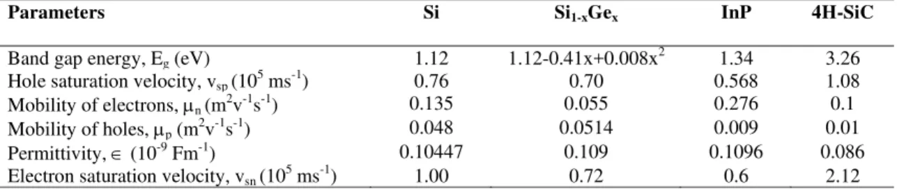
Table 1. Material parameters of Silicon, Silicon-Germanium, Indium Phosphide and 4H-Silicon Carbide
Parameters Si Si1-xGex InP 4H-SiC
Band gap energy, Eg (eV) 1.12 1.12-0.41x+0.008x
2
1.34 3.26
Hole saturation velocity, vsp (105 ms-1) 0.76 0.70 0.568 1.08
Mobility of electrons, n (m2v-1s-1) 0.135 0.055 0.276 0.1
Mobility of holes, p (m 2
v-1s-1) 0.048 0.0514 0.009 0.01
Permittivity, (10-9 Fm-1) 0.10447 0.109 0.1096 0.086
Electron saturation velocity, vsn (105 ms-1) 1.00 0.72 0.6 2.12
Table 2. Design parameters of double drift Impatt diodes at 94 GHz
Materials fD
GHz
|ND-NA|
m-3 J0 Am-2 Wp m Wn m W m
Si 94 2.5 x 10²² 0.5 x 10⁸ 0.350 0.350 0.700
Si/Si1-xGex 94 4.5 x 10²² 0.7 x 10⁸ 0.448 0.448 0.896
InP 94 17 x 1022 4.0 x 10⁸ 0.35 0.35 0.70
4H-SiC 94 35 x 1022 5.0 x 10⁸ 0.55 0.55 1.10
Table 3. DC and Small signal parameters of double drift Impatt diodes at 94 GHz
Parameters Si Impatt Si/Si1-xGex
Impatt
InP Impatt 4H-SiC Impatt
Design Frequency, fD (GHz) 94 94 94 94
Bias Current Density, J0 (A/m 2
) 0.5 x 10⁸ 0.7 x 10⁸ 4 x 10⁸ 5 x 10⁸
Peak Electric Field, Em (V/m) 4.39 x 10⁷ 3.21 x 10⁷ 7.35 x 10⁷ 3.61 x 10⁸
Breakdown voltage, VB (V) 18.00 16.09 30.38 212.4
Avalanche voltage, VA (V) 9.02 8.6 15.19 103.2
Efficiency, (%) 8.92 14.82 16.0 16.4
Avalanche response time, 1 (sec) 5.1 x 10
-13 4.3 x 10⁻¹² 4.5 x 10⁻¹³ 6.8 x 10⁻¹⁵
Transit time, (sec) 19.5 x 10⁻¹³ 57.9 x 10⁻¹³ 2.0 x 10⁻¹² 19.54 x 10⁻¹³ Peak negative conductance, Gp (S/m
2
) 38.13 x 10⁶ 15.0 x 10⁷ 79.54 x 10⁶ 6.225 x 10⁷
Quality factor, Q 1.64 4.00 0.56 3.53
(a). Si DDR Impatt diode (b). InP DDR Impatt diode
(c). 4H-SiC DDR Impatt diode (d). Si/SiGe DDR Impatt diode
Figure – 3. Plot of peak electric field vs bias current density for DDR Impatts at 94 GHz
(a). Si DDR Impatt diode (b). InP DDR Impatt diode
(a). Si DDR Impatt diode (b). InP DDR Impatt diode
(c). 4H-SiC DDR Impatt diode (d). Si/SiGe DDR Impatt diode
Figure – 5. Plot of efficiency vs bias current density for DDR Impatts at 94 GHz
(a). Si DDR Impatt diode (b). InP DDR Impatt diode
4. Conclusion
The simulation of the DC and high frequency properties of Si, InP and 4H-SiC homojunction double drift Impatt diodes and Si/SiGe heterojunction double drift Impatt diodes reveals that a much better performance in terms of
(a). Si DDR Impatt diode (b). InP DDR Impatt diode
(c). 4H-SiC DDR Impatt diode (d). Si/SiGe DDR Impatt diode
Figure – 7. Negative Resistivity Profiles of DDR Impatts at 94 GHz
(a). Si DDR Impatt diode (b). InP DDR Impatt diode
(c). 4H-SiC DDR Impatt diode (d). Si/SiGe DDR Impatt diode
output power and efficiency is observed with wide bandgap semiconductor 4H-SiC based Impatts at 94 GHz mm-wave window frequency. An efficiency of 16.4% and an output power of 35.104 W are observed at a bias current density of 5 x 10⁸ A/m2. Even though 4H-SiC Impatt is expected to be the superior candidate among Si, Si/SiGe and InP Impatts, the so far reported experimental results on 4H-SiC based Impatts are far from the expectations. This may be due to the fact that the device processing technology of 4H-SiC Impatts is complicated and needs further improvement to show satisfactory results. In this scenario, Impatt fabricated with Si/SiGe heterojunction structure may be preferred. However, the device results would be useful for practical realisation of Impatts based on all these materials and to compare their relative mm-wave properties and performances to be used as powerful solid state source of mm-wave power at W-band.
Acknowledgment
The author wish to thank Institute of Radio Physics & Electronics, University of Calcutta for the support of the research work.
References
[1] Gasiewski, A. J.; Klein, M. (2000): The sensitivity of Millimeter and Sub-millimeter frequencies to Atmospheric Temperature and Water Vapour variations. Journal of Geophysical Research – Atmospheres, 13, pp. 17481-17511.
[2] Mukherjee Moumita; Banerjee J. P. (2003): DDR pulsed Impatt sources at MM-wave window frequency: High power operation mode. Int. J. of Advanced Science and Technology, 19, pp. 1-12.
[3] Dalle, C.; Rolland, P.; Liete, G. (1990): Flat doping profile double drift Silicon Impatt for reliable CW high power high efficiency generation in the 94 GHz window. IEEE Trans. on ED, 37, pp. 227-236.
[4] Mukherjee, Moumita, et al. (2008): Millimeter wave properties of Photo-illuminated double drift InP Impatts at elevated temperature. Proc. of IEEE International Conference on Microwave and Millimeter wave Technology (ICMMT 2008), 2, pp. 897-900, China. [5] Buniatyan V. V.; Aroutiounian V. M. (2007): Wide gap semiconductor microwave devices. J. Phys. D, Appl. Physics, 40(20), pp.
6355-6385.
[6] Luy, J. F. et al. (1988): A Si/SiGe heterostructure MITATT diode. Electronics Letters, 24(22), pp. 1386-1387. [7] Electronic Archive: www.ioffe.ru/SVA/NSM/Semicond.
[8] Sze S. M.; Ryder R. M. (1971) : Microwave Avalanche Diodes. Proc. IEEE Special Issue on Microwave Semiconductor Devices. [9] Lee, J. et al. (1996): Responsivity and Impact ionization coefficients of Si1-xGex photodiodes. IEEE Trans on ED, 43(6), pp. 977-981. [10] Thomber, K. K., (1980): Relation of drift velocity of low field mobility and high field saturation velocity. J. Appl. Phys, 51, pp.
2127-2136.
[11] Manku Tajinder; Nathan Arokia (1992): Electron drift mobility model based on unstrained and coherently strained Si1-xGex grown on <100> silicon substrate. IEEE Trans. on ED, 39(9).
[12] Manku Tajinder et al. (1992): Drift hole mobility in strained and unstrained doped Si1-xGex alloys. IEEE Trans. on ED, 40(11). [13] Yeom K.; Hincley J. M.; Singh J. (1996): Calculation of electron and hole impact ionization coefficients in SiGe alloys. J. Appl. Phys,
80(12), pp. 6773-6782.
[14] Lin T. L. et al. (1991): SiGe-Si heterojunction internal photoemission long wavelength Infrared detectors fabricated by MBE. IEEE Trans. on ED, 38(5), pp. 1141-1144.
[15] Czajkowski K. et al. (1992): Impact ionization in GexSi1-x alloys and strained layers. J. Appl. Phys, 71(8), 3821-3826.
[16] Pati S. P.; Banerjee J. P.; Roy S. K. (1989): The distribution of negative resistivity in the active layer of Millimeter wave double drift region diodes. J. Appl. Physics, 22, pp. 959-964.
[17] Banerjee J. P.; Pati S. P.; Roy S. K. (1985): A Computer analysis of the distribution of high frequency negative resistance in the depletion layer of IMPATT Diodes. Proc. of Numerical Analysis of Semiconductor Devices and Integrated Circuits (NASECODE IV), Dublin, Ireland, pp. 494-498.
[18] Roy S. K.; Sridharan M.; Ghosh R.; Pal B. B. (1979): Computer method of the DC field and carrier current profiles in the Impatt devices starting from the field extremum in the depletion layer. Proc. of Numerical Analysis of Semiconductor Devices and Integrated Circuits (NASECODE I), Dublin, Ireland, pp. 226.
[19] Schaffler Friedrich (1997): High-mobility Si and Ge structures. Semicond. Sci. Technol., 12(12), pp. 1515-1549. [20] Scharfetter L.; Gummel H. K. (1969): Large signal analysis of a Silicon Read diode oscillator. IEEE ED, 16(1). [21] Gummel H. K.; Blue J. L. (1967): A small signal theory of avalanche noise in Impatt diodes. IEEE ED, 14, pp. 562.