Thermal evaporation furnace with improved configuration for growing
nanostructured inorganic materials
E. Joanni, R. Savu, L. Valadares, M. Cilense, and M. A. Zaghete
Citation: Rev. Sci. Instrum. 82, 065101 (2011); doi: 10.1063/1.3597577
View online: http://dx.doi.org/10.1063/1.3597577
View Table of Contents: http://rsi.aip.org/resource/1/RSINAK/v82/i6
Published by the AIP Publishing LLC.
Additional information on Rev. Sci. Instrum.
Journal Homepage: http://rsi.aip.org
Journal Information: http://rsi.aip.org/about/about_the_journal
Top downloads: http://rsi.aip.org/features/most_downloaded
Thermal evaporation furnace with improved configuration for growing
nanostructured inorganic materials
E. Joanni,1,a) R. Savu,2,3L. Valadares,4M. Cilense,2and M. A. Zaghete2
1Centro de Tecnologia da Informação Renato Archer – CTI, Rod. Dom Pedro I km 143.6, 13069-901, Campinas, SP, Brasil
2Departamento de Físico-Química, Instituto de Química de Araraquara, Universidade Estadual Paulista – UNESP, Rua Prof. Francisco Degni s/n, 14800-900, Araraquara SP, Brasil
3Centro de Componentes Semicondutores – CCS, Universidade de Campinas – UNICAMP, C.P. 6061, Rua João Pandia Calógeras, 90, 13083-870, Campinas, SP, Brasil
4Instituto de Química – UNICAMP, C.P. 6154, 13084-971, Campinas, SP, Brazil
(Received 8 November 2010; accepted 10 May 2011; published online 6 June 2011)
A tubular furnace specifically designed for growing nanostructured materials is presented in this work. The configuration allows an accurate control of evaporation temperature, substrate tempera-ture, total pressure, oxygen partial pressure, volumetric flow and source-substrate distance, with the possibility of performing both downstream and upstream depositions. In order to illustrate the versa-tility of the equipment, the furnace was used for growing semiconducting oxide nanostructures under different deposition conditions. Highly crystalline indium oxide nanowires with different morpholo-gies were synthesized by evaporating mixtures of indium oxide and graphite powders with different mass ratios at temperatures between 900oC and 1050oC. The nanostructured layers were deposited onto oxidized silicon substrates with patterned gold catalyst in the temperature range from 600oC to 900oC. Gas sensors based on these nanowires exhibited enhanced sensitivity towards oxygen, with
good response and recovery times.© 2011 American Institute of Physics. [doi:10.1063/1.3597577]
I. INTRODUCTION
For the last few years, progress in nanotechnology has led to the synthesis and characterization of a variety of nanos-tructures, i.e., nanowires, nanorods, nanotubes, using a wide range of materials such as metals,1 carbides,2 nitrides,3 and oxides.4 These nanometer-scale structures often possess en-hanced optical and electrical characteristics due to quan-tum confinement effects, as well as high surface-to-volume ratios,4,5 offering great prospects as building blocks in elec-tronic and photonic devices. Morphology, dimensions, unifor-mity, growth direction and cristallinity are crucial factors dur-ing the synthesis of nanostructures, as these parameters will ultimately dictate their functionality.4–6
Some of the methods more frequently reported for the synthesis of semiconducting oxide nanostructures, both in powder and thin film forms, include chemical bath deposition,7 hydrothermal synthesis,8 chemical vapor deposition,9 thermal evaporation,10,11 sputtering,12 and laser ablation.13
Among the physical deposition methods, the thermal evaporation (also called carbothermal reduction) is widely employed in nanofabrication processes due to its low cost, high yield, and easy implementation.6,10,11In spite of the pop-ularity of this technique, most of the results reported until now were not obtained through an accurate control of the deposi-tion process. The most common configuradeposi-tions used for ther-mal evaporation are either to locate the substrate at a certain distance from the source10 or to place the substrate over the
a)Author to whom correspondence should be addressed. Electronic mail:
ednan.joanni@cti.gov.br.
boat containing the raw materials.11 Both approaches have problems, since in the first case the substrate temperature is only approximately known (and includes a thermal gradient along the substrate) and, in the second one, the evaporation and deposition temperatures are the same. In both schemes the substrate temperature and source-substrate distance are not necessarily optimized or even compatible.
Works reporting the construction of vacuum furnaces with different configurations for attending a variety of re-search lines were already published.14–16 van Laake et al. designed and fabricated a simple, low-cost reactor based on resistive heating of a suspended silicon platform for carbon nanotube synthesis.15Their results are encouraging, with the possibility of expanding the use of the CVD furnace for other applications such as the anisotropic growth of semiconduct-ing oxides. However, the cost of buildsemiconduct-ing the reactor, as well as its maintenance, can be considered high for some research groups and the equipment demands delicate handling.
Schroeret al.developed two reactor designs for growing InAs nanowires.16Their hot wall reactor is based on a quartz tube furnace, being inexpensive and easy to mount and han-dle. Nevertheless, anisotropic growth can only be achieved for a narrow range of operating conditions. For improving nanostructure quality and increasing substrate coverage, the authors built a UHV cold wall reactor with a base pressure around 10−9Torr. On the other hand, this solution raised the
equipment costs to high levels, as acknowledged by the au-thors themselves.16
Having in mind that nanotechnology represents an im-portant research area and that the thermal evaporation method is one of the main techniques used for fabricating nanostruc-tures, a better controlled process is urgently needed in order
065101-2 Joanniet al. Rev. Sci. Instrum.82, 065101 (2011)
to achieve reproducible results that can be easily compared. In this work we report a new and simple configuration for the traditional thermal evaporation furnace that allows an accu-rate control of all the synthesis parameters. By adding a ce-ramic support that incorporates a substrate heater and a ther-mocouple, it becomes easy to set the desired evaporation and deposition temperatures and source-substrate distance. More-over, these parameters become independent from each other, considerably increasing the number of controlled variables and, consequently, improving the flexibility of the process. The system also allows the independent control of gas flow, composition, and pressure as well as the deposition of nanos-tructures either downstream or against the gas flow. Using this setup, highly crystalline semiconducting oxide nanowires with different morphologies were synthesized and their gas sensing properties were investigated.
II. EXPERIMENTAL DETAILS
A. Description of the evaporation system
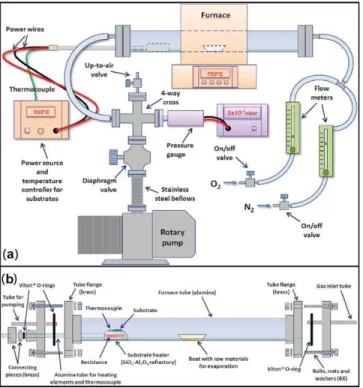
The complete system, shown in Fig.1(a), can be divided in two subsystems: one for atmosphere control and another for temperature management. The gas composition and flow are set by two volumetric flow controllers (one for oxygen and one for inert gases). The pressure is determined by a pressure sensor, diaphragm and up-to-air valves mounted in a 4-way cross and connected to a rotary vacuum pump. Tubes for gas introduction and pumping complete this subsystem. The con-figuration shown in Fig.1allows for downstream depositions; by reversing the tube placements, upstream depositions can also be performed. The evaporation is carried out in a tubular furnace with a single hot zone (EDG model FT-HV/20/10P)
FIG. 1. (Color online) Schematic drawings of (a) the complete system for growing oxide nanostructures by thermal evaporation and (b) the tube assem-bly and the substrate holder.
and equipped with a programmable temperature controller. A substrate holder provided with a separate heating system and temperature control allows the independent setting of evapo-ration and deposition temperatures.
Figure1(b)shows an schematic drawing of the alumina tube where the actual nanostructural growth takes place. The tube is fitted with brass flanges held in place with high tem-perature silicone-based adhesive. The mating flanges incorpo-rate inlet and outlet tubes for gas flow and a custom-designed coupling that allows the sample holder to be translated while maintaining a vacuum-tight connection. VitonR o-rings are
used for ensuring the hermetic sealing at all the interfaces. The sample holder was assembled from an aluminosilicate ceramic piece for supporting the substrates and an alumina tube of approximately 1 m length and 1.5 cm diameter having four through-holes for the thermocouple and electrical resis-tance connections. By using a single-zone furnace having a hot region of small dimensions when compared to the length of the tube, we were able to control the substrate temper-ature independently from the evaporation tempertemper-ature. This was achieved by varying the distance between the substrate holder and the center of the tubular furnace (i.e., between the substrate and the evaporation source). As a consequence, even though the furnace and substrate holder have their own controllers, the maximum difference between evaporation and deposition temperatures depends on the distance between the raw materials and the substrate. For example, if the source-substrate distance is too small, these temperatures will neces-sarily be similar.
In the process of building the substrate heater, a series of channels approximately 1 cm deep and 0.5 cm wide were excavated in the porous ceramic in order to accommodate the electrical resistance. The type K thermocouple and the con-nection wires for electrical supply of the Ni-Cr resistance were introduced inside the thin alumina tube. Subsequently, the ceramic piece was attached to this alumina tube using high temperature alumina cement. Next, the heater was coated with a thin cement layer in order to assure electrical insulation of the resistance, preventing also any chemical reaction with the evaporated materials.
B. System operation
The procedure for growing oxide nanostructures begins by loading the raw materials in a ceramic boat. The precur-sors are either metal granules, or mixtures of a finely ground oxide with a reducing agent (normally graphite). After placing the boat at the hot zone of the furnace, the substrates are po-sitioned on the sample holder, the distance between the boat and the sample holder is adjusted to the desired value, the flanges are closed and the tube is sealed by tightening the screws. At this point, the evaporation and deposition tempera-tures are set and both heaters are turned on. The vacuum pump is then started and the diaphragm valve is fully open in order to evacuate the tube up to its base pressure (5×10⁻²mbar
opened and the deposition pressure was adjusted by regulat-ing the diaphragm valve. When the deposition time was com-pleted, the heaters and the gas flow were turned off and the system was allowed to cool down.
C. Synthesis of semiconducting oxide nanowires and configuration of the gas sensors
By varying the source-substrate distance, the deposi-tion pressure, the gas flow, the percentage of oxygen and the substrate temperature, we were able to fabricate tin ox-ide nanowires, nano-plates, and nano-ribbons, indium oxox-ide nanowires and highly branched indium tin oxide nanowires. This demonstrates that the equipment is suitable for growing different inorganic materials in nanostructured form.
The procedure and results presented below refer to the growth of indium oxide nanowires using three source-substrate distances and four source-substrate temperatures, with all depositions being performed in the direction of the gas flow. Oxidized silicon, patterned with 160 nm thick gold catalyst dots, was used as substrates. The catalyst dots were deposited by DC sputtering through a shadow mask having an array of holes with a diameter of 172µm. Depositions of indium oxide nanostructures used as raw materials a mixture of indium ox-ide (In2O3– 99.9% purity, Alfa Aesar) and graphite powders.
Usually, the graphite is added to the oxide powder in order to lower its evaporation temperature. Using a rotary pump and volumetric flow controllers (between 100 and 200 sccm to-tal flow), an atmosphere composed of 90% N2 and 10% O2
or of pure nitrogen was employed and the deposition pres-sure was kept between 2 and 10 Torr. The source-substrate distance was adjusted between 8 and 13.5 cm, with the evap-oration time being varied in the range from 30 to 180 min. The deposition temperature, controlled independently of the evaporation temperature (900–1050oC), was varied between
600 and 900oC. The complete set of parameters used in this
work is presented in TableI.
After deposition, the degree of crystallinity and the phases present in the samples were analyzed by x-ray diffrac-tion (XRD – Rigaku Rint 2000), the growth direcdiffrac-tion of the nanostructures was studied by transmission electron mi-croscopy (TEM – Jeol JEM 2100), and their morphology was
TABLE I. Complete set of parameters used for the evaporation process of indium oxide nanowires.
Sample IE1 IE2 IE3 IE4 IE5
Indium oxide (g) 0.2 0.5 0.2 0.2 0.2
Graphite (g) 0.4 0.5 0.1 0.1 0.1
Source-substrate distance (cm) 13.5 10 8 8 8
Substrate temperature (oC) 600 900 625 700 700
Evaporation temperature (oC) 1000 1050 900 900 1000
Pressure(Torr) 7.5 2 10 10 10
N2flow (sccm) 180 180 90 100 100
O2flow (sccm) 20 20 10 . . . .
Evaporation time (min) 120 30 60 180 60
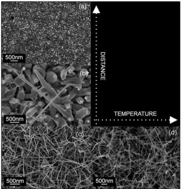
FIG. 2. FE-SEM surface images for the (a) IE1, (b) IE2, (c) IE3, and (d) IE4 indium oxide nanostructured films.
065101-4 Joanniet al. Rev. Sci. Instrum.82, 065101 (2011)
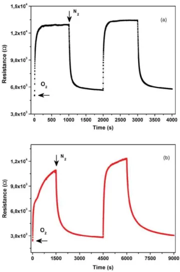
FIG. 4. (Color online) Gas sensing response towards oxygen for (a) the IE3 and (b) IE4 nanostructured gas sensors working at a temperature of 300◦C.
assessed by field emission scanning electron microscopy (FE-SEM – Zeiss Supra 35).
The sensitivity towards oxygen of the as-deposited sam-ples was tested at different working temperatures. This was possible due to the fact that the gold dots, besides their cat-alytic activity, also served as contact electrodes, making it possible to record the changes in resistance of the nanowires that bridged the gap between adjacent gold dots. For the elec-trical resistance measurements, the samples were maintained in nitrogen atmosphere (100 sccm N2) until the temperature
was stabilized; at this point the nitrogen flow was stopped, 100 sccm O2was injected into the chamber and the
measure-ments were started. The samples were submitted to four con-secutive oxygen/nitrogen cycles, using a working temperature of 300oC. The measurements were performed by means of an
electrochemical interface (Solartron 1287), applying a 0.5 V potential difference.
III. RESULTS AND DISCUSSION
Figure 2 presents surface FE-SEM images of the in-dium oxide nanostructured films as a function of the source-substrate distance and deposition temperature, sam-ples IE1 (Fig.2(a)), IE2 (Fig.2(b)), IE3 (Fig.2(c)), and IE4
(Fig. 2(d)). Decreasing the source-substrate distance from 13.5 to 8 cm, the film morphology changes from continu-ous dense layer (Fig. 2(a)), to large crystals with nanowires at their tips (Fig.2(b)) to a highly uniform nanowire array (Fig.2(c)). At a deposition distance of 13.5 cm, a dense layer was obtained, with no indication for nanostructural nucle-ation. This is mainly due to the low substrate temperature used for the deposition. For a source-substrate distance of 10 cm and a deposition temperature of 900oC, nanowires having a tip diameter of 100 nm with a very large base (Fig.2(b)) and a length of a few microns were grown. Their substrate cover-age density is low, and their size is not uniform. Furthermore, these nanowires are not preferentially oriented in relation to the substrate and their morphology indicates a large amount of liquid material during deposition. This is due to the low deposition pressure (2 Torr) and high evaporation and sub-strate temperatures (1050oC and 900oC, respectively). At this
evaporation temperature the vapor pressure of indium is∼5 ×10⁻² Torr, generating a larger amount of material arriving
on the substrate than for a deposition pressure of 10 Torr. All the nanowires have spheres at the tips indicating that under these conditions the growth mechanism is Vapor-Liquid-Solid (VLS). According to this mechanism, the nanowires grow by precipitation from droplets of super-saturated molten material present on the heated substrate surface.4,5,17 By decreasing the target-substrate distance to 8 cm and the substrate temper-ature to 625oC, morphologically uniform and interconnected
thin nanowires were obtained at a deposition pressure of 10 Torr (Fig.2(c)). Even for a low deposition temperature, by de-creasing the source-substrate distance, it is possible to trigger the nucleation and the growth of nanowires. The structures present widths of 30 nm and lengths of around 1µm. Very fine catalytic particles are still present at their tips, indicating the growing mechanism as being VLS. The substrate coverage density increased to approximately 76 wires/µm2. By
increas-ing the substrate temperature to 700oC the film morphology was not significantly affected. Nanowires with high substrate coverage and a diameter of 100 nm were obtained. Still, com-paring the IE3 and IE4 samples, one can observe that for the 700◦C deposition temperature the nanostructures are longer
in length, thinner and present catalytic particles with higher diameter at their tips. It is clear that this is due to the lack of oxygen during growth, leading to a higher amount of liquid phase at the substrate surface. Moreover, the deposition time for the IE4 sample was three times higher than for the IE3, resulting in a slight change in nanowire morphology.
reflect-ing the cubic crystalline structure of indium oxide. The SAED pattern taken perpendicular to the long axis of the nanowire (Inset Fig.3(b)), is consistent with the indexed patterns for the indium oxide with (100) growth direction.
Figure4shows the gas response towards oxygen for the IE3 (Fig.4(a)) and IE4 (Fig.4(b)) sensing devices. For the working temperature of 300oC, the IE3 sensor exhibits a good reproducibility and a high stability for the four gas cycles per-formed. The sensibility (defined as the ratio between the re-sistance in O2 and the resistance in N2) for this device is of
2.5 for the testing temperature used, with response and re-covery times (defined as 90% of the final value in O2 and
N2 atmospheres, respectively) of 1 and 3 min, respectively.
Even though its sensibility is reasonable, the IE4 gas sensor presents a very slow response, not stabilizing for the same time interval used for testing. Moreover, its recovery is very slow, requiring more then double the testing time used for the IE3 sensing device. As the device does not stabilize in any of the gases used, the response and recovery times could not be determined. The initial low resistance of these devices can be due to the continuous layer at the base of the nanostructures that acts as a thin sensing film and contributes to the final sensing response.
IV. CONCLUSIONS
In this work we report the design and assembly of an evaporation furnace with improved configuration. By using a better control of the deposition parameters, nanostructures with different morphologies were obtained. The FE-SEM im-ages of the indium oxide nanowires show that the structures grow either by VLS or VS mechanism, depending on the pro-cessing conditions. The TEM analysis indicated their high degree of cristallinity, with no grain boundaries along their length. The gas sensing devices based on these nanostructures shows good sensibility towards oxygen at a working temper-ature of 300oC. The relatively short response time and good reproducibility of some of the gas sensors indicate that, with a controlled and low cost system, devices with high perfor-mance can be obtained.
The main contribution of this work is, to the best of our knowledge, the possibility to control, for the first time, all the major parameters involved in the growth of oxide
nanostructures by evaporation. Furthermore, variables which normally are interdependent (pressure and gas flow, evapora-tion temperature, and deposievapora-tion temperature) become inde-pendently controllable. Other advantages of such evaporation system are the simple assembly, operational flexibility and low cost. The system offers good reproducibility, even for a large range of operation conditions, allowing the fabrication of nanostructures with different morphologies.
ACKNOWLEDGMENTS
R. Savu would like to acknowledge the financial sup-port of FAPESP Brazilian foundation through her Ph.D. grant (Grant No. DD05/59270-0). All the authors acknowl-edge the financial support of FAPESP and CNPq Brazilian foundations.
1L. Chen, K. Arakawa, and H. Mori, Nanotechnology 21, 285304 (2010).
2M. Yamaguchi, S. Ueno, R. Kumai, K. Kinoshita, T. Murai, T. Tomita, S. Matsuo, and S. Hashimoto,Appl. Phys. A99, 23 (2010).
3M. U. Niemann, S. S. Srinivasan, A. R. Phani, A. Kumar, D. Y. Goswami, and E. K. Stefanakos,J. Nanomater.2008, 950967 (2008).
4S. V. N. T. Kuchibhatla, A. S. Karakoti, D. Bera, and S. Seal,Prog. Mater.
Sci.52, 699 (2007).
5J. G. Lu, P. Chang, and Z. Fan,Mater. Sci. Eng. R52, 49 (2006). 6Z. R. Dai, Z. W. Pan, and Z. L. Wang,Adv. Funct. Mater.13, 9 (2003).
7B. Cao and W. Cai,J. Phys. Chem. C112, 680 (2008).
8U. Pal and P. Santiago,J. Phys. Chem. B109, 15317 (2005).
9Y. Hao, G. Meng, C. Ye, and L. Zhang,Cryst. Growth Des. 5, 1617 (2005).
10Z. R. Dai, Z. W. Pan, and Z. L. Wang,J. Am. Chem. Soc.124, 8673 (2002).
11H. Jia, Y. Zhang, X. Chen, J. Shu, X. Luo, Z. Zhang, and D. Yu,Appl. Phys.
Lett.82, 4146 (2003).
12K. W. Cheng, Y. T. Lin, C. Y. Chen, C. P. Hsiung, J. Y. Gan, J. W. Yeh, C. H. Hsieh, and L. J. Chou,Appl. Phys. Lett.88, 043115 (2006).
13R. Savu and E. Joanni,J. Mater. Sci.43, 609 (2008).
14C. C. Lee, D. T. Wang, and W. S. Choi,Rev. Sci. Instrum.77, 125104 (2006).
15L. van Laake, A. J. Hart, and A. H. Slocum,Rev. Sci. Instrum.78, 083901 (2007).
16M. D. Schroer, S. Y. Xu, A. M. Bergman, and J. R. Petta,Rev. Sci. Instrum.
81, 023903 (2010).
17P. Cheyssac, M. Sacilotti, and G. Patriarche,J. Appl. Phys.100, 044315 (2006).
18E. Comini, C. Baratto, G. Faglia, M. Ferroni, A. Vomiero, and G. Sberveg-lieri,Prog. Mater. Sci.54, 1 (2009).