155
PACS numbers: 61.46.Bc, 68.37.Og, 78.30.Ly 78.67.Hc, 81.07.Bc
A STUDY OF THE EVOLUTION OF THE SILICON
NANOCRYSTALLITES IN THE AMORPHOUS SILICON CARBIDE UNDER ARGON DILUTION OF THE SOURCE GASES
A. Kole, P. Chaudhuri
Energy Research Unit, Indian Association for the Cultivation of Science, Jadavpur, Kolkata – 700032
E mail: [email protected]
Structural evolution of the hydrogenated amorphous silicon carbide (a-SiC:H) films deposited by rf-PECVD from a mixture of SiH4 and CH4 diluted in Ar shows that a smooth transition from amorphous to nanocrystalline phase occurs in the material by increasing the Ar dilution. The optical band gap (Eg) decreases from 1.99 eV to 1.91 eV and the H-content (CH) decreases from 14.32 at% to 5.29 at% by increasing the dilution from 94 % to 98 %. at 98 % Ar dilution, the material contains irregular shape Si nanocrystallites with sizes over 10 nm. Increasing the Ar dilution further to 98.4 % leads to a reduction of the size of the Si nanocrystals to regular shape Si quantum dots of size about 5 nm. The quantum confinement effect is apparent from the increase in the Eg value to 2.6 eV at 98.4 % Ar dilution. Formation of Si quantum dots may be explained by the etching of the nanocrystallites of Si by the energetic ion bombardment from the plasma.
Keywords: SILICON CARBIDE, RF- PECVD, AR DILUTION, OPTICAL BAND GAP,
SI QUANTUM DOTS, QUANTUM CONFINEMENT.
(Received 04 February 2011)
1. INTRODUCTION
Study of the formation of silicon quantum dots (Si q-dots) which are silicon nanocrystallites having sizes of the order of Bohr atomic radius ( 5nm) embedded in high band gap amorphous oxides, nitrides or carbides of silicon is highly interesting from the point of view of understanding the basic physics of the interaction of the light quanta with such quantum size matter. Tuning of the band gap in these materials by controlling the size of the Si q-dots have possible technical application in photoluminescent devices and in for third generation solar cells.[1, 2] Most of the works on Si q-dots in a-SiC matrix used hydrogen dilution of the source gases containing Si and C.[3] In this paper we are reporting our studies on the gradual evolution of the nanocrystalline Si into Si quantum dots in a-SiC:H films by the control of the argon dilution of the source gases.
2. EXPERIMENTAL
No. (sccm) (sccm) (sccm) ( C) (Torr) (mW/cmdensity 2)
#QD1 3 3 94 200 0.2 400
#QD2 2 2 96 200 0.2 400
#QD3 1.5 1.5 97 200 0.2 400
#QD4 1 1 98 200 0.2 400
#QD5 0.8 0.8 98.4 200 0.2 400
3. RESULTS
3.1 XRD
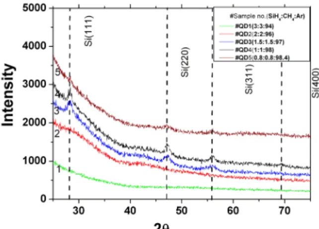
No diffraction peak related to crystalline silicon is observed up to a dilution level of 96 % (Curves 1 and 2, Fig. 1). But at 97 % dilution of Ar small, broad but clearly resolved diffraction peaks at 2 28.4 , 47.3 , and 56.1 appear corresponding to the (111), (220), and (311) crystal planes of silicon res-pectively (Curve 3, Fig. 1).[4, 5] With further increase of the dilution level to 98 %, the intensities of all three diffraction peaks are increased while the full widths at half maximum (FWHM) of all these diffraction peaks become smaller [Curve 4, Fig. 1]. An additional peak at 69.2 corresponding to (400) plane of Silicon also appears at this dilution level. The peaks however, becomes broad when the Ar dilution level is further increased to 98.4 % (Curve 5, Fig. 1).
3.2 Optical band gap
The optical absorption of the films were measured by UV-Vis spectroscopy to study the optical band gap of the materials. The band gap was obtained from the commonly used Tauc’s formula (equation 1),
( h )0.5 B(h – E
g), (1)
Fig. 1 – XRD pattern of the films deposited under different dilution levels of Ar
Fig. 2 – Tauc’s plot of the a-SiC:H samples deposited at different ar dilution
3.3 FTIR
The nature of the Si-C, Si-H and C-H bonds within the samples deposited at different dilution level of Ar studied by FTIR absorption spectroscopy are shown in Fig. 3. These spectra have been corrected for the substrate absorption and normalized by the film thickness. The main absorption peaks appearing in the spectra are located at (1) ~ 650cm – 1 , (2) ~ 780 cm – 1, (3) ~ 1000 cm – 1, (4) 1900 - 2100 cm – 1 and (5) 2800 - 3100 cm – 1.These peaks are attributed to (1) the wagging or rocking mode of Si-Hn for n 1 - 3, [8], (2) the stretching mode of Si-C, [9], (3) the wagging or rocking mode of C-Hn [10, 11], (4) the stretching mode of Si-H [12] and (5) stretching modes of C-Hn (sp3) or C-Hn(sp2) for n 1 - 3 [13] respectively. With the increase in Ar dilution level the intensities of the peaks at ~ 650 cm – 1 and ~ 2090 cm – 1 related to Si-H bond decrease. This phenomenon may be associated with the nanocrystalline Si formation in the amorphous matrix. [14] It is also observed that the peak at ~ 1000 cm – 1 and the absorption band between 2800 -3100 cm – 1 (both related to C-H
Fig. 3 – FTIR absorption spectra of the films grown at different Ar dilution
3.4 HRTEM
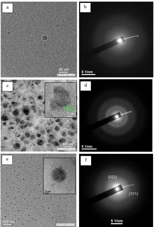
At 94% Ar dilution amorphous nature of a-SiC:H films is apparent from the featureless micrograph (See Fig. 4a). Corresponding SAED (Fig. 4b) shows diffused hallow pattern. With the increase in Ar dilution level diffused rings appear in the SAED indicating formation of the nanocrystallites. The micrograph and the SAED for the 98 % diluted sample are shown in Fig. 4c, d. The micrograph shows randomly oriented nanocrystalline Si of variable sizes. The fringe pattern corresponding to (111) plane of silicon is clearly discernible in the micrograph (Fig. 4c inset). The SAED (Fig. 4d) also shows a sharp ring corresponding to this plane. At 98.4 % Ar dilution the micrograph consists of uniformly distributed nanocrystals of size ~ 5 nm Fig. 4e). A distinct feature is observed in the SAED of this film showing a diffused ring with some spots on it. The distinct spots coincide with the Laue spots for the planes (220) and (311) of Si. This unique feature may have appeared in the diffraction pattern when the size of the nanoparticle is reduced to the size of the order of Bohr radius producing the Si quantum dots in the dielectric matrix of SiC.
4. DISCUSSIONS
Fig. 4 – HRTEM images of the samples deposited at different Ar dilution. (a), (c), (e) shows the bright field micrograph of the samples deposited at 94 %, 98 % and 98.4 % respectively. (b), (d) and (f) shows the corresponding selected area electron diffraction (SAED) pattern of the samples for 94 %, 98 % and 98.4 % Ar dilution levels respectively
a b
c d
Fig. 5 – Changes in CH, E04 and Eg with Ar dilution
Argon takes leading role in the dissociation of SiH4 and CH4 in the plasma as also influencing the surface reactions. While the Ar+ ions have higher reaction rate with CH4, the neutral metstable Ar* is chiefly responsible for the dissociation of SiH4. Thus presence of the relative amounts Ar* and Ar+ in the plasma determines the dissociation of SiH
4 and CH4. Moreover, bombardment of the growth surface by Ar+ and Ar* influences the surface reactions which is important for the evolution of the deposited from amorphous to nanocrystalline phase. Diffused rings containing Laue spots have been observed in the case of Si quantum dots formed within porous silicon [15].
With increasing Ar dilution the growth of amorphous to micro/nano-crystalline silicon occurs through the more and more bombardment of the growth surface by the metastable Ar* atoms and Ar+ ions from the plasma. Energy transferred to the surface increases the mobility of the surface adatoms helping in the formation of the nanocrystallites [16]þAt higher Ar dilution the momentum transfer to the surface causes etching from the surface. The nanocrystallites are also etched and their size reduced to form silicon quantum dots.
5. CONCLUSION
We have observed that deposition of quantum dots of uniform and regular size in a-SiC:H matrix occurs through the etching out of the initially formed larger size and irregularly shaped nanocrystallites of silicon. Bombardment of the growth surface by the ions from the plasma has been proposed to play a major role in the etching process.
REFERENCES
1. S.M. Kang, S.G. Yoon, S.W. Kim, and D.H. Yoon, J. Nanosci. Nanotechno. 8 3857 (2008).
2. G. Conibeer, M. Green, R. Corkish, Y. Cho, E.-C. Cho, Chu-W. Jiang, T. Fangsuwan-narak, E. Pink, Y. Huang, T. Puzzer, T. Trupke, B. Richards, A. Shalav, K.-L. Lin, Thin Solid Films511,654 (2006).
3. Y. Kurokawa, S. Tomita, S. Miyajama, A. Yamada, M. Konagai, Jap. J. Appl. Phys.46 L833 (2007).
4. Q.J. Cheng, S. Xu, S.Y. Huang, K. Ostrikov, Cryst. Growth Des. 9 2863 (2009). 5. Y. Hotta, H. Toyoda, H. Sugai, Thin Solid Films515 4983 (2007).
6. Q.J. Cheng, S. Xu, K. Ostrikov, J. Phys. Chem. C113 14759 (2009). 7. Q.J. Cheng, S. Xu, K. Ostrikov, J. Mater. Chem. 19 5134 (2009). 8. M.H. Brodsky, M. Cardona, J.J. Cumo, Phys. Rev.B16,3556 (1977). 9. Y. Catherine and G. Turban, Thin Solid Films60 193 (1979).
10.H. Wieder, M. Cardona, and C.R. Guarnieri, phys. status solidi B92, 99 (1979). 11.W. Yu, X. Wang, W. Lu, S. Wang, Y. Biana, G. Fu, Physica B 405 1624 (2010). 12.A. Bhaduri, A. Kole, P. Chaudhuri, phys. status solidi C7,774 (2010).
13.Q. Cheng, E. Tam, S. Xu, K. Ostrikov, Nanoscale 2, 594 (2010). 14.A. Chowdhury, S. Ray, phys. status solidi C7, 628 (2010).