986 Brazilian Journal of Physics, vol. 36, no. 3B, September, 2006
Adherent Diamond-Like Carbon Coatings on Metals Via PECVD and IBAD
Gil Capote∗, Lu´ıs F. Bonetti∗,†, L´ucia V. Santos∗, Vladimir J. Trava-Airoldi∗, and Evaldo J. Corat∗
∗Laborat´orio Associado de Sensores e Materiais, Instituto Nacional de Pesquisas Espaciais,
Caixa Postal 515, 12245-970, S˜ao Jos´e dos Campos - SP, Brazil
†Instituto Tecnol´ogico de Aeron´autica, Centro T´ecnico Aeroespacial, S˜ao Jos´e dos Campos - SP, Brazil
Received on 8 December, 2005
Adherent and low-stress a-C:H films were deposited on Ti6Al4V and stainless steel substrates using PECVD and IBAD techniques. An amorphous silicon interlayer was applied to improve the adhesion of the a-C:H films on the metal substrates. The XPS technique was employed to analyze the chemical bondings within the interfaces. The elemental composition and atomic density of the films were determined by ion beam analysis. The film microstructure was studied by means of Raman scattering spectroscopy. The mechanical properties were determined by means of stress and hardness measurements. The adherence was evaluated by means of scratch tests. The tests showed that the composition, the microstructure, and the mechanical properties of the films depend on the intensity of the ion bombardment and on the ion current.
Keywords: Diamond-like carbon; Plasma enhanced chemical vapor deposition; Ion beam-assisted deposition
I. INTRODUCTION
Research and development of nanostructured carbon-based coatings with tailor-designed properties is a fundamental need for the automotive, aerospace, biomedical and electronic in-dustries. The amorphous hydrogenated carbon (a-C:H) fam-ily of films stands out due to their properties of high hardness, chemical inertness, low friction and high-wear resistance. The major disadvantage of super hard diamond-like carbon (DLC) film deposition and, therefore, their technical applications is that there is often a relatively low adhesion of these films on metallic substrates caused by very high total compressive stress on these coatings. To overcome the low adhesion prob-lems of these films on metallic substrates, different coating concepts have been proposed by many research groups, such as: deposition of a thin metal interlayer [1-2]; surface implan-tation [3]; chemical interlayer gradients or a multilayer coat-ing [4]; variation of the self-bias voltage in the beginncoat-ing of the deposition [5]; and use of surface thermal treatments [6]. The interlayers, especially the multilayers, cause a continual change in the thermal expansion coefficient and help to reduce stress in the a-C:H films.
DLC film deposition can be accomplished economically at low temperature, utilizing plasma enhanced chemical va-por deposition (PECVD) techniques, sputtering methods, arc-discharge, pulsed laser deposition (PLD), and ion beam-assisted deposition (IBAD) techniques [7]. The adherent and low-stress a-C:H films are mostly produced by plasma decom-position of a hydrocarbon-containing precursor atmosphere using PECVD methods. Different silicon precursors have been applied to deposit a thin silicon interlayer between metal-lic substrates and a-C:H films in order to increase adherence of the coatings [1,2,8]. The IBAD, a combination of ion implan-tation and physical vapor deposition, can utilize energetic ion bombardment to enhance the films’ adhesion on metals and to deposit the films at low substrate temperature. The IBAD process probably offers the only means to deposit DLC films onto steels and others metal substrates with particularly good interface adhesion [9-11].
In this study, both PECVD and IBAD systems were used to deposit adherent and low-stress a-C:H films on Ti6Al4V and stainless steel substrates. A thin amorphous silicon interlayer was used to improve the a-C:H films’ adhesion. The films deposited via PECVD and IBAD were analyzed according to their microstructure, mechanical and tribological properties as a function of self-bias voltage and ion current.
II. EXPERIMENTAL PROCEDURES
DLC films were deposited by the PECVD and the IBAD methods, employing an asymmetrical capacitively-coupled deposition system [7] and end-Hall ion source [11], re-spectively. The thin amorphous silicon interlayers (10-100 nm) were deposited only by the PECVD technique, which uses silane as the precursor to improve the film’s adhesion. Ti6Al4V alloy and stainless steel 304 substrates were pol-ished by using up to 0.25 microns of diamond powder and were cleaned ultrasonically in an acetone bath before putting them into a vacuum chamber. The substrates were addition-ally cleaned in argon discharge prior to deposition. In addi-tion, Si (100) substrates were used in order to measure the total stress of the a-C:H films. The films obtained by r.f. PECVD were deposited with a total gas pressure of 10.5 Pa at 5 and 10 sccm gas flows for silane and methane, respec-tively. The self-bias voltage was varied from 0 up to -500 V according to growth parameters by adjusting the r.f. power input for both silicon and DLC films.
In the IBAD method, argon was used as the bombard-ment gas, while methane was used as a precursor. The ar-gon/methane rate was kept constant at 1/4, while the ion en-ergy was maintained constant at 150 eV. The operating pres-sure in the chamber was approximately 3x10⁻⁴Pa. A series of DLC films were deposited by changing the ion current from 2 up to 4.5 A. Film thickness in the range of approximately 2 µm was determined by stylus profilometry.
us-Gil Capote et al. 987
ing a surface Kratos XSAM HS instrument with monochro-matic Al Kα line of an X-ray source with energy of 1486.6 eV and 168 W of power. The measurements were taken in an ultra-high vacuum environment. Binding energy positions were verified using the C 1s peak at 284.8 eV, which was asso-ciated to C-C and/or C-H bindings. The peaks were adjusted using Gaussian curves and the background was approximated by the Shirley method.
FIG. 1: Deposition rate as a function of the Vband of the Icfor films
deposited by PECVD and IBAD, respectively.
The elemental composition was determined by ion beam analysis (IBA), using Rutherford backscattering spectrome-try (RBS) and elastic recoil detection analysis (ERDA) to de-termine the relative concentration of hydrogen, employed a 1.6-MV Pelletron electrostatic accelerator 5SDH from the Na-tional Electrostatic Corporation. For the measurements, a 2.2-MeV He+beam was used. The atomic density was inferred by combining the atomic density of the area provided by IBA and the film thickness.
The film’s atomic arrangements were analyzed by Raman scattering spectroscopy. The spectroscopy was performed with a Renishaw 2000 system using an Ar+-ion laser (λ = 514 nm) in backscattering geometry. The laser power on the sample was∼0.6 mW and the laser spot had a 2.5µm
diame-ter. The Raman shift was calibrated in relation to the diamond pick at 1332 cm−1. All measurements were carried out in air at room temperature.
Total stress was determined by measuring the film curva-ture by means of stylus profilometry and by applying Stoney’s
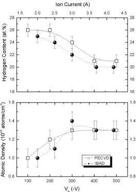
FIG. 2: The hydrogen content and atomic density of the a-C:H films as functions of the Vband of the Ic.
equation [12]. The hardness of the films was measured by employing a Fisherscope micro indenter, applying a load of 20 mN. The values presented in this study correspond to the average of 13 indentations.
Micro-scratch tests were used to evaluate the film adher-ence, using a conical tip, 200 µm radius, diamond stylus (Rockwell C 120o). The normal force was kept constant for each test at 5, 10, and 20 N.
III. RESULTS AND DISCUSSIONS
From XPS spectra, the presence of C 1s, O 1s, Si 2s and Si 2p peaks were observed. Oxygen may have been incor-porated into the films from residual water pressure inside the chamber and from the film’s exposure to the laboratory at-mosphere. The results suggest that SiC (∼25% of the silicon
peak) formed in the interface between the amorphous silicon interlayer and DLC films. This chemical bonding is strong and it is probably responsible for the good DLC film adher-ence on the silicon layer. Most of the silicon appeared in metallic form (Si0) (∼55%), which is probably responsible
for the silicon binding with the metallic substrate. In the DLC films, C-C and C-H bindings predominated (∼70%). This
re-sult was expected since these chemical bondings are the ma-jority in a-C:H films.
988 Brazilian Journal of Physics, vol. 36, no. 3B, September, 2006
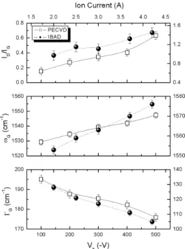
FIG. 3:ID/IGintensity ratio, G band peak position (ωG)and G
band-width (ΓG)as a function of the Vband Ic.
films deposited by PECVD and IBAD, respectively. In both cases, increases in the deposition rates were observed. This behavior can be explained by the higher power input needed to achieve the desired self-bias voltage and consequently, the more efficient plasma dissociation. Films deposited by IBAD method needed, on the other hand, a higher methane flow to obtain the higher values of the ion current. Higher intensity ion bombardment may have contributed to the increased num-ber of absorption sites.
The hydrogen content and atomic density of the a-C:H films as a function of the Vb and of the Ic are presented in Fig. 2. In both cases, the films deposited at low Vb and Ic pre-sented higher hydrogen contents and lower atomic densities, while for higher Vband Icvalues, the density increased and hydrogen content decreased. The hydrogen content and the atomic density kept approximately constant values (21 at.% and 1.3x10²³ atoms/cm3, respectively). These values corre-spond to what are typically reported in the literature for a-C:H films [7]. This behavior is due to a more energetic ion bombardment, leading to preferential hydrogen sputtering that occurs because of the weaker strength of C-H bonds when compared to the C-C bonds. Moreover, greater CH4
mole-cule fragmentation in the plasma as the power was increased may have contributed to the decrease of the incorporation of hydrogen.
The Raman spectra for a-C:H films presented two overlap-ping bands known as D and G bands, which appear approx-imately at 1390 cm−1 and at 1545 cm−1, respectively. The
spectra can be fitted using two Gaussian lines. The ID/IG intensity ratio, G band peak position (ωG)and G bandwidth (ΓG)as a function of the Vband Ic, obtained from the fitted
parameters, for films deposited by both techniques are plot-ted in Fig. 3. The increase of theID/IGratio, together with the shift of theGband’s peak position towards higher frequencies, accompanied by a reduction of the bandwidth, is usually in-terpreted in terms of an increase of graphitic domains, either in number or in size [13]. The results suggest a progressive graphitization of the a-C:H films upon self-bias and ion cur-rent increases.
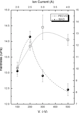
Figures 4 and 5 present the total compressive stress and the hardness values as functions of the self-bias voltage and of the ion current, respectively. In Fig. 4, the stress measurements for a-C:H films deposited by PECVD directly on Si(100) sub-strate, on metallic substrate with amorphous silicon interlayer, and for films deposited by IBAD are presented. A significant decrease of the stress values was observed when the a-C:H films were deposited using a silicon interlayer. This result suggests that internal stress reduction is responsible for the in-crease of a-C:H film adherence on metallic substrates. Also, a significant decrease of the stress values for the film deposited by IBAD was observed. Both the internal stress and hardness values reached a maximum. The existence of this maximum in a-C:H films has been explained by the subplantation model [14]. The stress and hardness reduction in the films deposited with higher Vband Icsuggests a progressive graphitization, as had been observed in the Raman results.
FIG. 4: Total compressive stress as a function of the Vb and Icfor
films deposited by both techniques.
Gil Capote et al. 989
FIG. 5: Hardness as a function of the Vb and Ic for a-C:H films
deposited by PECVD and IBAD techniques.
IV. CONCLUSION
The use of the thin amorphous silicon interlayer enhanced the deposition of adherent, low-stress a-C:H films on Ti6Al4V and stainless steel substrates via PECVD. The Vbfor PECVD and Icfor IBAD techniques play a similar role in term of to-tal stress, hardness, and adherence studies. Analysis of DLC film showed that the composition, the microstructure, and the mechanical properties of these films depend on the intensity of ion bombardment and on the ion current.
A comparison of the results obtained with the PECVD and the IBAD techniques shown the similar results for the depo-sition rate, hydrogen content, atomic density, and Raman pa-rameters. A decrease of the total compressive stress and of the hardness values were observed in the films deposited by IBAD method.
Acknowledgement
This study was supported by FAPESP and CNPq.
[1] V. Bursikova, V. Navratil, L. Zajickova, and J. Janca, Mater. Sci. Eng. A324, 251 (2002).
[2] S. Takeuchi, A. Tanji, H. Miyazawa, and M. Murakawa, Thin Solid Films447-448,208 (2004).
[3] C.S. Lee, T.Y. Kim, K.R. Lee, and K.H. Yoon, Thin Solid Films 447-448, 169 (2004).
[4] Q.R. Hou, J. Gao, Appl. Phys. A68(3), 343 (1999).
[5] S. Zhang, X.L. Bui, Y. Fu, D.L. Butler, and H. Du, Diamond Relat. Mater.13, 867 (2004).
[6] P. Mosaner, M. Bonelli, and A. Miotello, Appl. Surf. Sci. 208-209, 561 (2003).
[7] J. Robertson, Mater. Sci. Eng. R37, 129 (2002).
[8] Y. Jun, J.Y. Choi, K.R. Lee, B.K. Jeong, S.K. Kwon, and Ch.H.
Hwang, Thin Solid Films377-378, 233 (2000).
[9] J. Wang, W.Z. Li, and H.D. Li, Surf. Coat. Technol.122, 273 (1999).
[10] Q. Jun, L. Jianbin, W. Shizhu, W. Jing, and L. Wenzhi, Surf. Coat. Technol.128-129, 324 (2000).
[11] H.R. Kaufman, R.S. Robinson, and R.I. Seddon, J. Vac. Sci. Technol. A5(4) 2081 (1987).
[12] G.G. Stoney, Proc. Royal Soc. London Series A82, 172 (1909). [13] O. Dillon, J. Woollam, and V. Katakana, Phys. Rev. B29, 3482
(1984).