JOURNAL OF NANO- AND ELECTRONIC PHYSICS Р А А - А Р
Vol. 7 No 4, 04024(4pp) (2015) Том7№ 4, 04024(4cc) (2015)
2077-6772/2015/7(4)04024(4) 04024-1 2015 Sumy State University
Studies on Hall Effect and DC Conductivity Measurements of Semiconductor Thin films Prepared by Chemical Bath Deposition (CBD) method
S. Thirumavalavana1, K. Mani2, S. Suresh Sagadevan3
1 Department of Mechanical Engineering, SathyabamaUniversity, Chennai-600 119, India
2 Department of Mechanical Engineering, PanimalarEngineeringCollege, Chennai-602103, India
3 Department of Physics, AMET University, Kanathur, Chennai - 603112, India
(Received 01 October 2015; published online 10 Decembed 2015)
Semiconductors have various useful properties that can be exploited for the realization of a large num-ber of high performance devices in fields such as electronics and optoelectronics. Many novel semiconduc-tors, especially in the form of thin films, are continually being developed. Thin films have drawn the atten-tion of many researchers because of their numerous applicaatten-tions. As the film becomes thinner, the proper-ties acquire greater importance in the miniaturization of elements such as resistors, transistors, capaci-tors, and solar cells. In the present work, copper selenide (CuSe), cadmium selenide (CdSe), zinc selenide (ZnSe), lead sulphide (PbS), zinc sulphide (ZnS), and cadmium sulphide (CdS) thin films were prepared by chemical bath deposition (CBD) method. The prepared thin films were analyzed by using Hall measure-ments in Van Der Pauw configuration (ECOPIA HMS-3000) at room temperature. The Hall parameters such as Hall mobility of the material, resistivity, carrier concentration, Hall coefficient and conductivity were determined. The DC electrical conductivity measurements were also carried out for the thin films us-ing the conventional two – probe technique. The activation energies were also calculated from DC conduc-tivity studies.
Keywords: Semiconductor, Thin films, Hall effect, Van Der Pauw method, DC conductivity.
PACS numbers: 72.20. – i, 73.50. – h, 72.20.My
1. INTRODUCTION
The Hall Effect is caused by the action of a mag-netic field on the current (electrons) flowing in a solid. Though the Hall Effect was originally discovered in a metal, today it is used mainly for the characterization of semiconductors of thin films. Hall Effect measure-ments are useful for characterizing virtually every material used in producing semiconductors. The Van Der Pauw method [1] is one of the most utilized measurement methods for the evaluation of electrical properties in semiconductor materials such as resis-tivity, carrier density, and mobility. The Van Der Pauw method can be used to calculate samples of ar-bitrary shape, although several basic sample condi-tions must be satisfied to obtain accurate measure-ments such as the thickness of the sample must be constant, point contacts placed at the edges of the samples must be used for the measurements, and the sample quality has to be homogeneous. Most semicon-ductor samples satisfy these conditions, so that this convenient measurement method is widely utilized. Most of the semiconductor thin films are under devel-opment to realize high performance novel devices. The Van Der Pauw method is a convenient measurement method for the evaluation of semiconductor thin films. Therefore, newly prepared thin films will be some-times measured using the Van Der Pauw method to determine film quality as a reference, regardless of their homogeneity. There have been several reports on the influence of inhomogeneity on Van Der Pauw measurements of such unintentional inhomogeneous samples [2-5]. In the present investigation, the Hall Effect and DC conductivity studies were carried out on CuSe, CdSe, ZnSe, PbS, and ZnS thin films.
2. EXPERIMENTAL PROCEDURE
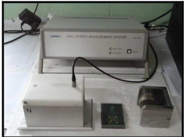
Chemical Bath Deposition is a convenient and low cost technique for producing large area thin film for semiconducting materials, used to deposit on the sub-strates. The deposition by chemical bath method is fre-quently carried out in an aqueous solution containing specific chemicals. In the CBD process, the precipita-tion of compound semiconductor is controlled through the use of suitable complexing agents and the amount of ions. However, CBD technology lacks mainly in as-pects such as chemical kinetics and growth mecha-nisms, which have significant relevance to improving the quality of the materials and processes. A simple chemical bath deposition (CBD) set-up was fabricated in the present work for large area deposition of thin films. This is an inexpensive technique at low deposi-tion temperatures. In addideposi-tion, the process can be con-trolled simply by varying pH, time, temperature, and concentration. Thin films of copper selenide (CuSe), cadmium selenide (CdSe), zinc selenide (ZnSe), lead sulphide (PbS), zinc sulphide (ZnS), and cadmium sul-phide (CdS) were prepared by CBD method [6-9]. In this work ECOPIA Hall Effect measurement system was used to study the electrical properties such as re-sistivity, carrier concentration, Hall mobility, Hall coef-ficient and conductivity of the deposited thin films. The experimental set-up of Hall Effect is shown in Fig. 1.
3. HALL EFFECT MEASUREMENTS
S. THIRUMAVALAVANA,K.MANI,S. SURESH SAGADEVAN J.NANO-ELECTRON.PHYS. 7, 04024 (2015)
04024-2 current perpendicular to both the magnetic field and the current, which in turn creates a transverse voltage that is perpendicular to both the magnetic field and the current. The underlying principle is the Lorentz force, that is, the force on a point charge due to electromag-netic fields. Electrical properties such as resistivity, carrier concentration and Hall mobility were estimated from Hall measurements in Van Der Pauw configura-tion at room temperature.
Fig. 1– Hall Effect instrument experimental set-up
3.1 Van Der Pauw Configuration
The standard Van Der Pauw technique is employed to determine the Hall parameters. From the Hall pa-rameters, one can determine the type of the charge carriers, carrier concentration, mobility of the charge carriers, and Hall coefficient of the films. The Van Der Pauw method involves applying a current and measur-ing the voltage usmeasur-ing four small contacts on the circum-ference of a flat, arbitrarily shaped sample of uniform thickness. This method is particularly useful for meas-uring very small samples because geometric spacing of the contacts is unimportant. Effect due to the size of a sample, which is the approximate probe spacing, is irrelevant. Using this method, the resistivity can be derived from a total of eight measurements that are made around the periphery of the sample with the con-figurations shown in Fig. 2.
The voltage measurements were taken; two values of resistivity, A and B were derived using the relations
1 2 3 4
2 4
A A s
V V V V
f t
In I
(1)
Fig. 2 –Symmetric contacts in Van Der Pauw configuration
5 6 7 8
2 4
B B s
V V V V
f t
In I
(2)
where, A and B are resistivities in Ω-cm, ts is the
sample thickness in m, V1-V8 represents the voltages measured by the voltmeter, I is the current passing through the sample in amperes, fA and fB are
geomet-rical factors based on sample symmetry. Once A and
B are known, the average resistivity (AVG) can be
de-termined as follows:
2
A B
AVG
(3)
The Hall signal was measured between two ends while the current was passing through the other two ends. Hall mobility () is given by the ratio
8 10
sh
R BR
(4)
where ΔR is the change in resistance due to the mag-netic field (B) which is applied to measure Hall voltag-es and Rsh is sheet resistance of the material. The
re-sistivity () is proportional to the reciprocal of the product of the free carrier concentration (n) and the mobility () as is shown in the following relation
1 en
(5)
The Hall coefficient RH is given by,
H
R (6)
The type of carriers can be understood from the sign of the RH and thus the type of conductivity can be identified. The negative value of RH corresponds to the flow of electrons (n-type) and positive value corre-sponds to the flow of holes (p-type) [10].
4. DC CONDUCTIVITY STUDY
The DC conductivity of the thin films was measured using the two-probe technique. The samples were par-allel to the cleavage plane to the desired thickness of 1-2 mm. The opposite faces of the thin films were coated with good quality graphite to obtain a good ohmic con-tact with the electrodes. The resistance of the films was measured using a megohmmeter. The DC conductivity (σdc) of the film was calculated using the relation,
/ dc t RA
, (7)
where R is the measured resistance, t is the thickness of the sample, and A is the area of the face in contact with the electrode. The above procedure was used to determine the DC electrical conductivity. The general relation for the temperature variation of conductivity is given by
0exp /
dc E kT
, (8)
STUDIES ON HALL EFFECT AND DCCONDUCTIVITY MEASUREMENTS… J.NANO-ELECTRON.PHYS.7, 04024 (2015)
04024-3 is the Boltzmann’s constant. The above equation can be rewritten as
0
lndc ln E kT/ (9)
From the plot of lnσdc versus 1000 / T we get the slope (–E/k) and the intercept (lndc). It is customary
to plot lndc versus 1000 / T, from the slope of which
the activation energy (E) can be calculated.
5. RESULTS AND DISCUSSION
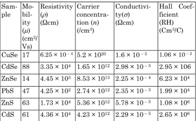
Hall Effect study is a powerful tool for knowing the electronic properties of Semiconductor. Hall measure-ments are done by Van Der Pauw method at room tem-perature The Hall effect can be described by means of the Hall Coefficient RH. The shape of the films is square with point ohmic electrodes being set at the four corners. Thin film samples of area one square cm pre-pared by (CBD) method were used to carry out the Hall studies. The gold spring probes were placed at the cor-ners of the sample symmetrically as shown in Fig. 2. A constant current of 1μA and 1nA was supplied to the films. The films were subjected to uniform magnetic field of 0.57 Tesla. A known current was passed through the electrodes of the films and voltage across the other two electrodes was measured. The polarity was reversed for each measurement and the voltage was measured. The electrical properties of the deposit-ed thin films were studideposit-ed with the help of Hall meas-urements in Van Der Pauw configuration (ECOPIA HMS-3000) at room temperature. Hall Effect parame-ters such as carrier mobility, carrier concentration (n), Hall coefficient (RH), resistivity, and the conductivity were calculated and presented in Table 1.
Table 1– Hall effect parameters for prepared thin films
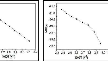
Electrical conductivity depends on the thermal treat-ment of thin films. The activation energy (Ea) was
cal-culated from the slope of the graph between lnσdc and 1000 / T (Figs. 1, 2, 3, 4 and 5). It was found to be 0.040 eV, 0.35 eV, 0.25 eV, 0.40 eV, and 0.60 eV for the thin films CuSe, CdSe, ZnSe, PbS, and ZnS respective-ly. Evaluation of DC electrical conductivity revealed useful information about materials that could be ex-ploited for various applications. The study of DC elec-trical conductivity sheds light on the behaviour of charge carriers under a DC field, their mobility and mechanism of conduction.
Fig. 1 –Plot of ln(dc) versus 1000 / T for CuSe films
Fig. 2– Plot of ln(dc) versus 1000 / T for CdSe films
Fig. 3 –Plot of ln(dc) versus 1000 / T for ZnSe films
6. CONCLUSION
Hall Effect measurements are used in many phases of the electronics industry, from basic materials research and device development to device manufacturing. Hall Effect parameters such as carrier mobility (), carrier concentration (n), Hall coefficient (RH), resistivity (),
Sam-ple Mo- bil-ity () (cm2/ Vs)
Resistivity ()
(Ωcm)
Carrier concentra-tion (n) (/cm3)
Conductivi-ty()
(Ωcm)
Hall Coef-ficient (RH) (Cm3/C)
CuSe 17 6.25 × 10– 4 5.2 × 10²⁰ 1.6 × 10– 5 1.06 × 10– 2
CdSe 88 3.35 × 10⁴ 1.65 × 10¹² 2.98 × 10– 5 2.95 × 10⁶
ZnSe 14 4.45 × 10³ 8.53 × 10¹³ 2.25 × 10– 4 6.23 × 10⁴
PbS 47 4.25 × 10² 2.74 × 10¹² 2.35 × 10– 3 1.99 × 10⁴
ZnS 63 1.73 × 10⁴ 5.36 × 10¹² 5.78 × 10– 5 1.08 × 10⁶
S. THIRUMAVALAVANA,K.MANI,S. SURESH SAGADEVAN J.NANO-ELECTRON.PHYS. 7, 04024 (2015)
04024-4
Fig. 4 –Plot of ln(dc) versus 1000 / T for PbS films Fig. 5 –Plot of ln(dc) versus 1000 / T for ZnS films
and the conductivity () were calculated on CuSe, CdSe, ZnSe, PbS, ZnS, and CdS thin films. Thus, the electrical properties of the semiconductor thin films were obtained by the Van Der Pauw method. The
acti-vation energy was calculated from DC conductivity studies. It was found to be 0.040 eV, 0.35 eV, 0.25 eV, 0.40 eV, and 0.60 eV for the thin films CuSe, CdSe, ZnSe, PbS, and ZnS respectively.
REFERENCES
1. L.J. Van der Pauw, Philips Res. Report.13, 1 (1958). 2. D.W. Koon, C.J. Knickerbocker, Rev. Sci. Instrum. 67,
4282 (1996).
3. D.W. Koon, Rev. Sci. Instrum.77, 094703 (2006).
4. O. Bierwagen, T. Ive, C.G. Van de Walle, J.S. Speck, Appl. Phys. Lett.93, 242108 (2008).
5. N. Yom-Tov, C. Saguy, A. Bolker, R. Kalish, Y.E. Yaish,
J. Appl. Phys.108, 043711 (2010).
6. S. Thirumavalavan, K. Mani, Suresh Sagadevan, Chalco-genide Lett.12, 237 (2015).
7. S. Thirumavalavan, K. Mani, S. Sagadevan, J. Ovonic Res.
11, 203 (2015).
8. S. Thirumavalavan, K. Mani, Suresh Sagadevan, Int. J. Phys. Sci.10 No 6, 204 (2015).
9. S. Thirumavalavan, K. Mani, S. Sagadevan, Sci. Res. Es-says10, 378 (2015).