Optical and Electrical Properties of Chemical Bath Deposited Cobalt Sulphide Thin Films
Geetha Govindasamya, Priya Murugasenb*, Suresh Sagadevanc
Received: June 10, 2016; Revised: August 14, 2016; Accepted: September 7, 2016
Cobalt sulphide (CoS) thin ilms were synthesized using the Chemical Bath Deposition (CBD) technique. X-ray difraction (XRD) analysis was used to study the structure and the crystallite size of CoS thin ilm. Scanning Electron Microscope (SEM) studies reveal the surface morphology of these ilms. The optical properties of the CoS thin ilms were determined using UV-Visible absorption spectrum. The optical band gap of the thin ilms was found to be 1.6 eV. Optical constants such as the refractive index, the extinction coeicient and the electric susceptibility were determined. The dielectric studies were carried out at diferent frequencies and at diferent temperatures for the prepared CoS thin ilms. In addition, the plasma energy of the valence electron, Penn gap or average energy gap, the Fermi energy and electronic polarizability of the thin ilms were determined. The AC electrical conductivity measurement was also carried out for the thin ilms. The activation energy was determined by using DC electrical conductivity measurement.
Keywords: CoS, CBD, XRD, SEM, Dielectric studies, AC and DC electrical conductivity measurement
* e-mail: [email protected]
1. Introduction
Thin ilms of metal chalcogenide have been studied extensively in recent years due to their applications in
photovoltaic and opto-electronic devices1. Thin ilms are
thin material layers ranging from fractions of a nanometer
to several micrometers in thickness. Cobalt sulphide (CoS)
has wide range of applications in solar selective coatings, IR
detectors and as a storage electrode in photoelectrochemical
storage device. Growth of the metal chalcogenide thin ilms via chemical solution deposition or chemical bath deposition or chemical growth process route is one of the key technologies today2-4. The CoS thin ilms can be
prepared using chemical bath deposition (CDB) method5,6.
Recently, synthesis of CoS thin ilms was carried out by a modiied liquid phase chemical growth process7,8. In chemical methods, the deposition parameters such as pH, temperature,
concentration of the solution and deposition time inluence the formation of nanocrystalline thin ilms and crystallite size, which in turn engineer the bandgap of the material. Chemical bath deposition technique (CBD) is one of the most promising methods for making large area high quality nanocrystalline thin ilms for photovoltaic applications because it is an eicient and cost efective method. In this study, chemical bath deposition technique was employed to deposit the thin ilm of cobalt sulphide on microscopic glass. The prepared ilms were characterized for their structural, surface morphology, optical, and electrical properties.
2. Experimental Procedure
Chemical bath deposition technique was used for the deposition of CoS thin ilms. The substrates were washed using soap solution and subsequently kept in hot chromic acid and then ultrasonically cleaned with deionized water for 10 min and wiped with acetone and stored in a hot oven. The growth solution consisted of 10 ml of Cobalt (II) sulfate, 2 ml triethanolamine, 15 ml ammonia, 10 ml of thiourea and double distilled water, which were mixed thoroughly. The deposition was carried out at a temperature of 110°C. A glass substrate was placed vertically inside the vessel with the help of a suitably designed substrate holder. After a time period of 60 min, the glass slide was removed from the bath and cleaned with deionized water and dried in the hot oven. Many trials were made by optimizing the deposition parameters to obtain a good quality CoS thin ilm. The resultant ilms were found to be homogeneous and well adhered to the substrate with mirror like surface. The XRD pattern of the CoS thin ilms was recorded by using powder X-ray difractometer (Schimadzu model: XRD 6000 and CuKα (λ=0.154 nm)) with difraction angle between 20° and 70°. The crystallite size was determined using the Debye Scherrer’s formula for the broadenings of the corresponding X-ray spectral peaks. A VARIAN CARY MODEL 5000 spectrophotometer was used for recording the optical absorption spectrum in the wavelength range of 400 – 800 nm. The dielectric properties of the CoS thin ilms were analyzed using a HIOKI 3532-50 LCR HITESTER for a frequency range from 50Hz-5MHz.
a R&D Centre, Bharathiar University, Coimbatore, India
3. Results and Discussion
3.1. Structural characterization
The XRD pattern of the CoS thin ilms was recorded by using a powder X-ray difractometer, with a difraction angle between 20° and 70° and is shown in Figure 1. The pattern revealed hexagonal wurtzite polycrystalline structure of CoS ilms. The well deined peaks were observed in the
pattern. The excellent peaks (100), (101), (102), (110),
(103), (200), and (112) were obtained in the powder X-ray difraction studies. No impurity peaks were observed in the XRD patterns. The average crystalline size (D) was calculated using the Debye-Scherrer formula,
.
( )
cos
D
=
b
0 9
m
i
1
where λ is the X-ray wavelength, θ is the Bragg difraction angle, and β is the FWHM of the XRD peak appearing at the difraction angle θ. The average crystalline size was calculated from X-ray line broadening peak and Debye-Scherrer equation and it was found to be about 14 nm.
3.2. Surface Analysis
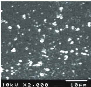
Scanning Electron Microscope (SEM) is very helpful to study the surface morphology of ilms. SEM images give information regarding the surface structure and roughness. SEM image obtained for CoS thin ilm deposited on glass substrate is shown in Figure 2. The CoS thin ilms exhibited more or less uniform surface morphology. The thickness of the obtained ilm is 2 mm and the mean crystallite size was found to be about12 nm.
3.3. UV-Visible spectroscopy
Optical investigations of the prepared ilms revealed that there was a band to band direct transition. The optical absorption spectrum of the CoS thin ilm was obtained in the wavelength range of 400 – 800 nm. Figure 3 shows the variation of the optical absorbance with the wavelength of the CoS thin ilms which shows the edge shift towards longer wavelength region (red shift). It is observed that the optical absorption decreases smoothly from UV to near IR region. This validates the material’s suitability in devices used for good absorption of UV radiation, that is to say, it can be used as a UV ilter9. The optical absorption coeicient (α) was
calculated from transmittance using the relation
coeicient (α) obeying the following relation for high photon energies (hν)
( )
log
d
T
1
1
2
a
=
S X
where T is the transmittance and d is the thickness of the ilms. The ilms under study have an absorption
( )
hv
A hv
E
3
/ g1 2
a
=
Q
-
V
where Eg is the optical band gap of the ilms and A is a
constant. The fundamental absorption corresponding to the optical transition of the electrons from the valence band to
the conduction band can be used to determine the nature
and value of the optical band gap Eg of the ilms. A plot of variation of (αhν)2 versus hν is shown in Figure 4. E
g could
be evaluated using the extrapolation of the linear part. The intercept on energy axis gives the value of band gap energy and it was found to be 1.6 eV. This bandgap narrowing indicates that the top of the valence band and the bottom of the conduction band are modiied with increasing substrate
temperature to various extents10,11.
3.3.1. Determination of Optical Constants
Two of the most important optical properties, viz., the refractive index (n) and the extinction coeicient (K) are generally called optical constants. The amount of light that transmits through thin ilm material depends on the amount of the relection and the absorption that take place along the light path. The optical constants such as the refractive index
(n), the real dielectric constant (er) and the imaginary part
of the dielectric constant (ei) were calculated.The extinction
coeicient (K) was obtained from the following equation
( )
K
=
ma
4
r
4
The extinction coeicient (K) was found to be 0.0044 at λ =800 nm. The transmittance (T) is given by
( )
exp
exp
T
R
t
R
t
1
2
1
5
22
a
a
=
Q
-
-
V
Q
-
Q
-
V
V
Relectance (R) in terms of absorption coeicient was obtained from the above equation.
Hence,
( )
exp
exp
exp
R
t
t
t
1
1
1
6
!
a
a
a
=
-
+
R
-
Q
-
+
V
Q
V
W
Refractive index (n) could be determined from the relectance data using the following equation
( )
n
R
R
R
R
2
1
1
3
10
3
7
2!
-The refractive index (n) was found to be 1.43 at λ =800 nm. From the optical constants, electric susceptibility (χc)
could be calculated from the following relation
( )
n
k
4
8
r 0 C 2 2
f
=
f
+
r|
=
-Hence, we have
( )
n
k
4
9
C
2 2 0
|
=
-
r
-
f
Where ε0 is the permittivity of free space. The value of
the electric susceptibility (χc) was 1.044 at λ=800 nm. Since
electrical susceptibility was greater than 1, the material could be easily polarized when the incident light was more intense. The real part of the dielectric constant (εr) and the imaginary
part of the dielectric constant (εi) could be calculated from
the following relations
( )
n
k
10
r
2 2
f
=
-( )
nk
2
11
i
f
=
The values of the real dielectric constant (εr) and the
imaginary dielectric constant (εi) at λ = 800 nm were
estimated to be 3.241 and 0.0041 respectively. The lower value of the dielectric constant made it possible to cause induced polarization due to intense incident light radiation.
3.4. Dielectric Studies
The electrical properties of the materials are of great importance in determining the usage of the film for photovoltaic applications. The electrical property depends on various growth parameters such as ilm composition, thickness, rate of deposition, and substrate temperature. The dielectric constant and the dielectric loss were calculated at
Figure 1: XRD spectrum of CoS thin ilms.
Figure 2: SEM Image of the CoS thin ilms
Figure 3: Optical absorption spectrum of CoS thin ilm
Figure 5: Dielectric constant of CoS thin ilm
diferent frequencies and temperatures and their variations with log f are shown in Figures 5 and 6. It is observed that the dielectric constant decreases with rising frequency and then achieves almost a constant value in the high frequency region. The net polarization of CoS thin ilm is owing to ionic, electronic, dipolar and space charge polarizations. The huge valued dielectric constant at low frequencies can be attributed to the lower electrostatic binding strength, arising due to the space charge polarization near the grain boundary interfaces12. Owing to the application of an electric
ield, the space charges are stimulated and dipole moments are produced and this is called space-charge polarization13.
Apart from this, these dipole moments are rotated by the ield applied ensuing in rotation polarization which also contributes to the high values. Figure 6 shows the dielectric loss as a function of frequency. These curves show that comparable to that of the dielectric constant, the dielectric loss depends on the frequency of the applied ield. The dielectric loss decreases with an increase in the frequency
at almost all temperatures, but appears to attain saturation
in the higher frequency range at all the temperatures14. The
amount of charge carriers increases by thermal activation and the place of loss peak shifts to top frequency with increasing temperature being indicated by the rise in the maximum out value of dielectric loss with temperature15.
The high frequency dielectric constant is required as
input, to evaluate electronic properties such as valence
electron plasma energy, average energy gap or Penn gap, Fermi energy and electronic polarizability of the CoS thin ilms. The theoretical calculations showed that the high frequency dielectric constant was explicitly dependent on the valence electron Plasma energy, an average energy gap referred to as the Penn gap and Fermi energy. The Penn gap is determined by itting the dielectric constant with the Plasmon energy.
Figure 6: Dielectric loss of CoS thin ilm
The following relation was used to calculate the valence electron plasma energy, ћωp
.
Z
M
( )
28 8
/12
P
1 2
&
~
=
T
t
Y
According to the Penn model, the average energy gap for the CoS thin ilms is given by
( )
E
p
1
/13
P 1 2
&
f
~
=
-3
Q
V
Where ωPis the valence electron plasmon energy and
the Fermi energy is given by
.
( )
E
F0 2948
P /14
4 3&
~
=
Q
V
Then, the electronic polarizability (α), is given by
.
( )
S
E
S
M
cm
3
0 396
10
15
P P
P 2
0 2
2 0
24 3
#
#
#
&
&
t
a
=
~
~
+
-Q
Q
V
V
#
&
Where S0 is a constant given by
( )
S
E
E
E
E
1
4
3
1
4
16
F P
F P 0
2
= -
#
&
+
#
&
The Clausius-Mossotti relation also gives α:
( )
N
M
4
3
2
1
17
a
=
r at f
f
+
-3 3
#
&
.
.
( )
E
M
cm
1 4 06
g0 396
10
24 318
#
#
#
a
= -
#
&
t
-where Eg is the bandgap value determined through the
UV-Visible spectrum. The high frequency dielectric constant of the materials is a very important parameter for calculating the physical or electronic properties of materials16. All the
above parameters as estimated from our experiments are shown in Table 1.
Table 1: Electronic parameters of the CoS thin ilms
Parameter Value
Plasma energy (hωp) 19.93 eV
Penn gap (Ep) 1.55 eV
Fermi Energy (EF) 15.77 eV
Electronic polarizability (using the Penn
analysis) 4.72 x 10
-24 cm3
Electronic polarizability (using the
Clausius-Mossotti relation) 4.84 x 10
-24 cm3
Electronic polarizability (using bandgap) 4.55 x 10⁻²⁴ cm3
( )
tan
19
ac 0 r
v
=
f f ~
d
( )
RA
t
20
dc
v
=
3.5. AC conductivity (
σ
ac)
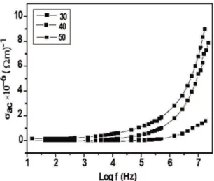
AC conductivity measurements were made in the frequency range 20 Hz to 1 MHz using HIOKI 3532-50 LCR HITESTER. A chromel-Alumel thermocouple was employed to record the sample temperature. A 30 minute interval was maintained prior to thermal stabilization after each measuring temperature. The ac conductivity (σac) was
calculated using the formula
Where εo is the vacuum dielectric constant (8.85 × 10
−12
farad/m), εr is the relative dielectric constant and ω is the angular
frequency ω=2πυ of the applied ield. Figure 7 shows the variation of ac conductivity with frequency and temperature. It is seen that the value of ac conductivity increases with increase in the frequency. There is a small increase in the electrical conductivity of the nanomaterial for an increase in frequency and is the same for all temperatures at the low frequency region. The increase in conductivity with temperature may be explained based on the assumption that within the bulk, the oxygen vacancies due to the loss of oxygen are usually created during increase in temperature and the charge compensation, which would leave behind free electrons at higher frequencies only. In metal
oxides, electrical conduction occurs through strong coupling
between phonons and electrons with the creation of polarons.
3.6. DC conductivity (σ
dc)
The dc conductivity measurements of CoS thin ilms were carried out. The dc conductivity σdcof the CoS thin ilms was calculated using the relation
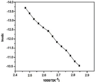
Where, R is the measured resistance, t is the thickness of the films and A is the area of the films in contact with the electrode. Figure 8 shows the variation of σdc
conductivity versus temperatures. It could be seen that the dc conductivity was increasing with increase in
temperature17. Traps which are present in the CoS thin
films may be filled by excitation at low temperature and may be emptied by raising the temperature by thermal activation. Upon thermal activation, the mobility of charge carriers increases with a possible mechanism of
hopping to cross the potential barrier and hence produce
enhanced current. The value of activation energy was determined from the slope of lnσdc versus 1000/ T (Figure
9) which was found to be 0.40 eV.
Figure 7: Variation of ac conductivity with frequency at various
temperatures.
Figure 9: Plot of lnσdc versus 1000/T (K -1)
4. Conclusions
The CoS thin ilm was synthesized by CBD technique. The XRD studies revealed that the CoS thin ilm was in hexagonal phase and the crystallite size was found to be 14 nm. The morphology of the CoS thin ilms was characterized by using SEM. The optical band gap was found to be 1.6 eV. The optical constants such as the refractive index, the extinction coeicient and the electrical susceptibility were calculated. The dielectric properties of the CoS thin ilms were calculated at diferent frequencies and temperatures. In addition, the plasma energy of the valence electron, Penn gap or average energy gap, the Fermi energy, and electronic polarizability of CoS thin ilms were also determined. The AC electrical conductivity was found to increase with an increase in the temperature and frequency. The DC conductivity study also revealed that the DC conductivity increased with increase in temperature. The activation energy was found to be 0.40eV. The obtained values for electrical conductivity and
optical constants made the material to be a good candidate
for photovoltaic and opto-electronic applications.
5. References
1. Cruz-Vázquez C, Inoue M, Inoue MB, Bernal R, Espinza Beltrán
FJ. Electrical and spectroscopic properties of amorphous copper sulide ilms treated with iodine, lithium iodide and sodium
iodide. Thin Solid Films. 2000;373(1):1-5.
2. Karande VS, Mane SH, Pujari VB, Deshmukh LP. (Cd, Mn) Se semimagnetic semiconductor thin ilms: growth from solution,
structural analysis and optical properties. Materials Letters.
2005;59(2-3):148-152.
3. Karande VS, Mane SH, Pujari VB, Deshmukh LP, Wadgaonkar
AR. Electrochemical studies of n-Cd1−xMnxSe thin film
photodetector. Journal of Materials Science: Materials in Electronics. 2004;15(7):419-423.
4. Hodes G. Semiconductor and ceramic nanoparticle ilms deposited by chemical bath deposition. Phys. Chem. Chem. Phys. 2007;9(18):2181-2196.
5. Basu PK, Pramanik P. Solution growth technique for the deposition
of cobalt sulphide thin ilm. Journal of Materials Science
Letters. 1986;5(12):1216-1218.
6. Eze FC, Okeke CE.Chemical-bath-deposited cobalt sulphide ilms: preparation efects Chemical-bath-deposited cobalt
sulphide ilms: preparation efects.Materials Chemistry and
Physics. 1997;47(1):31-36.
7. Mane ST, Kamble SS, Deshmukh LP. Cobalt sulphide thin ilms:
Chemical bath deposition, growth and properties. Materials
Letters. 2011;65(17-18):2639-2641.
8. Yu Z, Du J, Guo S, Zhang J, Matsumoto Y. CoS thin ilms
prepared with modiied chemical bath deposition. Thin Solid
Films. 2002;415(1-2):173-176.
9. Okoli DN, Okoli C. Optimal Growth and Characterization of Cobalt Sulphide Thin Films Fabricated Using the Chemical
Bath Deposition Technique. Journal of Natural Sciences
Research. 2012;2(3):5-8.
10. Zhou J, Bian GQ, Zhu QY, Zhang Y, Li CY, Dai J. Solvothermal
crystal growth of CuSbQ2 (Q=S, Se) and the correlation between
macroscopic morphology and microscopic structure. Journal
of Solid State Chemistry. 2009;182(2):259-264.
11. Kassim A, Ho SM, Abdullah AH, Nagalingam S. XRD, AFM and UV-Vis Optical Studies of PbSe Thin Films Produced by
Chemical Bath Deposition Method. Transactions C: Chemistry
and Chemical Engineering. 2010;17(2):139-143.
12. Suresh S, Arunseshan C. Dielectric Properties of Cadmium Selenide (CdSe) Nanoparticles synthesized by solvothermal
method. Applied Nanoscience. 2014;4(2):179-184.
13. Suresh S.Studies on the dielectric properties of CdS nanoparticles.
Applied Nanoscience. 2014;4(3):325-329.
14. Sagadevan S, Sundaram AS. Dielectric properties of lead
sulphide thin ilms for solar cell applications. Chalcogenide
Letters. 2014;11(3):159-165.
15. Suresh S. Synthesis, structural and dielectric properties of zinc
sulide nanoparticles. International Journal of Physical Science.
2013;8(21):1121-1127.
16. Sagadevan S, Podder J. Optical and Electrical Properties of
Nanocrystalline SnO2 Thin Films Synthesized by Chemical Bath
Deposition Method. Soft Nanoscience Letters. 2015;5(4):55-64.
17. Thirumavalavan S, Mani K, Suresh S. Investigation on structural, optical, morphological and electrical properties of
lead sulphide (PbS) thin ilms. Journal of Ovonic Research.