A Differential Double Pass Transistor Logic Unit
Chiraz Khedhiri1, Mouna Karmani1 & Belgacem Hamdi1, 2 1
Electronic & Microelectronics Laboratory. Monastir – Tunisia
2
ISSAT, Sousse – Tunisia
Abstract
In this paper we present a new differential logic unit with duplicated functional outputs. The logic functions as well as their inverses are implemented within a single Logic Unit (LU) cell. The hardware overhead for the implementation of the proposed LU is lower than the hardware overhead required for standard LU implemented with standard CMOS logic style. This new implementation is attractive as fewer transistors are required to implement important logic functions. The proposed differential logic unit can perform 8 Boolean logical operations by using only 16 transistors.
Spice simulations using a 32nm technology was utilized to evaluate the performance of the proposed circuit.
Keywords: differential logic unit, double pass transistor logic, CMOS technology.
1. Introduction
Conventional static CMOS has been a technique of choice in most processor design [1]. Alternatively, static pass transistor circuits have also been suggested for low-power applications [2].
Indeed, designing high-speed low-power circuits with CMOS technology has been a major research problem for many years. Several logic families have been proposed and used to improve circuit performance beyond that of conventional static CMOS family.
In addition, due to technology scaling and the increasing number of transistors on chip, the performance of static CMOS circuits comes at substantial area/power dissipation costs that may be critical, especially for portable appliances. New logic families that address the power and performance challenges must be therefore, explored [3].
The Pass-Transistor Logic (PTL) is a better way to implement circuits designed for low power applications. The advantage is that one pass-transistor network (either PMOS or NMOS) is sufficient to implement the logic function, which results in smaller number of transistors and smaller input load.
There are two main pass-transistor circuit styles: those that use NMOS only pass-transistor circuits, like CPL [4], and those that use both NMOS and PMOS pass-transistors, like DPL [5] and DVL [6].
Recently, several researchers have attempted to use Complementary pass transistor logic (CPL) to realize static and high performance designs in different digital systems [4–7].
However, since only NMOS transistors are used in CPL gates, the voltage swing at the end of a pass transistor network has a swing from 0 to VDD - VTH; therefore PMOS
transistors at the following static gates are not completely off resulting in static power dissipation.
This problem is usually solved by a PMOS level restorer transistor to pull up the node to VDD. The level restorer
adds hysteresis to the gate and degrades the performance. Also, the delay of pass transistor networks increases quadratically with the number of stages and as a result, some intermediate buffers should be used to make strong VDD and ground. All these problems arise from the fact
that NMOS transistors can not pass VDDfaithfully to the
other side. The solution is using a complementary PMOS transistor in parallel with NMOS to generate a strong VDD
at the output [8]. This structure is double pass transistor logic (DPL).
DPL uses both PMOS and NMOS devices in the pass-transistor network to avoid non full swing problems [9]. Double pass-transistor logic is shown to improve circuit performance at reduced supply voltage. Its symmetrical arrangement and double-transmission characteristics improve the gate speed without increasing the input capacitance [5].
In this paper, we propose a differential logic unit implemented in CMOS double pass transistor logic. The proposed logic unit (LU) is low power and small number of transistors design. It performs 8 logic functions with only 16 transistors.
IJCSI International Journal of Computer Science Issues, Vol. 9, Issue 2, No 1, March 2012 ISSN (Online): 1694-0814
www.IJCSI.org 351
The paper is organized as follows. Section II describes the proposed design. In section III, we present the simulation results. Conclusions are given in section VI.
2. Proposed Design
ALU stands for the Arithmetic logic unit and it is an internal part of the processor which is used for all the mathematical and logical operations. The operations of the ALU include arithmetic operations such as addition, subtraction, multiplication and division of the binary values. It also, performs some logical operations such as AND, OR and XOR, integer arithmetic operations and Bit-shifting operations etc. ALU is the fundamental building block of the processor.
Today, modern computers contain very complex ALU for performing the complex calculations and logical operations inside the computer. The data or the operands are the input of the ALU and it generates the output as the result of the computation.
In some of the computers the ALU is divided into two units: Arithmetic unit and Logic unit.
Logic units are the building blocks of many important computational operations likes arithmetic, multiplexer-demultiplexer, parity checker, sum generator, etc... Multifunctional logic operation is very much essential in this respect.
In this paper, a differential logic unit is proposed that can perform 8 Boolean logical operations by using only 16 transistors. The circuit is implemented using the double pass transistor logic (DPL).
The bit slice of the proposed differential logic unit performing XOR, XNOR OR, NOR, AND, NAND, VDD and VSS is given in Fig. 1. It performs: XOR/XNOR for (SO,S1) = (0, 0) , OR/NOR for (SO,S1) = (0, 1) , NAND/AND for (SO,S1) = (1, 0) and VDD/VSS for (SO,S1) = (1, 1).
B
A A
B
O ut O ut
B
A A
B
A
S0
S 1
Fig. 1. The proposed differential logic unit
Fig. 1 shows a differential logic unit which consists of double pass transistors and inverter gates. Inputs A, S0 and S1 control the “ON” and “OFF” switching of the pass transistors.
Such obtained logic is differential as every variable is represented in its true and complement form.
Output inverters are added to ensure the drivability and outputs restoration.
The functions performed by the circuit of Fig. 1 are resumed in table I.
Table 1 : The Logic Unit truth table
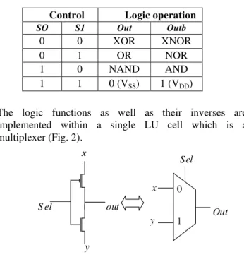
The logic functions as well as their inverses are implemented within a single LU cell which is a multiplexer (Fig. 2).
S el out
x
y
x
y
Sel
Out
0
1
Fig. 2. The basic logic unit cell
Control Logic operation
SO S1 Out Outb
0 0 XOR XNOR
0 1 OR NOR
1 0 NAND AND
1 1 0 (VSS) 1 (VDD)
IJCSI International Journal of Computer Science Issues, Vol. 9, Issue 2, No 1, March 2012 ISSN (Online): 1694-0814
www.IJCSI.org 352
A circuit that generates an output that exactly reflects state of one of a number of data inputs, based on value of one or more control inputs is called “multiplexer” [10].
Multiplexer is an important part in implementation of signal control systems and memory circuits, since it allows us to choose one of the inputs and transfer it to the output. The functionality of multiplexer is shown in (1). x and y are the two inputs and Sel is used to select one between the two inputs [11].
.
.
Out
x Sel
y Sel
(1)The proposed logic unit is implemented using the double pass transistor logic. This structure uses only 16 transistors.
3. Simulation Results
Before implementing the whole circuit, a gate-level schematic in DSCH3 is generated. DSCH3 program is a logic editor and simulator used to validate the architecture of logical circuit, before microelectronics started. It provides user friendly environment for hierarchical logic design and fast simulation with delay analysis, which allows design and validation of complex logic structures.
After successful simulation we implemented the above designs of the logic unit with different components using Microwind 3.1 layout tool [12] for its ease of use and availability.
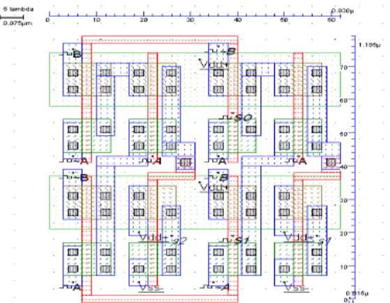
The differential logic unit of the Fig. 1 is implemented in full-custom 32nm CMOS technology at 0.8V power supply [12]. SPICE simulations of the circuit extracted from the layout, including parasitic, are used to demonstrate that this circuit has an acceptable electrical behavior. The layout of the differential logic unit with the two restoring inverters is as shown in Fig.3. It occupies an area of 0.93×1.185µm2.
Fig. 3. Layout of the logic unit in CMOS 32nm Double Pass Transistor Logic
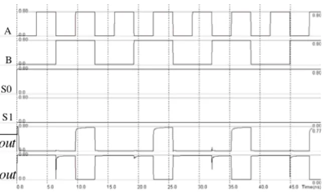
Fig. 4, 5, 6 and 7 illustrates a SPICE simulation of the circuit of Fig. 3.
A
B
S0
S1
out
out
Fig. 4. The dual rail XOR/XNOR function for (S0, S1) = (0,0)
The above simulation show that when (SO,S1) = (0,0), out
= XOR and out = XNOR.
A
B
S0
S1
out
out
Fig. 5. The dual rail OR/NOR function for (S0, S1) = (0,1)
When (SO,S1) = (0,1), out = OR and out = NOR.
IJCSI International Journal of Computer Science Issues, Vol. 9, Issue 2, No 1, March 2012 ISSN (Online): 1694-0814
www.IJCSI.org 353
A
B
S0
S1
out
out
Fig. 6. The dual rail AND/NAND function for (S0, S1) = (1,0)
When (SO,S1) = (1,0), out = NAND and out = AND
A
B
S0
S1
out
out
Fig. 7. The VDD/VSS function for (S0,S1) = (1,1)
For (SO,S1) = (1,1), out = VDD and out = VSS
Controlled by the two function select inputs (S0 and S1), the logic unit can perform 8 possible logic operations using only 16 transistors.
The circuit is implemented with double pass transistor CMOS technology. Pass transistor logic is attractive as fewer transistors are needed to implement important logic functions, smaller transistors and smaller capacitances are required, and it is faster than conventional CMOS. However, the pass transistor gates generate degraded signals, which slow down signal propagation [13]. This degradation is corrected by inserting two inverters at the outputs of the circuit.
4. Conclusion
Logic units are the building blocks of many important computational operations likes arithmetic, multiplexer-demultiplexer, parity checker, sum generator, etc...
In this paper, a new differential CMOS logic unit circuit based on double pass transistors is proposed. This implementation is low power, low cost design with only 16 transistors to perform 8 logic functions. In order to
evaluate the usefulness of the proposed scheme, one bit Logic Unit was implemented and simulated. The proposed Logic Unit can operate at low voltages, yet giving quite a good speed.
References
[1] Jan M Rabaey, Anantha Chandrakasan, Borivoje Nikolic, "Digital Integrated Circuits: A Design perspective", 2nd Edition, Prentice-Hall, Inc.
[2] K.Yano, Y.Sasaki, K.Rikino, K.Seki, "TOP-DOWN PASS- TRANSISTER LOGIC DESIGN", IEEE Journal of Solid- state Circuits, Vol.31, pp.792-803.1996.
[3] Rupesh S. Shelar and Sachin S. Sapatnekar, "BDD Decomposition for Delay Oriented Pass Transistor Logic Synthesis", IEEE TRANSACTIONS ON VLSI SYSTEMS, Vol. 13, 2005, pp. 957-970.
[4] K. Yano, T. Yamanaka, T. Nishida, M. Sato, K. Shimohigashi, and A. Shimizu, "A 3.8 ns CMOS 16 * 16 multiplier using complementary pass-gate transistor logic", IEEE J. Solid-Sate Circuits, vol. 25, 1990, pp. 388–395. [5] M. Suzuki et al., "A 1.5 ns 32-bit CMOS ALU in double pass-transistor logic", in Proc. IEEE Int. Solid-State Circuits Conf., Feb. 1993, vol. 36, pp. 90–91.
[6] V.G. Oklobdzˇija, B. Duchene, "Pass-Transistor Dual Value Logic for Low-Power CMOS", Proceedings of the 1995 International Symposium on VLSI Technology, Systems, and Applications, May–June, 1995, pp. 341–344.
[7] Parameswar, H. Hara, and T. Sakurai, "A high speed, low power, swing restored pass-transistor logic based multiply and accumulate circuit for multimedia application", in Proc. IEEE CICC, 1994, pp. 278–281
[8] Shahrzad Naraghi, "Reduced Swing Domino Techniques for Low Power and High Performance Arithmetic Circuits", thesis, Electrical and Computer Engineering, Waterloo, Ontario, Canada, 2004.
[9] Akilesh Parameswar, Hiroyuki Hara and Takayasu Sakurai, "A Swing Restored Pass-Transistor Logic-Based Multiply and Accumulate Circuit for Multimedia Applications", IEEE JOURNAL OF SOLID-STATE CIRCUITS, Vol. 31, No. 6, June 1996, pp. 804-809.
[10] G.L.Madhumati, M.Madhavilatha, and K.Ramakoteswara Rao, "Power and Delay Analysis of a 2-to-1 Multiplexer Implemented in Multiple Logic Styles for Multiplexer- Based Decoder in Flash ADC", International Journal of Recent Trends in Engineering, Vol. 1, No. 4, May 2009, pp. 29-31.
[11] Arman Roohi, Hossein Khademolhosseini, Samira Sayedsalehi, Keivan Navi, "A Novel Architecture for Quantum-Dot Cellular Automata Multiplexer", IJCSI International Journal of Computer Science Issues, Vol. 8, Issue 6, No 1, November 2011, pp.55-60.
[12] E. Sicard, "Microwind and Dsch version 3.1", Toulouse: INSA, ISBN 2-87649-050-1, December 2006.
[13] B. Hamdi, C. Khedhiri, and R. Tourki, "Pass Transistor Based Self-Checking Full Adder", International Journal of Computer Theory and Engineering, Vol. 3, No. 5, October 2011, pp.608-616.
IJCSI International Journal of Computer Science Issues, Vol. 9, Issue 2, No 1, March 2012 ISSN (Online): 1694-0814
www.IJCSI.org 354