Chennai, India
[email protected], 8870283746
Abstract: Adders are the most important arithmetic units in a general microprocessor and the major source of power dissipation. Apart from addition, adders are also used in performing useful operations such as subtraction, multiplication, division and address calculation etc. In this paper, we have presented the study of different logic style using 1-bit full adder circuit and we have compared this 1-bit full adder on certain parameters such as power, number of transistor and frequency using microwind and T-spice.
Keywords: full adder, PTL (Pass transistor logic), DPL (Double pass transistor logic), SR-CPL (Swing restored-complementary pass transistor logic), adiabatic logic, PFAL (Positive feedback adiabatic logic), low-power.
1. INTRODUCTION
Power minimization is one of the primary concerns in today VLSI design methodologies. In portable devices, it is important to prolong the battery life is as much as possible. We need low power operating circuits, in non-conventional power operating circuits like satellite, sensor application etc. Adder is the core component of an arithmetic unit. The eficiency of the adder determines the eficiency of the arithmetic unit. Addition is one of the important and commonly used arithmetic operation in many VLSI systems such application speciic DSP architectures, microprocessors and other applications.
In this paper we report the design of full adder based on DPL (Double pass transistor logic), SR-CPL (Swing restored-complementary pass transistor logic) and PFAL (Positive feedback adiabatic logic). Here the full adder implemented using alternative internal logic structure.
This paper is organized as follows section 2 presents previous works for designing a full-adder cell. Section 3 introduces the alternative internal logic structure to build the proposed full adders. Section 4 explains full adder implementation. Section 5 reviews the results obtained from the simulations. Section 6 concludes this work.
2. PREVIOUS WORK
Various low-power full adder circuits were developed using different logic styles such as standard CMOS [1], differential cascade voltage switch (DCVS), hybrid styles[3]-[5], and logic structure used to build the adder module[6],[7].
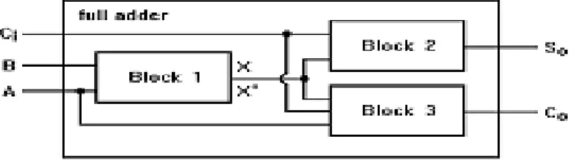
A full adder was presented in [8], which consists of three blocks XOR-XNOR gate to obtain A xor B and A xnor B blocks or multiplexers to obtain the sum(So) and carry(Co) outputs(Blocks 2 and 3).
The block 1 was effectively implemented in [9]. It consist of problem regarding propagation delay for a adder with logic structure shown in Fig.1,where the intermediate signal A xor B and its complement are then used to drive other blocks to generate inal outputs.
3. ALTERNATIVE INTERNAL LOGIC STRUCTURE FOR A FULL ADDER
Figure 1. Full Adder Cell formed by three main logic blocks
Figure 2. Alternative Internal Logic Structure for Full Adder
Table 1. Truth Table for Full Adder
A B C So Co
0 0 0 0 0
0 0 1 1 0
0 1 0 1 0
0 1 1 0 1
1 0 0 1 0
1 0 1 0 1
1 1 0 0 1
1 1 1 1 1
Thus, a multiplexer can be used to obtain the respective value taking the C input as the selection signal. Hence, an alternative logic structure to design a full adder circuit can be formed by a block to obtain the A xor B and A xnor B signals, another block to obtain the A.B and A+B signal, and two multiplexers being driven by the C input to generate the So and Co outputs, as shown in Fig.2 [9].
4. ADDER IMPLEMENTATION
In this we have designed a 1-bit full adder using DPL, SR-CPL and PFAL. The full adders are designed using 0.18µm CMOS technology.
4.1 FULL ADDER USING DPL LOGIC
Figure 5. Full Adder using DPL Logic
4.2 FULL ADDER USING SR-CPL LOGIC
Swing-restored CPL logic is derived from CPL logic. Output inverters are cross-coupled to a latch so that performs swing-restoration and output buffers at the same time. SR-CPL does not need any push-pull up PMOS networks.
Figure 6. Full Adder using SR-CPL Logic
The new logic structure presented in Fig.2.Fig.6 presents a full adder designed using SR-CPL logic to obtain xor/xnor gates, pass transistor based multiplexer to get So and Co and powerless and groundless pass transistor to get and/or gates. SR-CPL are used to implement complex gates with full output-swing.
4.3 FULL ADDER USING PFAL
Figure 7. PFAL Gate
Figure 8. Full Adder using PFAL (SUM)
PFAL 49 56 0.6 1.2
6. CONCLUSION
In this paper we analysed and compared the performance of full adder using different logic styles. The simulation results show that design based on adiabatic PFAL logic gives superior performance when compared to other logic styles even though their transistor count is high in some circuits. Depending on application, PFAL approach can be used to reduce the power and we can save energy upto 70% to 90%[10].
REFERENCES
[1] N.Weste and K.Eshraghain, Principles of CMOS VLSI design, system perspective. Reading, MA:Addison-Wesley,1988, ch.5.
[2] K.M.Chu and D.Pulfrey,A Comparison of CMOS circuit techniques: Differential cascade voltage switch logic versus conventional logic, IEEE J.Solid-state circuits, vol.SC-22, no.4, pp 528-532, AUG-1987.
[3] M.Zhang, J.Gu and C.H.Chang, A novel hybrid pass logic with static CMOS output drive full-adder cell, in proc, IEEE Int.Symp, Circuits Syst, May 2003, pp.317-320.
[4] C.Chang, J.Gu and M.Zhang, A review of 0.18µm full adder performances for tree structured arithmetic cir cuits, IEEE Trans, VLSI
Syst., vol.13, no.6, pp.686-695, jun.2005.
[5] S.Goel, A.Kumar and M.Bayoumi: Design of robust energy-eficient full adders for deep-submicrometer design using hybrid-CMOS
logic style, IEEE Trans, VLSI., vol.14, no.12, pp.1309-1320, Dec.2006.
[6] S.Agarwal, V.K.Pavankumar and R.Yokesh, Energy-eficient high performance circuits for arithmetic units, in Proc.2nd Int.Conf Emerging Trends Eng.Technol., Jul.2008, pp.371-376.
[7] D.Patel, P.G.Parate, P.S.Patil and S.Subbaraman, ASIC implementation of 1-bit full adder, in Proc.1st Int.Conf Emerging Trends Eng. Technol., Jul.2008, pp.463-467.
[8] N.Zhung and H.Wu, A new design of full adder, IEEE J.Solid state circuits, vol.27, no.5, pp.840-844, May-1992.
[9] M.Aguirre and M.Linares, An alternative logic approach to implement high-speed low power full adder cells, in Proc.SBCCI,
Flo-rianopolis, Brazil, Sep.2005, pp.166-177.
[10] A.Blotti and R.Saletti, Ultralow-Power Adiabatic Circuit Semi-Custom Design, IEEE Transcations on VLSI Systems, vol.12, no.11,