Design, Analysis, Implementation and Synthesis of 16 bit
Reversible ALU by using Xilinx 12.2
S.Anusha
1, M.Manoher Rao
2N.Swetha Reddy
31(Assistant Professor,Department of E.C.E, K.G.Reddy College of Engg &Tech, [email protected])
2(Assistant Professor,Department of E.C.E, K.G.Reddy College of Engg &Tech,[email protected]) 3
(P.G student ,Department of E.C.E, K.G.Reddy College of Engg &Tech,[email protected])
ABSTRACT
:
In the modern world, Arithmetic Logic Unit (ALU) is one of the most crucial components of any system and is used in many appliances like calculators, cell phones, and computers and so on. An arithmetic logic unit is a multi-functional circuit that conditionally performs one of several possible functions on two operands A and B depending on control inputs.
This paper proposes the design of programmable reversible logic gate structures, targeted for the ALU implementation and their use in the realization of an efficient reversible ALU. Reversible or information-lossless circuits have applications in digital signal processing, communication, computer graphics and cryptography. This ALU consists of thirteen operations, 5 arithmetic, 4 logical operations and 4 shifting operations. All the modules are being designed using the basic reversible gates. Using reversible logic gates instead of traditional logic AND/OR gates, a reversible ALU whose function is the same as traditional ALU is constructed. Comparing with the number of input bits and the discarded bits of the traditional ALU, the reversible ALU significantly reduce the use and loss of information bits. The proposed reversible 16-bit ALU reduces the information bits use and loss by reusing the logic information bits logically and realizes the goal of lowering power consumption of logic circuits. Programmable reversible logic gates are realized in Verilog by using XILINX 12.2.
Keywords –ALU,Digital Signal processing,power Consumption,Reversible logic gates.
I.INTRODUCTION
In modern VLSI system power dissipation is very high due to rapid switching of internal signals. The complexity of VLSI circuits increases with each year due to packing more and more logic elements into smaller volumes. Hence power dissipation has become the main area of concern in VLSI design. Reversible logic has its basics from thermodynamics of information processing. According to this, traditional irreversible circuits generate heat due to the loss of information during computation. In order to avoid this information loss the conventional circuits are modeled using reversible logic.
Landauer [1961] showed that the circuits designed using irreversible elements dissipate heat due to the loss of information bits. It is proved that the loss of one bit of information results in dissipation of KT*log2 joules of heat energy where K is the Boltzmann constant and T is the temperature at which the operation is performed. Benett [1973] showed that this heat dissipation due to information loss can be avoided if the circuit is designed using reversible logic gates.
A gate is considered to be reversible only if for each and every input there is a unique output assignment. Hence there is a one to one mapping between the input and output vectors. A reversible logic gate is an n input, n output device indicating that it has same number of inputs and outputs. A circuit that is built from reversible gates is known as reversible logic circuit[3].
II. Design of ALU
The design of low power and high speed microprocessors requires that its components should consume less power. Arithmetic and Logic Unit (ALU) is one of the most power consuming components in a microprocessor. So, to reduce the power consumption of the entire ALU each of its components should consume less power. Here we concentrate on a 16 bit ALU implementation to perform 13 different operations which includes an adder/subtractor module using carry look ahead adder, a multiplier module using array multiplier, a shifter with 4 different shift operations and a logic unit by using reversible logic gates, heat dissipation due to information loss can be avoided if the circuit is designed using reversible logic gates.
Carry Look Ahead adder module consumes very less power and is much faster compared to Ripple Carry Adder. Fig 2.1 shows the block diagram of ALU which consist of Adder/Subtractor unit, Logic Unit, Shifter and multiplier unit. Table 2.1 shows the corresponding operations performed by ALU[5].
2.1 ALU Block Diagram:
Fig 2.1:
Block diagram of ALU
2.2 ALU Operations:
Table 2.1: ALU Operations
a. Adder/Subtractor Unit:
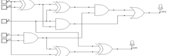
In our ALU we have used the concept of adder-subtractor where the same circuit performs the functions of both adder and subtractor as shown in fig 2.2. The adder functions based on the concept of look ahead carry adder. The subtractor just uses an xor gate as an extra circuitry.
The block diagram for an adder-subtractor circuit thus can be as below. To perform this we used carry look ahead adder, The carry look ahead adder reduces the consumption of power without compromising the speed of the adder[2]. This is achieved by generating carry simultaneously from all the bits. An n-bit carry look-ahead adder is formed from n stages. Carry look-ahead can be extended to larger adders. For example, four 1bit adders can be connected to form a 4bit adder and such four 4-bit adders can be connected to form the 16-bit adder.
Fig 2.2: Adder/Subtractor Unit
The use of a single circuit for both adder and subtractor reduces power consumption and also area. The operation of the adder-subtractor is based on the S1 and S0 control bits.
Table 2.2: Operations of adder/subtractor circuit
S1 S0 Operation
0 0 Half Adder
0 1 Half Subtractor
1 0 Full Adder
1 1 Full Subtractor
b. Logic Unit:
Fig 2.3 shows the logic unit in ALU, which performs 4 different logical operations AND, OR, XOR and NOT operations. Bitwise operation is performed on the two inputs. The operation to be performed is decided by two selections s1 and so as shown in Table 2.3.
Table 2.3: Logical Operations
C. Shifter Unit:
Logical shift is an efficient way to perform division and multiplication of integers by powers of two. Shifting left by k bits on a binary number is equivalent to multiplying it by 2k.Similarly shifting right by k bits on an binary number is equivalent to dividing it by 2k.
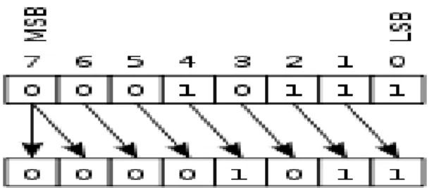
For example, consider the binary number 0001 0111.
C.1 Arithmetic shifts
Arithmetic shifts can be useful as efficient ways of performing multiplication or division of signed integers by powers of two. Shifting left by n bits on a signed or unsigned binary number has the effect of multiplying it by 2n. Shifting right by n bits on a two's complement signed binary number has the effect of dividing it by 2n, but it always rounds down (towards negative infinity).
Arithmetic left shift [6] move bits to the left, same order throw away the bit that pops off the MSB introduce a 0 into the LSB. This is same as logical left shift. It is shown in figure 2.4.a. Arithmetic right shift move bits to the right, same order throw away the bit that pops off the LSB reproduce the original MSB into the new MSB as shown in figure 2.4.b.
Fig 2.4.a:
Arithmetic Left Shift
Fig 2.4.b:
Arithmetic Right Shift
C.2 Logical Shifts
:
Logical shift is a bitwise operation that shifts all the bits of its operand. The two base variants are the logical left shift and the logical right shift. This is further modulated by the number of bit positions a given value shall be shifted, like "shift left by 1" or a "shift right by n". Unlike an arithmetic shift, a logical shift does not preserve a number's sign bit or distinguish a number's exponent from its mantissa; every bit in the operand is simply moved a given number of bit positions, and the vacant bit-positions are filled in, usually with zeros [7].
Logical left shift move bits to the left, same order throw away the bit that pops off the MSB introduce a 0 into the LSB as shown in figure 2.5.a. Logical right shift move bits to the right, same order throw away the bit that pops off the LSB introduce a 0 into the MSB as shown in figure
2.5.b.
Fig 2.5.a:
Logical Left Shift
Fig 2.5.b:
Logical Right Shift
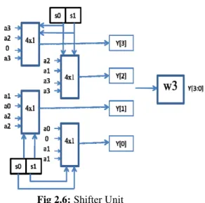
Fig 2.6 shows the diagram of Shifter unit which performs arithmetic/Logical ,Right and Left shifts by using Multiplexer and table 2.4 shows shifter operations controled by 2 selection lines s1 and s0.S1 S0 Operation
0 0 AND
0 1 OR
1 0 XOR
Fig 2.6:
Shifter Unit
Table 2.4: Shifter unit Operations
D. Multiplier Unit:
The multiplication algorithm for an N bit multiplicand by N bit multiplier is shown below, AND gates are used to generate the Partial Products, PP, If the multiplicand is N-bits and the multiplier is M-bits then there is N* M partial product. The way that the partial products are generated or summed up is the difference between the different architectures of various multipliers. Multiplication of binary numbers can be decomposed into additions. Consider the multiplication of two 8-bit numbers A and B to generate the 16 bit product P.
1. If the LSB of Multiplier is „1‟, then add the multiplicand into an accumulator.
2. Shift the multiplier one bit to the right and multiplicand one bit to the left.
3. Stop when all bits of the multiplier are zero. Speed of the Processor mainly depends on
Multiplier performance. There are Several
Techniques for design of Multipliers. We need to select the appropriate technique based on factors delay, throughput, area and design complexity.
Here we used array multiplier in my ALU. An array multiplier is a digital combinational circuit that is used for the multiplication of two binary numbers by employing an array of full adders and half adders. This array is used for the nearly simultaneous addition of the various product terms involved. The Hardware requirement for an m x n bit array multiplier is (m x n) AND gates, (m-1)x n Adders in which n HA(Half Adders) and (m-2)xn FA(full adders).
Figure 2.7 shows 4x4 array multiplier which uses 16 AND gates, 12 adders in which 4 Half Adders and 8 full adders. In the same way we can extend this to 8 bit. The multiplication of two 8 bit numbers results in 16 bits.
Fig 2.7: 4x4 Array Multiplier
III. INTRODUCTION TO REVERSIBLE
LOGIC GATES:
Several reversible gates have come out in the recent years. The most basic reversible gate is the Feynman gate and is shown in Fig 3.1. It is the only 2x2 reversible gate available and is commonly used for fan out purposes. Consider the input B as constant. When B is zero, the gate acts as a copying gate or a buffer where both the output lines contain the input A. When B is one, the complement of A is obtained at the output Q. The 3x3 reversible gates include Toffoli gate, Fredkin gate, New gate and Peres gate, all of which can be used to realize various Boolean functions. Fredkin gate is shown in Fig.3.2.The 4x4 reversible gates include TSG gate, MKG gate, HNG gate, PFAG gate etc[4].
Fig.3.3 shows the TSG gate. Some of the 4x4 gates are designed for implementing some important combinational functions in addition to the basic functions. Most of the above mentioned gates can be used in the design of reversible adders.
S1 S0 Operation
0 0 No shift
0 1 Arithmetic/Logical Left Shift
1 0 Logical Right Shift
3.1 Feynman Gate (CNOT)
Feynman gate (Controlled gates) act on 2 or more input bits, where one or more input bits act as a control for some operation. For example, the controlled NOT gate (or CNOT) acts on 2 input bits, and performs the NOT operation on the second input bit only when the first input bit is on or binary 1, and otherwise leaves it unchanged. It is represented by
Fig 3.1: Feynman Gate
3.2 Toffoli Gate
The Toffoli gate, also CCNOT gate, is a 3-bit gate, which is universal for classical computation. The quantum Toffoli gate is the same gate, defined for 3 input bits
.
If the first two bits are in the on state or binary „1‟, it applies a complement on the third bit, else it does nothing. It is an example of a controlled gate. Since it is the quantum analog of a classical gate, it is completely specified by its truth table 3.1.
Table 3.1: Truth table of Toffoli gate
A
B
C
P
Q
R
0
0
0
0
0
0
0
0
1
0
0
1
0
1
0
0
1
0
0
1
1
0
1
1
1
0
0
1
0
0
1
0
1
1
0
1
1
1
0
1
1
1
1
1
1
1
1
0
Fig 3.2: Toffili gate
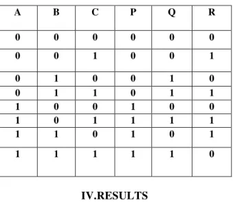
3.3 Fredkin Gate
The Fredkin gate (also CSWAP gate) is a 3-bit gate that performs a controlled swap. It is universal for classical computation. It has the useful property that the numbers of 0s and 1s are conserved throughout, which in the billiard ball model means the same number of balls are output as input.
Fig 3.3: Fredkin Gate
Table 3.2: Truth Table of Fredkin Gate
A B C P Q R
0 0 0 0 0 0
0 0 1 0 0 1
0 1 0 0 1 0
0 1 1 0 1 1
1 0 0 1 0 0
1 0 1 1 1 1
1 1 0 1 0 1
1 1 1 1 1 0
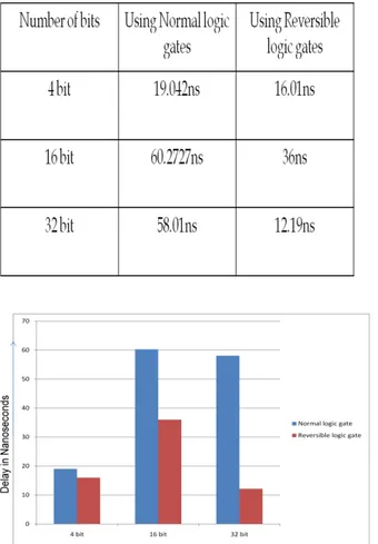
IV.RESULTS
4.1 DELAY RESULT FOR 4, 8 AND 16 BIT ALU
Table 4.1: Delay Table
Fig 4.1: Delay graph between reversible and normal
ALU
4.2 Simulation Output
V. CONCLUSION AND FUTURE SCOPE:
Hence the delay generated by using reversible logic gate has decreased drastically as the bit size increased in the input side in compare with normal logic gates. Though hardware area has increased by a small in number, it can be further improved by designing using combination of reversible logic gates.
The proposed ALU is using 16 bit for arithmetic block, logic block and shifter block. And 8 bit for array multiplier. This expansion can also be implemented for higher bits as a result we get very less delay period.
REFERENCES:
[1] Landauer, R., “Irreversibility and heat generation in the computing process”, IBM J.Research and Development, vol. 5 (3): pp. 183-191, 1961.
[2] Bennett, C.H., “Logical reversibility of computation”, IBM J. Research and Development, vol. 17: pp. 525-532, 1973. [3] B. Raghu Kanth1, B. Murali Krishna2, G.
Phani Kumar3, J. Poornima4, K. Siva Rama Krishna “ A Comparitive Study Of Reversible Logic Gates”International Journal of VLSI & Signal Processing Applications, Vol.2,Issue 1, Feb 2012.
[4] Himanshu Thapliyal ,Nagarajan Ranganathan “A New Reversible Design of BCDAdder ” IEEE conference on Design and automation, 2011 pp.1-4.
[5] Zhijin Guan, Wenjuan Li, Weiping Ding, Yueqin Hang, Lihui Ni“An Arithmetic Logic Unit design based on reversible logic gates ”IEEE Pacific Rim Conference on Communications, Computers and Signal Processing (PacRim), 2011.
[6] Thapliyal H, Srinivas M.B, “Novel Reversible TSG Gate and Its Application for
Designing Components of Primitive
Reversible/Quantum ALU,”Fifth International Conference on Information, Communications and Signal Processing, 2006.
[7] H.Thapliyal,M.B Srinivas “Novel design and