Performance Analysis of Reversible Fast Decimal
Adders
Rekha K. James, Shahana T. K., K. Poulose Jacob, and Sreela Sasi
Abstract -This paper presents a performance analysis of
reversible, fault tolerant VLSI implementations of carry select and hybrid decimal adders suitable for multi-digit BCD addition. The designs enable partial parallel processing of all digits that perform high-speed addition in decimal domain. When the number of digits is more than 25 the hybrid decimal adder can operate 5 times faster than conventional decimal adder using classical logic gates. The speed up factor of hybrid adder increases above 10 when the number of decimal digits is more than 25 for reversible logic implementation. Such high-speed decimal adders find applications in real time processors and internet-based applications. The implementations use only reversible conservative Fredkin gates, which make it suitable for VLSI circuits.
Index Terms- decimal arithmetic, delay reduction, reversible logic, VLSI implementation
I.
INTRODUCTIONCurrently, fast decimal arithmetic is gaining popularity in the computing community due to the growing importance of commercial, financial, and internet-based applications, which normally process decimal data. Low power designs with high performance are given prime importance by researchers, as power has become a first-order design consideration. While efforts are being made to reduce power dissipation due to leakage currents, alternate circuit design considerations are also gaining importance. In recent years, reversible logic has emerged as one of the most important approaches for power optimization. Landauer’s principle states that a heat equivalent to kT*ln2 is generated for every bit of information
lost, where k is the Boltzmann’s constant and T is the
temperature [1]. Bennett showed that energy dissipation would not occur if the computations were carried out using reversible circuits [2] since these circuits do not lose information. Classical logic gates such as AND, OR, and XOR are not reversible. Hence, these gates dissipate heat and may reduce the life of the circuit. So, reversible logic is in demand in high-speed power aware circuits.
Manuscript received July 4, 2007.
Rekha K. James is with Division of Electronics, Cochin University of Science and Technology, Kochi, Kerala-682022, India (phone: 0091-484-2320212; e-mail: rekhajames@ cusat.ac.in).
Shahana T. K., is with Division of Electronics, Cochin University of Science and Technology, Kochi, Kerala, India. (e-mail: [email protected]).
Dr. K. Poulose Jacob is with Department of Computer Science, Cochin University of Science and Technology, Kochi, Kerala, India (e-mail: [email protected]).
Dr. Sreela Sasi is with the Computer Science Department, Gannon University, Erie, PA, USA. (e-mail: [email protected]).
A reversible conventional Binary Coded Decimal (BCD) adder is proposed in [3] using NG (New Gate) and NTG (New Toffoli Gate) reversible gates. Even though the implementation is modified in [4] using TSG reversible gates, this approach is not taking care of the fanout restriction of reversible circuits, and hence it is only a near-reversible implementation. An improved reversible implementation of decimal adder with reduced number of garbage outputs is proposed in [5]. These implementations are for the conventional BCD adders, which are relatively slow.
Parity checking is one of the oldest and the most widely used methods for error detection in digital systems. Parity preservation proves to be useful for ensuring the robustness of reversible logic circuits. Parity-preserving reversible logic gates can be used for fault detection. B. Parhami demonstrated the feasibility of parity-preserving approach in the design of reversible logic circuits with examples of adder circuits [6].
In this research, carry select and hybrid decimal adders suitable for multi-digit BCD addition are implemented using parity preserving reversible Fredkin gates. Fredkin gates are conservative reversible gates. A gate is conservative if the Hamming weight (number of logical ones) of its input equals the Hamming weight of its output. If a gate is conservative and reversible then it is parity preserving.
The organization of this paper is as follows: Initially, fast decimal adders such as carry select and hybrid adders are described. A comparison of carry select and hybrid BCD adders with conventional decimal adder in terms of speed and area is done for classical gate implementation. Next section describes implementations of carry select and hybrid adders using only parity preserving reversible Fredkin gates. An optimum block size for a hybrid adder is also derived. Finally, a graphical delay analysis of different fault tolerant implementations normalized to a Fredkin gate is presented.
II. CARRY SELECT BCD ADDER
The carry select BCD adder shown in Fig. 1 consists of a 4-bit binary adder, a 6-correction circuit, and a modified special adder along with a circuit (2-input AND, 2-input OR and a 2:1 multiplexer) to generate decimal carry out (dcout).
The 4-bit binary adder adds the BCD inputs and generates a binary sum, S (S3-0) that is checked by the ‘6-correction
circuit’.
The output of the 6-correction circuit ‘L’ is given as
Fig 1: Carry Select BCD adder
On receiving Cin, a K-bit can be generated using equation (2).
K = S3S0Cin + L = P0Cin + L (2)
where P0 is the carry propagate signal (S3S0)
If the carry select technique is adopted for K-bit generation then k1 denotes the K-bit with Cin = 1 and k0 with Cin = 0 and
is given by k1=P0+L and k0=L. After computing both bits (k1
and k0) a selection is done using a 2:1 multiplexer.
To reduce the hardware and to increase the speed of the circuit, the final adder stage (4-bit special adder) is a modified version of a 4-bit binary adder consisting of a half adder, 2 full adders and an XOR gate as in Fig. 1.
An N-digit carry select adder will have a total (worst case) delay (Tdsum (carry-select)) equal to the sum of the ‘carry delay’
through the first digit (Tdcout(carry-select)), the carry select delays
through the next (N-1) digits, and the ‘sum delay’ through the last digit (Tsum-digit(carry-select)). This is given in equation (3).
Tdsum(carry-select) =
Td-cout(carry-select)+(N-1)Tmux+Tsum-digit(carry-select) (3)
where Tdcout(carry-select) is the delay to generate K-bit from the
BCD inputs for the first digit Tmux is the delay of a 2:1 multiplexer
Tsum-digit(carry-salact) is the delay of special adder for last
digit
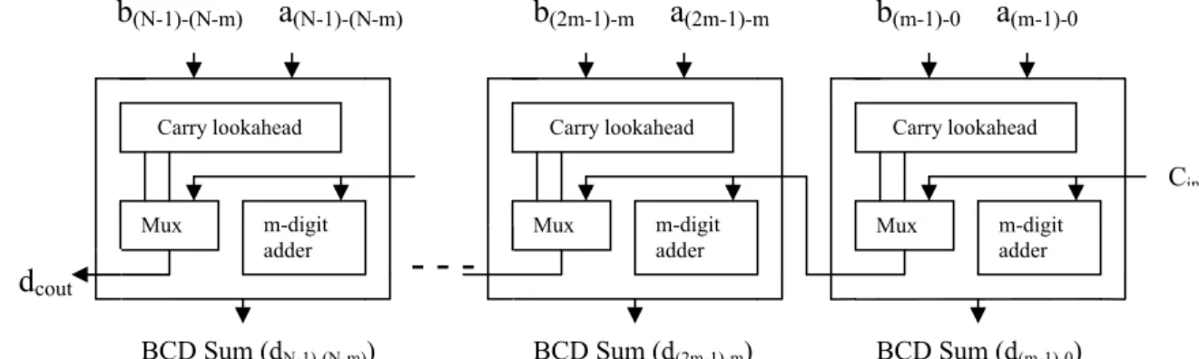
III. HYBRID BCD ADDER
Hybrid logic for N-digit BCD addition can be used for delay reduction and is shown in Fig.2. The N-digit BCD input is divided into m-digit fixed blocks. Each m-digit adder consists of ‘m’ single digit carry select adders. To speed up addition, carry lookahead logic is included in m-digit blocks. For an m-digit adder, Decimal Cout at mth digit (Km-1) can be
computed as given in equation (4) using equation (2).
m-1 m-1 m-1
Km-1 = Cin∏ Pk + ∑ Li [ ∏ Pj ] (4) k=0 i=0 j=i+1
where Li is the L-bit of ith digit
Pi is the propagate bit for ith digit
This can be written as
Km-1 = k0(m-1) Cin’ + k1(m-1) Cin (5)
where k0(m-1) = Km-1 with Cin = 0
k1(m-1) = Km-1 with Cin =1
The computations up to the generation of Li and Pi bits at
each digit are carried out in parallel for all digits. The delay for L-bit generation is given as
TL = Tadder + T6-correction (6)
where Tadder is the delay of the 4-bit binary adder,
T6-correction is the delay of the 6-correction circuit
k0(m-1) and k1(m-1) for an m-digit block are computed using
Li and Pi as given in equation (4) after a delay of Tk1(m-1)
which is the delay of an m-input AND gate and (m+1) input OR gate.
Fig 2. Hybrid N-digit Decimal Adder
m-digit adder Carry lookahead
Mux m-digit
adder Carry lookahead
Mux
-BCD Sum (d(m-1)-0)
BCD Sum (d(2m-1)-m)
Cin
b
(m-1)-0a
(m-1)-0b
(2m-1)-ma
(2m-1)-mm-digit adder Carry lookahead
Mux
BCD Sum (dN-1)-(N-m))
b
(N-1)-(N-m)a
(N-1)-(N-m)On receiving Cin, the Decimal Cout at mth digit (Km-1) is
generated after an additional delay of a 2:1 multiplexer (Tmux)
and is given as
Tm-dcout = TL + Tk1(m-1) + Tmux (7)
The total (worst case) delay of an N-digit hybrid BCD adder (Tdsum (hybrid)) with fixed size carry look ahead block is
the sum of the ‘carry delay’ through the first m-digit lookahead adder block (Tm-dcout), the carry select delays
through the intermediate blocks, and the ‘sum delay’ through the last m-digit block (Tsum-m-digit ). This is given in equation
(8).
Tdsum (hybrid) = Tm-dcout + [(N/m)-2] Tmux + Tsum-m-digit (8)
where Tsum-m-digit = mTmux+ Tsum-digit (9)
The total (worst case) delay of an N-digit conventional BCD adder (Tdsum (conventional)) given in equation (10) is the sum
of ‘N’ times the ‘carry delay’ through one digit and the ‘sum delay’ through the last digit (Tsum-digit(conventional)).
Tdsum (conventional) = N Tdcout(conventional)+ Tsum-digit(conventional) (10)
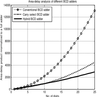
A comparison of conventional, carry select and hybrid (with m=4) BCD adders in terms of area and critical path delay is done with the logic synthesis tool Leonardo Spectrum from Mentor Graphics Corporation using ASIC Library. The critical path delay and area are normalized with respect to a full adder critical path delay of 1.98 ns and area of 38μm2
. Fig. 3 shows the graphical analysis of delay, and Fig. 4 shows the area-delay product normalized to that of a full adder. The area overhead of carry select and hybrid adders is compensated by the speed advantage compared to the conventional adder.
0 5 10 15 20 25 0
10 20 30 40 50 60 70
No: of digits
D
e
la
y
n
o
rm
a
li
z
e
d
t
o
a
f
u
ll
a
d
d
e
r
Delay analysis of different BCD adders Conventional BCD adder
Carry Select BCD adder Hybrid BCD adder
Fig. 3: Delay analysis of Conventional, Carry Select and Hybrid BCD Adders
0 5 10 15 20 25 0
2000 4000 6000 8000 10000 12000 14000
No: of digits
A
re
a
-d
e
la
y
p
ro
d
u
c
t
n
n
o
rm
a
li
z
e
d
t
o
a
f
u
ll
a
d
d
e
r
Area-delay analysis of different BCD adders Conventional BCD adder
Carry select BCD adder Hybrid BCD adder
Fig. 4: Analysis of area-delay product of Conventional, Carry Select and Hybrid BCD Adders
Fig. 5 demonstrates the speed up factor of carry select and hybrid BCD adders compared to conventional BCD adder as the number of digits increases. Hybrid decimal adder is three times faster than the conventional BCD adder as the number of digits increases above 12 while the carry select BCD adder attains a speed up factor of 2.5 at this level. It is noted that the hybrid adder attains speed up over carry select BCD adder only when the number of input digits increases above 8. The delay comparison graphs show that hybrid adder is 5 times faster than that for the conventional BCD adder, when the input word length is above 25.
0 5 10 15 20 25
0 0.5 1 1.5 2 2.5 3 3.5 4 4.5 5
No: of digits
S
p
e
e
d
u
p
f
a
c
to
r
Speed improvement for Carry select and Hybrid BCD adders
Carry select vs. Conventional BCD adder Hybrid vs. Conventional BCD adder
IV. REVERSIBLE GATES
This section describes parity preserving reversible logic gates such as Feynman Double Gate (F2G) and Fredkin Gate (FRG). A 3*3 Feynman Double Gate (F2G) [6] has 3 inputs A, B, C and 3 outputs P=A, Q=A B, R=A C. A 3*3 Fredkin Gate (FRG) [7] has 3 inputs A, B, C and 3 outputs P=A, Q=A’B AC, R= AB A’C. These two gates satisfy the condition A B C=P Q R. In general, a parity preserving reversible gate is a gate in which the following condition is valid.
∑Xi = ∑Yi (11)
where ‘X’ indicates an input, ‘Y’, an output, and ‘i’ the number of inputs or outputs of the reversible gate.
V. PARITY PRESERVING REVERSIBLE CARRY SELECT BCD ADDER
Recently, Hafiz [3], Thapliyal [4] and James [5] proposed reversible implementations of conventional BCD adders. But these implementations make use of reversible gates other than parity preserving gates, and hence they are not fault tolerant implementations. This research proposes a reversible implementation of fast BCD adders using the parity preserving reversible Fredkin gates.
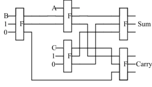
The basic component of any adder is a full adder. A number of parity preserving reversible full adders are available in literature [6, 8]. Fig. 6 and Fig. 7 show the implementation of a half adder and a full adder using parity preserving Fredkin gates. The full adder implementation requires only 5 Fredkin gates at 3 levels, compared to 3-level 6-gate (5 Fredkin gates and 1 Feynman gate) implementation in [6], and level 5-Fredkin gate implementation in [8] while observing the fanout restrictions.
The 4-bit binary adder realized using a half adder and 3 full adders will achieve delay reduction by using implementations in Fig. 6 and Fig. 7. The least significant bit (half adder) requires a path delay of two FRGs to generate C0 from the
addends. Then the carry ripples through the subsequent full adders with a path delay of two FRGs per bit. This is because the first Fredkin gates of all full adders work in parallel with the first Fredkin gate of half adder in an n-bit binary adder. But in the implementation in [6], the delay is of 3 levels for each bit. So, an advantage of 1 delay level/bit is achieved in this implementation. The delay to generate Cout or ‘Sum’ in
the n-bit binary adder is
Tc-ripple = Tsum-ripple = 2+2(n-1) (12)
Fig. 6: Half adder using Fredkin Gates
Fig. 7: Full adder using Fredkin Gates
For a conventional n-bit adder with ‘n’ full adders, it is
T c-ripple (conventional) = Tsum-ripple(conventional) = 3+2(n-1) (13)
For a BCD adder this delay is the delay with n=4 for each digit. In carry select BCD adder, since all digits are added in parallel this delay remains the same as a single digit for ‘N’ digit addition.
The parity preserving reversible implementation of a 6-correction circuit is shown in Fig. 8. The implementation requires 3 FRGs to generate the ‘L’ output. This circuit takes only 2 more delays after generating the ‘Sum’ to generate the L-bit. The delays to generate L-bit from the BCD inputs for carry select and conventional BCD adders are given in (14) and (15).
TL(carry-select) = 4+2(n-1) (14)
TL (conventional) = 5+2(n-1) (15)
Fig. 9 shows the generation of K-bit or the Decimal Cout.
The generation of k1 and k0 takes the delay of only one
Fredkin gate after receiving L-bit as seen in Fig. 9. After computing both values (k1 and k0) a selection is done by a
single FRG, since an FRG works as a 2:1 multiplexer with ‘A’ input as control input and ‘B’ and ‘C’ inputs as data inputs. So, the additional delay in each digit to generate K-bit after receiving Cin is only due to one FRG.
Fig. 8: Generation of L-bit using Fredkin Gates
Fig. 9: Generation of K-bit using k0 and k1
F F
A 0 B
1 0
F
AB=Carry
A B=Sum
A F
C 1 0
F
Carry Sum F F
B 1 0
F
F F
F S1
S2
1 L
S3
0 1
S3 Cout
F
F S3
S0 0
S3 L
1
K=Decimal Cout F
k0 k1
The delay in generation of K-bit (Decimal Cout) for one
digit for carry select BCD adder is given in equation (16), where n=4.
Td-cout(carry-select) = 6+ 2(n-1) (16)
Special adder implemented using one half adder, two full adders and one XOR gate requires 15 Fredkin gates (3 for half adder, 5 for each full adder, 2 for XOR gate) to generate the BCD sum (d3-0). The Decimal Cout or the K-bit is the last input
to be received for the special adder. The ‘K’ input passes through a maximum of 5 Fredkin gates to generate the BCD sum (d3-0). But Cin is received by the special adder along with
the K-bit only. On receiving Cin the half adder of the special
adder generates the carry bit after one Fredkin gate delay. The 2 full adders and one XOR gate adds 5 more Fredkin gate delays. So the delay of special adder (Tsum-digit(carry-select) ) is the
delay of 6 Fredkin gates.
For an N-digit BCD adder, Decimal Cout at Nth digit (K(N-1))
is generated after a delay equal to the sum of delay of K-bit generation for the first digit (Tdcout(carry-select))and the
multiplexer delays through the next (N-1)digits. It is given in equation (17).
TN-d-cout(carry-select) = Tdcout(carry-select)+(N-1)Tmux
= 6+2(n-1) + (N-1) (17)
Substituting the delays in equation (3), the total worst case delay (Tdsum (carry-select)) in terms of Fredkin gate delay is
Td-sum (carry-select) = 6+2(n-1) + (N-1) + 6 (18)
For a conventional BCD adder the final adder is a 4-bit binary adder. The ‘K’ input passes through a maximum of 6 Fredkin gates (3 full adders) of the final adder to generate the BCD sum. So total (worst case) delay of an N-digit conventional BCD adder in terms of Fredkin gate delay is
T d-sum (conventional) = N Tdcout(conventional) + Tsum-digit (conventional)
= N TL(conventional) + Tsum-digit(conventional)
= (5+2(n-1)) N + 6 (19)
VI. HYBRID REVERSIBLE BCD ADDER
The total (worst case) delay of an N-digit hybrid BCD adder with fixed size carry look ahead block is given in equation (8). The first term in equation (8) requires a delay as given in equation (7). In reversible implementation using Fredkin gates the delay to generate all Li bits is TL (given in
equation (14)) with n=4. All Pi will be available when the
generation of Li gets over. Tk1(m-1) is the delay of an m-input
AND gate and (m+1) input OR gate. A 2 input AND or a 2 input OR can be implemented by a single Fredkin gate. Higher order AND and OR gates can be constructed using Fredkin gates arranged in a binary tree. An m-input AND gate or an m-input OR gate requires (m-1) Fredkin gates. In a binary tree implementation an input passes through a maximum of
m
2
log
Fredkin gates [8]. On receiving Cin,the selection of k1(m-1) or k0(m-1) requires one more Fredkin
delay for each m-digit block. Hence the ‘carry delay’ through the first m-digit lookahead adder block is
Tm-dcout = 10 +
log
2m
+
log
2(
m
1
)
+ 1 (20)The delay for carry select for intermediate blocks is
m
N
- 2.
The sum delay through the last m-digit block is (m+6). Total delay in generating N-digit BCD sum is given as
Td-sum (hybrid) =
11+
m
2log
+
log
2(
m
1
)
+m
N
-
2 + m+6 (21)However, the assumption
m
2log
=2
m
is valid for the
small block sizes applicable to carry look ahead adder designs. Thus, (21) can be written as
Td-sum (hybrid) = 15+2m+
m
N
(22)
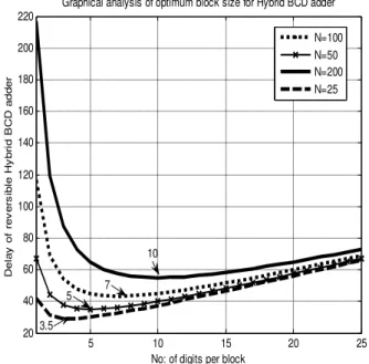
Minimizing Td-sum (hybrid) with respect to block size m
mopt=
0
.
5
N
(23)Substituting (23) into (22) gives the shortest delay for a fixed block size hybrid BCD reversible adder.
Td-sum (hybrid) = 15 +
8
N
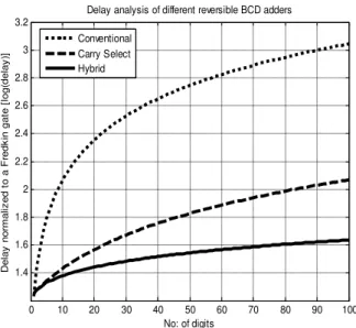
(24)Fig. 10 graphically demonstrates the computation of optimum block size (corresponding to shortest delay) of hybrid reversible BCD adders for different input lengths. Fig. 11 shows a comparative delay analysis of conventional, carry select and hybrid BCD adder reversible implementations normalized to that of a Fredkin gate.
5 10 15 20 25
20 40 60 80 100 120 140 160 180 200 220
No: of digits per block
D
e
la
y
o
f
re
v
e
rs
ib
le
H
y
b
ri
d
B
C
D
a
d
d
e
r
Graphical analysis of optimum block size for Hybrid BCD adder
N=100 N=50 N=200 N=25
10
7 5
3.5
0 10 20 30 40 50 60 70 80 90 100 1.4
1.6 1.8 2 2.2 2.4 2.6 2.8 3 3.2
No: of digits
D
e
la
y
n
o
rm
a
li
z
e
d
t
o
a
F
re
d
k
in
g
a
te
[
lo
g
(d
e
la
y
)]
Delay analysis of different reversible BCD adders
Conventional Carry Select Hybrid
Fig. 11: Delay analysis of VLSI implementations of BCD adders
Figure 12 demonstrates the speed up factor of reversible Fredkin gate implementations of carry select and hybrid BCD adders compared to conventional BCD adder. It can be noted that the hybrid adder attains speed over carry select BCD adder for all values of N in reversible implementation. Speed up factor of hybrid adder increases above 10 when the number of decimal digits is more than 25 for fault tolerant reversible logic implementation.
VII. CONCLUSION AND FUTURE WORK
This research forms the basis of a fast Decimal ALU for a reversible CPU. Faster decimal adder circuits have been explored for several decades. This paper continues that practice by describing several reversible BCD adders using only Fredkin gate (FRG), a conservative reversible logic gate. VLSI implementations using only one type of modular building blocks can decrease system design and manufacturing cost.
0 10 20 30 40 50 60 70 80 90 100
0 5 10 15 20 25 30
No: of digits
S
p
e
e
d
u
p
f
a
c
to
r
Speed improvement of Carry select and Hybrid reversible BCD adders
Carry select vs Conventional Hybrid vs Conventional
Fig. 12: Speed up factor for VLSI reversible implementations of fast BCD adders vs. Conventional BCD adder
The performance comparison of carry select and hybrid BCD adders with conventional BCD adder are presented. It is noted that the hybrid BCD adder attains speed up over carry select and conventional BCD adders, for any input length in a reversible implementation.
Varying the size of the carry lookahead blocks can reduce the total worst case delay, since carries generated or absorbed in the adder center have shorter data paths [9]. Investigations into determining alternate implementations can be done using logic synthesis methods [10, 11, 12]. Characterization of new families of ‘n-input’ – ‘n-output’ reversible gates that can be used for regular structures is an area which can be investigated further. Additionally, it is noted that there is a lack of simulation tools that support reversible gates, and this is most definitely an area worthy of attention.
REFERENCES
[1] R. Landauer, “Irreversibility and Heat Generation in Computational Process”, IBM Journal of Research and Dev., 5, pp.183-191, 1961. [2] Bennett, C., “Logical Reversibility of Computation,” IBM Journal of
Research and Development, 17, pp.525-532, 1973.
[3] Md. Hafiz Hasan Babu and A. R. Chowdhury, "Design of a Reversible Binary Coded Decimal Adder by Using Reversible 4-bit Parallel Adder”, VLSI Design ‘05, pp.255-260, Jan 2005.
[4] H. Thapliyal, S. Kotiyal and M.B Srinivas, “Novel BCD Adders and their Reversible Logic Implementation for IEEE 754r Format”, 19th VLSI Design 2006, pp. 387-392, Jan 2006.
[5] R. James, T. K. Shahana, K. P. Jacob and S. Sasi, “Improved Reversible Logic Implementation of Decimal Adder”, To be published in Proceedings of IEEE 11th VDAT Symposium Aug, 2007.
[6] B. Parhami; “Fault Tolerant Reversible Circuits” Proc. 40th Asilomar Conf. Signals, Systems, and Computers, CA, Oct 2006.
[7] E. Fredkin and T. Toffoli, “Conservative logic”, Intl. J. Theoretical Physics, Vol 21, 1982, pp. 219-253.
[8] J.W.Bruce, M.A.Thornton, L.Shivakumariah, P.S.Kokate, X.Li, "Efficient Adder Circuits Based on a Conservative Logic Gate", Proceedings of the IEEE Computer Society Annual Symposium on VLSI, April 2002, PA, USA, pp 83-88.
[9] B. Parhami, Computer Arithmetic: Algorithms and Hardware Designs, Oxford University Press, 2000.
[10] Dmitri Maslov, "Reversible Logic Synthesis”, PhD Dissertation, Computer Science Department, University of New Brunswick, Canada, October 2003.
[11] P. Gupta, A. Agrawal, N. K. Jha, “An algorithm for synthesis of reversible logic circuits”, IEEE Transactions on Computer Aided Design of Integrated Circuits and Systems”, Nov. 2006, Volume: 25, Issue 11, pp. 2317-2330.