w w w . a j e r . o r g
Page 87
American Journal of Engineering Research (AJER)
e-ISSN : 2320-0847 p-ISSN : 2320-0936
Volume-03, Issue-12, pp-87-92
www.ajer.org
Research Paper Open Access
A Novel Design of Half Subtractor using Reversible Feynman
Gate in Quantum Dot cellular Automata
Rubina Akter
1,Nasrin Jahan
2, Md. Mamunur Rashid Shanta
3, Anik Barua
41, 4(Department of ICT, MawlanaBhasani Science and Technology University, Bangladesh) 2
(Department of TE, University of South Asia, Bangladesh)
3(Department of EEE, East West University, Bangladesh)
Received Manuscript: XX-XX-XXXX Accept Manuscript: XX-XX-XXXX Published Manuscript: XX-XX-XXXX
ABSTRACT:
Quantum Dot cellular Automata (QCA) is an emerging, promising alternative to CMOStechnology that performs its task by encoding binary information on electronic charge configuration of a cell. All circuit based on QCA has an advantages of high speed, high parallel processing, high integrityand low power consumption. Reversible logic gates are the leading part in Quantum Dot cellular Automata. Reversible logic gates have an extensive feature that does not lose information. In this paper, we present a novel architecture of half subtractor gate design by reversible Feynman gate. This circuit is designedbased on QCA logic gates such as QCA majority voter gate, majority AND gate, majority OR gate and inverter gate. This circuit will provide an effective working efficiency on computational units of the digital circuit system.
Keywords
-
And-Or-Inverter (AOI), Basic QCA, Majority Voter (MV), QCA Logic Gate, Reversible FeynmanGate.
I.
INTRODUCTION
The paradigm of Quantum Dot cellular Automata is a revolutionary approach to molecular-scale computing. Using the charge configuration of nano structures Quantum Dot cellular Automata presents binary information on the current switching devices. For several decades the size of electronics semiconductor device and operating currents has been reduced. Fundamental problems arising from scaling such as quantum mechanical effects and severe power dissipations assist the continued development toward devices on the nanometer scale [1].
w w w . a j e r . o r g
Page 88
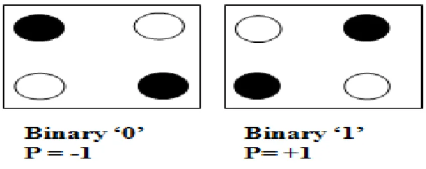
two stables positions known as -1 and +1 polarity or boolean values 0 and 1 respectively [6]. The presence of clocking zones is a unique feature of QCA based circuits. There are four phases of clocking zones such as the switch, hold, release and relax [7].
Now a day nanotechnology is one of the most wanted research field and Quantum Dot Cellular Automata offers a revolutionary approach to computing at nano level. Parallely, reversible logic is getting more and more conspicuous technology which offers better working performance in QCA technology. Previously researchers have addresseda number of studies on reversible logic gates and their implementation such as described in [8, 9, 10]. H. cho and j. Earl Swartzlander described adder and multiplier design that are optimized in terms of quantum cost, delay and garbage output [11]. A revolutionary design of a shift register and its operation is described in [5]. H. Thapliyal and N. Ranganathan proposed the design of binary and bcd adder circuits based on reversible logic gates. These designs are very effective in terms of reversible gates, garbage output and quantum cost [12]. I. Hanninen and J. Takala emphasis a binary adders design on QCA which is very important in arithmetic logic unit. The main parts is the implementation of logical devices and the reversible logic using QCA is shown in [13, 14].
There are many reversible logic gates and these gate are important for their reversibility characteristics. Among them Feynman gate is one of the most important reversible logic gates. In this paper using the reversible Feynman gate we design a Half Subtractor circuit. This design is very useful for digital signal processing (DSP), optical computing, cryptography etc.
This paper is apportioned into five sections. Section I describes about QCA, reversible logic gate and their implementation in various logical circuits. Section II provides a brief overview about the QCA fundamental logic units. Section III presents our proposed circuit using QCA technology. Section IV shows the simulated waveform and discuss about the simulation results of the proposed circuit. Finally, section V summed up the beneficial perspective of the presented circuit.
II.
QCA
R
EVIEWQuantum Dot cellular Automata is an outstanding nanotechnology which is used for its better performance than CMOS technology. We describe the basic building block of QCA cells in the previous section. A QCA cell is shown in figure 1. This figure is considered as a square with four dots as its corners. The cell is to consist of two extra electrons which can tunnel between cell dots [1, 15].
Figure 1: Structure of a QCA cell and its binary logic
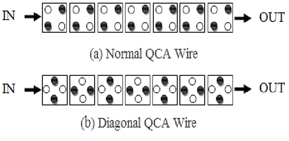
The QCA wire is basic QCA logic element which is consist of a set of QCA cells. Due to the
electrostatic repulsion signal propagates from input to output through the QCA wire. The QCA wire is a
w w w . a j e r . o r g
Page 89
Figure 2: QCA Wire
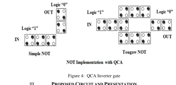
Another basic QCA logic elementis QCA majority Voter (MV) gate. The 3-input majority gate is composed
of five cells. The three cells act as input cell, the center cell is known as device cell and the remaining cell is
known as output cell. The center cell performs the calculations. Figure 3 shows a three input majority gates
where the input cells are labeled as A,B,C and the output cell labeled as OUT. The Boolean function of this
three input majority gate is,
OUT (A, B, C)=Maj (A, B, C)= AB+BC+CA.
The three input majority gate works as 2-input AND gate having a fixed polarity of zero and its output is ab.
The three input majority gate works as 2-input OR gate having a fixed polarity of 1 and its output is a+b.
Figure 3: QCA Majority Voter (MV) gate
w w w . a j e r . o r g
Page 90
Figure 4: QCA Inverter gate
III.
P
ROPOSEDC
IRCUIT ANDP
RESENTATIONThere are many reversible logic gates and these are extensively important to QCA technology. In this section we will present our proposed Halfsubtractor circuit which is implemented by reversible Feynman gate.
1. Feynman gate (FG)
Figure 5 shows a 2 x 2 Feynman gate. The input vector is I (A, B) and the output vector is O (P, Q) and the relation between input and output is given by P=A, Q =A⊕B.
Figure 5: Feynman gate
In this paper we design a reversible Half Subtractor circuit by Feynman gate using QCA Technology. Let A and B are two binary numbers. The half subtractor performs A-B operation. Table 2 shows the truth table of the half subtractor. The output of the XOR gate produces the difference between A and B. The output of the AND gate A'B produces a Borrow. Thus, the output function will be Borr = A'B, Diff = A⊕B.
Table 1: Truth Table of Half Subtractor
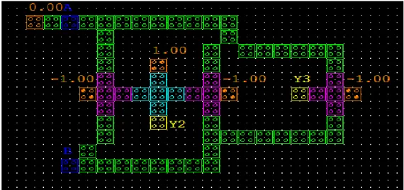
Figure 6 shows QCA layout structure of the Halfsubtractor design using reversible Feynman Gate. In this figure
the input cells are labeled with A and B and the outputs are labeled as Y2 and Y3. The circuit performs the
Boolean functions Y3 = Borr = A'B, Y2 = Diff = A⊕B.
Input Output
A B Borr Diff
0 0 0 0
0 1 1 1
1 0 0 1
w w w . a j e r . o r g
Page 91
Figure 6: Simulated waveforms for Half Subtractor gate by Feynman gate
IV.
R
ESULT ANDD
ISCUSSIONOur proposed Halfsubtractor circuit functionally simulated using the QCA Designer 2.0.3. The following
parameters are used for a Bistable Approximation: cell size=18nm, number of samples=12800, convergence
tolerance=0.0000100, radius of effect=65.000000nm, relative permittivity=12.900000, clock
high=9.800000e-022J, clock low=3.800000e–023J, clock shift=0, clock amplitude factor=2.000000, layer separation=11.500000,
Temperature=1.000000,Reluxation time=1.000000e-015, Time step 1.000000e-016 and Dot Diameter=5.0000.
Most of the above mentioned parameters are default values in QCA Designer. Figure 7 shows the input output
waveforms of our proposed circuit. In this Figure, the input signals are A, B and the output signals are Y3 and
Y2. The input is mapping to output as Y2 =A⊕B and borrow Y3=
A'B
.w w w . a j e r . o r g
Page 92
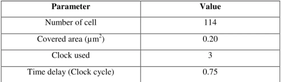
The table 2 shows a data table of Half Subtractor gate designingby Feynman gate.
Table 2:Result analysis of proposed half subtractor circuit in QCA
Parameter Value
Number of cell 114
Covered area (µm2) 0.20
Clock used 3
Time delay (Clock cycle) 0.75
The above tables show that, the Half Subtractor gate designing by Feynman gate consists of 114 cells and it covers 0.20 μm2 areas with time delay 0.75.
V.
C
ONCLUSIONThis paper explores a novel design of Half-Subtractor circuit based on the reversible Feynman gate using QCA technology. This proposed circuit has been simulated by QCADesigner. The simulation result shows that the proposed circuit produces the exact output and it performs well. The proposed design is more efficient in terms of cell counts, area and the time delay. This QCA circuit design presents a new functional paradigm for quantum computing, optical computing, digital signal processing and nanotechnology. Hence, we summarize that the proposed design architecture must be take a promising step towards the goal of low power dissipation circuit in QCA technology.
R
EFERENCES[1] C. S. Lent, P. D. Taugaw, W. Porod and G. H. Berstein, “Quantum Cellular Automata”, Nanotechnology, vol. 4, no. 1, January 1993, pp 49-57.
[2] Enrique P. Blair and Craig S. Lent, “Quantum-Dot Cellular Automata: An Architecture for Molecular Computing, ” 0 -7803-7826-1/03/$17.00 © 2003, IEEE.
[3] J. R. Zhang, K. Walus, W. Wang, and G. .Jullien, “A method of majority logic reduction for quantum cellular automata,” IEEE Transactions on Nanotechnology, vol. 3, no. 4, pp. 443–450, Dec. 2004.
[4] I. Hänninen and J. Takala, “Binary Adders on Quantum-Dot Cellular Automata,” J. Signal Process. Syst., vol. 58, no. 1, pp. 87–103, Jan. 2010.
[5] R. Kummamuru, A. Orlov, R. Ramasubramaniam, C. Lent, G. Bernstein, and G. Snider, “Op-eration of a quantum-dot cellular
automata (qca) shift register and analysis of errors,” IEEE Transactions on Apllied Physics, vol. 50, pp. 1906–1913, September 2003. [6] C. S. Lent and P. D. Tougaw, Proceedings of the IEEE 85, p. 541 (1997).
[7] Mohammad RafiqBeigh*, Mohammad Mustafa, Firdous Ahmad, “Performance Evaluation of Efficient XOR Structures in Quantum -Dot Cellular Automata (QCA), ” Circuits and Systems, 2013, 4, 147-156 .
[8] J. W. Bruce, M. A. Thornton, L. Shivakumaraiah, P. S. Kokate, and X. Li, “Efficient adder circuits based on a conservative reversible
logic gate,” in Proc. IEEE Symposium on VLSI, 2002, 2002, pp. 83–88.
[9] M. Haghparast, S. Jassbi, K. Navi, and O.Hashemipour, “Design of a novel reversible multiplier circuit using hng gate in
nanotechnology,” World App. Sci. J., vol. 3, no. 6, pp. 974–978, 2008.
[10] H. Thapliyal and M.B. Srinivas, “Novel reversible multiplier using novel reversible TSG gate,” in Proc.the 4th ACS/IEEE InternationalConference on Computer Systems and Applications, Dubai , UAE, 2006, pp. 100–103.
[11] H. Cho and J. Earl E. Swartzlander, “Adder and Multiplier Design in Quantum-Dot Cellular Automata,” IEEE Transactions on Computers, vol. 58, no. 6, pp. 721–727, 2009.
[12] H. Thapliyal and N. Ranganathan, “Design of efficient reversible logic based binary and bcd adder circuits,” To appear ACM Journal ofEmerging Technologies in Computing Systems, 2011.
[13] C.S Lent and B. Isaksen, “Clocked molecular quantum-dot cellular automata,” IEEE Trans. Electronic Devices, vol. 50, no. 9, pp. 1890-1896, Sept. 2003.
[14] P. D. Tougaw and C. S. Lent, “Logical devices implemented using quantum cellular automata,” Journal of Applied Physics, vol. 75, no. 3, pp. 1818–1825, Feb. 1994.
[15] RaghavaGaripelly, P.MadhuKiran, A.Santhosh Kumar, “A Review on Reversible Logic Gates and their Implementation,” ISSN 2250 -2459, ISO 9001:2008 Certified Journal, Volume 3, Issue 3, March 2013.
[16] Lent, Craig S., Tougaw, P. Douglas: Lines of interacting quantum-dot cells: A binary wire. Journal of Applied Physics. vol. 74 (1993), pp. 6227 – 6233.