David C. Wyld et al. (Eds) : ACITY, DPPR, VLSI, WiMNET, AIAA, CNDC - 2015
pp. 125–134, 2015. © CS & IT-CSCP 2015 DOI : 10.5121/csit.2015.51311
P. Koti Lakshmi
1, B Santhosh Kumar
2, Prof.Rameshwar Rao
31
Assistant Professor,Department of ECE, UCE,Osmania University, Hyderabad.
[email protected]2
Student, ME(ESVLSID), Department ofECE,UCE,Osmania University,
Hyderabad
[email protected]3
Professor(Retd) , Dept of ECE,UCE,Osmania University, Hyderabad.
[email protected]A
BSTRACTWith DSP applications evolving continuously, there is continuous need for improved multipliers which are faster and power efficient. Reversible logic is a new and promising field which addresses the problem of power dissipation. It has been shown to consume zero power theoretically. Vedic mathematics techniques have always proven to be fast and efficient for solving various problems. Therefore, in this paper we implement Urdhva Tiryagbhyam algorithm using reversible logic thereby addressing two important issues – speed and power consumption of implementation of multipliers. In this work, the design of 4x4 Vedic multiplier is optimized by reducing the number of logic gates, constant inputs, and garbage outputs. This multiplier can find its application in various fields like convolution, filter applications, cryptography, and communication.
K
EYWORDSMultipliers, Urdhva Tiryagbhyam algorithm, Reversible Logic, Vedic Multiplier, Optimization, Quantum cost.
1. INTRODUCTION
can be improved by optimizing the various parameter of the multiplier such as power, speed, area and fault tolerance property. Since these parameter are very much important for Reversible logic circuit or information lossless circuit has zero internal power dissipation and also there are few families of reversible gate that have inherent fault tolerant. This tolerant property in reversible circuit have application in variety of emerging technology such as quantum computing, nanotechnology etc. According to the Moore’s law ,by the 2020 the basic memory components of a computer will the size of the individual atoms. At such scales current theory of computer will be fail and an quantum computing reinvented the theory of computer science, Quantum computer can complete task in the breathtakingly time with no internal power dissipation. Multiplication process involves generation of partial products, addition of partial products and finally total product is obtained. So the performance of the multiplier depends on the number of partial products and the speed of the adder.
Vedic mathematics has 16 formulae for performing arithmetic calculation. An Urdhva Tiryakbahayam formula is used for he multiplication, application for all types for multiplication. its literal means “ Vertical and Cross-wise” which enhance the speed of multiplication operation. This paper deals with the survey and comparison of the various multiplier mainly in terms of the power, delay, quantum cost. From the survey it is find that the reversible Vedic multiplier based on the Urdhva tiryagbhyam aphorisms is offer the best results in terms of delay, area, power and quantum cost.
In the Array Multiplier ,generation of partial products and addition of that will take more time. Time is an important factor for any computing system. So, in this paper we are proposing the Vedic Multiplier which give results quicker than array multiplier and also Vedic Multiplier using reversible gates is designed with less TRLIC to decrease the power dissipation. In this paper we are also designing the signed vedic multiplier for multiplication of signed numbers.
Vedic Multiplier using reversible gates was proposed by different authors[2][3][4] and they had calculated TRLIC. In this paper we are designing the optimized Vedic multiplier and comparing with that. In this paper, we are discussing basic reversible gates, algorithm of 2x2 vedic multiplier and 4x4 vedic multiplier and how it is optimized by reducing number of gates, garbage outputs, quantum cost, constant inputs.
2. REVERSIBLE GATES
2.1. Reversible Logic Gates
2.1.1 Feynman Gate: It is 2x2 gate [3]. If the first input i.e. A is given as 1 the second output will be the complement of the second input i.e. B. so, this gate is also known as Controlled Not Gate. It can also be used to copy inputs. Quantum cost of this gate is one.
2.1.2 Peres Gate: It is a 3x3 gate [3]. It can be used as a half adder with third input i.e. c as 0.It also serves the purpose of fan out. Quantum cost of this gate is four.
2.1.4 BVPPG gate: In this 5x5 reversible gate [3] is proposed. It is basically for multiplication and can generate two partial products at a time. Quantum cost of this gate is ten.
The basic reversible gates are shown in Fig 1.
Fig.1 Reversible logic gates
3. MULTIPLICATION USING URDHVA TIRYAGBHYAM SUTRA
A Vedic maths offers two sutras – Urdhva Tiryagbhyam sutra and Nikhilam Sutra for multiplication. Nikhilam sutra is best used for numbers which are nearer to the base of 10,100, 1000 and increased power of 10, whereas Urdhva Tiryagbhyam can be used for any multiplication. The most powerful Vedic multiplication sutra Urdhva Tiryagbhyam means „Vertically and Crosswise”. This technique is applicable for any type of number system. General procedure for Urdhva Tiryagbhyam.
Algorithm: Let us consider two digit (for binary number system consider 2 bits) multiplicand and multiplier as “A1 A0” and “B1 B0” respectively and the result as R3R2R1R0.
• Multiplication starts with LSB of the operands i.e. vertical multiplication of A0 and B0 will generate the LSB of the result i. e. R0. For binary numbers no carry will be generated at this stage.
R0 = A0B0... (3)
• R1 is obtained by crosswise multiplication of A0, B1 and A1, B0 and then adding the two products. In this stage crosswise multiplication and simultaneous addition of the product generates R1 as sum and carry say C1.
• Again the vertical multiplication between two MSB of the operands i. e. A1 and B1 takes place and product is added with the generated carry C1 in the previous stage to give the third bit of result e. R3 as sum and fourth bit R4 as carry.
R3R2 = A1B1 + C1 ...(5)
• Final result is obtained by concatenating R3, R2, R1, and R0. This method is applicable for n number of bits. Fig.2 Vertically and Crosswise Multiplication
3.1 2x2 Vedic Multiplier
The 2x2 Vedic multiplier is implemented using 4 equations mentioned below and the logical diagram is shown in fig 3. q0 = a0.b0 ...(6)q1= (a1.b0) xor (a0.b1) ...(7)
q2= (a0.a1.b0.b1) xor (a1.b1) ...(8)
q3=a0.a1.b0.b1...(9)
Fig.3 2x2 Binary vedic multiplier
Fig.4 Non optimized 2x2 vedic multiplier
3.1.1 Optimized 2x2 Vedic Multiplier
Reversible implementation is done using a BVPPG gate, three Peres gates and a Feynman gate as shown in fig 5. BVPPG gate generates two partial products among which, one is Q0. Q1 is obtained from one of the Peres gates and Q2, Q3 are the outputs from Feynman gate. This design needs five reversible logic gates, five constant inputs and generates five garbage outputs. Quantum cost and TRLIC of this implementation are 23 and 38 respectively. In this implementation fan out of every signal including primary inputs is one.
Fig.5 Optimized 2x2 vedic multiplier 3.2 4x4 Vedic Multiplier Implementation
Fig.6 Non optimized 4x4 vedic multiplier 3.2.1 Optimized 4x4 Vedic multiplier
Block diagram of 4x4 is shown in Fig. 7. In this block four 2x2 multipliers are arranged systematically. Each multiplier accepts four input bits; two bits from multiplicand and other two bits from multiplier. Addition of partial products are done using two four bit ripple carry adder, a two bit ripple carry adder and a half adder. We obtain the final result by concatenating the last two bits of the first multiplier, four sum bits of the second four bit ripple carry adder and the sum bits of two bit ripple carry adder.
Fig.7 Optimized 4x4 Vedic multiplier
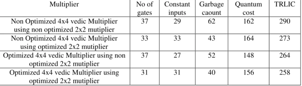
Table 1. Comparison of 4x4 vedic multiplier
Multiplier No of
gates Constant inputs Garbage caount Quantum cost TRLIC Non Optimized 4x4 vedic Multiplier
using non optimized 2x2 mutiplier
37 29 62 162 290
Non Optimized 4x4 vedic Multiplier using optimized 2x2 mutiplier
33 33 43 164 273
Optimized 4x4 vedic Multiplier using non optimized 2x2 mutiplier
37 27 52 148 264
Optimized 4x4 vedic Multiplier using optimized 2x2 mutiplier
31 31 40 156 258
From the comparison Table No.1 we can see that our design requires less number of gates compare to other multipliers. Garbage outputs and quantum cost is also less. Constant inputs required is lesser than four other multipliers. Significant reduction in quantum cost and TRLIC is observed. So, we can say our design is optimized as compare to other designs exist in terms of number of gates, constant inputs, garbage outputs, quantum cost, and TRLIC.
5. SIGNED VEDIC MULTIPLIER
5.1. Algorithm for signed Multiplier
Step1: First we are declaring inputs and outputs.
Step2: Now we are taking MSB bits of both inputs which is a sign bit and now we are calculating XOR of both the bits which indicates sign of the result.
Step 3: Now the negative numbers which are in 2’s complement form should convert to original Form for this we are subtracting the number with 4 in the case of 2x2 and 16 in the case of 4x4 if
at all MSB bit of number is 1.
Step 4: After converting the numbers we are going to call Reversible Unsigned Vedic Multiplier We get the multiplier output.
Step 5 : After getting output from the multiplier we are again converting the number in to 2’s Complement form if and only if output XOR output of MSB’s of input is 1 otherwise We are
taking the direct output.
Signed Vedic Multiplier is used to add signed numbers. Usually in our system negative numbers will be represented in 2’s complement form. So when we are declaring inputs they will be in 2’s complement form. The usage of unsigned vedic multiplier function is good for normal binary form. To use that function we have to convert 2’s complement to normal form and we can call undigned vedic multiplier. The conversion can be made by subtracting the number excluding the sign bit with the corresponding 2n like for 2bit number we have to subtract with 4, for 4bit we have to subtract with 16.
converting the negative number to normal form we are going to call corresponding unsigned multiplier and the result will be in normal form.
Now the output result is converted in to normal form if and only if MSB ouput is 1otherwiswe the output will be taken same . In this signed vedic multiplier the most important step is converting negative numbers in to normal form.
6. RESULTS AND COMPARISON
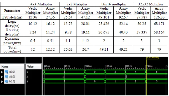
Simulations are carried out using Xilinx 13.1 and synthesized for Spartan3e XS5OO series target board and results are comapared for vedic multilier implemented with normal and reversible gates for the parameters path delay, routing delay and total power(Table No2). The proposed multiplier is also compared with array multiplier for different word sizes as 4bit,8bit, 16 bit and32bit (Table No 3).
Table No. 2 Comparison of 16x16 normal and Reversible vedic multipliers
Parameter Normal Vedic Multiplier Vedic Mutiplier Using Reversible gates
Path delay(ns) 60.23 49.101
Logic delay(ns) 32.12 28.426
Routing delay(ns) 28.11 20.625
Dynamic power(mw) 2.35 2
Total power(mw) 52.21 49.21
From Table No.3 we can say that our proposed multiplier i.e. vedic multiplier is faster than array multiplier.
Table No. 3 Comparison of Varous widths of Vedic and Array Multiplier.
In Fig 8. the simulation result of 2x2 Vedic Multiplier is shown. In this Fig.8 a and b are two inputs of 2bit length and output q of 4bit.
Fig.9 32x32 Vedic Multiplier
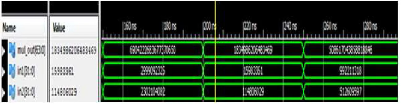
Fig.9 shows the simulation result of 8x8 Vedic Multiplierwhere ‘in1’ and ‘in2’ are two inputs of 32bit length and output taken as mul_out of 64bit.
Fig.10 8x8 signed Vedic Multiplier
Fig 10. shows the simulation result of 8x8 Signed Vedic Multiplierwhere ‘a’ and ‘b’ are two inputs of 4bit length and output taken as ‘h’ of 8bit.
8. CONCLUSION
Vedic mathematics is long been known but has not been implemented in the DSP and ADSP processors employing large number of multiplications in calculating the various transforms like FFTs and control applications such as P, PI, PID Controller implementing in FPGA etc. The proposed Vedic multiplier proves to be highly efficient in terms of speed. Due to its regular and parallel structure it can be realized easily on silicon as well. The main advantage is delay increases slowly as input bits increase. Vedic multiplier can be efficiently adopted in designing Fast Fourier Transforms (FFTs) Filters and other applications of DSP like imaging, software defined radios, wireless communications.
REFERENCES
[1] H. R. Bhagyalakshmi, M. K. Venkatesha, “An Improved Design of a Multiplier using Reversible Logic Gates,” IJEST, Vol. 2, No. 8, 2010
[3] Vijay K Panchal, Vimal H Nayak, “Analysis of multiplier Circuit using Reversible Logic” , International Journal for Innovative Research in Science & Technology.
[4] Prof . Amol D. Morankar, Prof Vivek M.Sakode, “ Reversible Multiplier with Peres Gate and Full Adder”, International Journal of Electronics Communication and Computer Technology, Volume 4,Issue 4,pp-2249-7838, July 2014.
[5] A. Shifana Parween and S. Murugeswari, “ A Design of High Speed, Area Efficient, Low Power Vedic Multiplier using Reversible Logic Gate”, International Journal of Emerging Technology and Advanced Engineering, Volume 4,Issue 2, February 2014.
[6] Krishnaveni D and Umarani, “ VLSI Implementation of Vedic Multiplier with Reduced Delay”, International Journal of Advanced Technology & Engineering Research, Volume 2,Issue 4, July 2012 [7] Swami Bharati Krishna Tirtha, Vedic Mathematics. Delhi: Motilal Banarsidass publishers 1965 [8] Ch. Harish Kumar , “Implementation and Analysis of Power, Area and Delay of Array,
Urdhva,Nikhilam Vedic Multipliers”, International Journal of Scientific and Research Publications, Volume 3, Issue 1,January 2013.
[9] https://www.cs.princeton.edu/courses/archive/fall04/cos576/papers/bennett73.html
[10] R. Landauer, “Irreversibility and Heat Generation in the Computational Process”, IBM Journal of Research and Development, 5, pp. 183-191, 1961.
AUTHORS
Mrs. P. Koti Lakshmi is working as Assistant Professor in the department of ECE at Osmania University , Hyderabad. She has 15 years of teaching experience. She has obtained her AMIETE Degree from IETE, New Delhi in 1999, her M.E in Digital systems in 2004 and persuing Ph.D in VLSI Design from Osmania University , Hyderabad, Andhra Pradesh . Her areas of interest include VLSI Design and Wireless Communications.
B Santhosh Kumar is a student of ME.UCE,OsmaniaUnviversity,Hyderabad. He completed his B Tech from CVR College of Engineering , Hyderabad in the year 2012. His interests are Low power VLSI design circuits, digital circuit designs.
Prof. Rameshwar Rao is the Retired Professor from department of ECE, University college of Engineering,Osmania University,Hyderabad. During his tenure he held many positions as Vice Chancellor of JNTUH, Hyderabad, Andhra Pradesh., Dean, Faculty of Engineering, Osmania University (OU)., Convener, PGECET. He obtained B.E. degree in ECE from OU, M.Tech. and Ph.D. degree from the prestigious IIT Bombay. His work experience spans across 35 years as R&D engineer at Avionics Design Bureau, Hindustan Aeronautics Ltd., Hyderabad and as an eminent teacher at Osmania University,Hyderabad. His reach interests include