Study of Semiconductor Heterostructures
with Embedded Quantum Dots:
Micropillars and Photodetectors
Carlos Alberto Parra Murillo
Study of Semiconductor Heterostructures with
Embedded Quantum Dots
Micropillars and Photodetectors
Carlos Alberto Parra Murillo
Adviser
Prof. Dr. Paulo S´ergio Soares Guimar˜aes
Co-Adviser
Dr. Herbert Vinck Posada
Thesis presented to
UNIVERSIDADE FEDERAL DE MINAS GERAIS
in partial fulfillment of the requirements for the title of
MASTER IN PHYSICS
Instituto de Ciˆencias Exatas
Departamento de F´ısica
Belo Horizonte, Brasil
Agradecimentos
• A meus dois grandes amores, minha m˜ae Maria Pastora e a minha irm˜a Natalia que na distˆancia sempre me apoiam. ´E imensa a saudade e maravilhoso o nosso encontro. Amo vocˆes...!.
• Primeiramente quero agradecer ao professor Paulo S´ergio pela sua orienta¸c˜ao, a amizade, a paciˆencia, o apoio e confian¸ca, e as m´ultiplas discuss˜oes que permitiram desenvolver esta disserta¸c˜ao.
• Ao Professor Herbert Vinck meu co-orientador, pela confian¸ca que depositou em mim quanto vim trabalhar nesse instituto, seus conselhos e discuss˜oes.
• A CAPES e CNPq pela bolsa concedida para a realiza¸c˜ao desse trabalho.
• Ao pessoal do laborat´orio de Semicondutores, Alex, Gustavo, D´eborah, Andreza, Pablo Thiago e Carlitos Pankiewicz pelo ambiente de trabalho, por terem-me ajudado na aprendizagem desta l´ıngua, suas m´ultiplas corre¸c˜oes feitas desde a minha chegada e ao longo da minha estadia aqui no departamento de f´ısica.
• A toda a galera da f´ısica com quem tive a oportunidade de compartilhar momentos muito agrad´aveis e memor´aveis. Por fazer da minha eterna saudade algo f´acil de levar e me fazer sentir mais um deles. Sempre tem um jeito de ser feliz.
• Guilherme Tosi pela amizade e a parceria nessa vida de errante que vou levando nas minhas costas. Leo (Leozim) pelo ˆanimo constante, os conselhos e as risotadas que dei por conta e culpa dele. Na minha terra costumamos dizer:’Gˆenio e figura, at´e a sepultura’. Rodriban pela amizade e a paciˆencia.
Contents
Resumo x
Abstract xii
1 Preliminars 2
1.1 Semiconductor Heterostructures . . . 3
1.2 Optical Microcavities . . . 9
1.3 Infrared Photodetectors . . . 12
2 Pillar Microcavities with Embedded Quantum Dots 17 2.1 Micropillar (DBR Micropost) . . . 17
2.2 Theoretical Modelling . . . 20
2.2.1 Quantum Dot in a Pillar . . . 20
2.2.2 Cavity modes . . . 22
2.2.3 Excitonic-Photonic mode interation in the micropillar . . . 25
2.3 Experimental setup . . . 27
2.4 Results . . . 29
3 Infrared Photodetectors 41 3.1 Description of the Method . . . 41
3.1.1 Introducing Quantum Dots with Different Shapes . . . 47
3.2 Strain and deformation Conduction Band . . . 49
3.2.1 Practical Examples . . . 51
3.3 Some Corrections to the Model . . . 55
3.4 Oscillator Strength . . . 58
Conclusions and perspectives 68
APPENDIX 70
A Numerical Codes Used 71
A.1 CAMFR: Cavity Modeling Framework . . . 71 A.2 Numerical Calculations of Energies and Wavefunctions of Heterostructures 74
List of Figures
1.1 Electronic states for two non-interacting atoms (a), and two interacting atoms (b). Band structure and reduced zone scheme for N interacting atoms (c,d). . . 3 1.2 Occupation of the bands for a metal (a,b), a semiconductor (c), and an
insulator (d). . . 5 1.3 Optical excitations in direct and indirect gap semiconductors. Direct
transition occurs in direct gap semiconductors, whereas in indirect gap semiconductors an additional wavevector K, involving a phonon, is re-quired for a transition with the minimum energy. . . 6 1.4 Schematic drawing of the density of states as function of energy for
three-, and two-three-, one- and zero-dimensional systems in the effective mass ap-proximation. . . 7 1.5 The three types of semiconductor heterojunctions organized by band
alignment. . . 8 1.6 Types of microcavities and their confinement features [44]. . . 11 1.7 Infrared images and applications. . . 14
2.1 Fabrication of a micropillar with embedded quantum dots using EBL and ICPRIE. . . 18 2.2 (Left) Cylindrical micropillar. Image taken by Scanning Electronic
Mi-croscopy. (Right) Schematic process of excitation of excitons by mean of external source. . . 18 2.3 A lens-shaped quantum dot shown with the crystalline axes of the host
material. The double arrow symbolizes the electric dipole that is used in our model to represent the emission. . . 21 2.4 Microphotography of the part of the sample studied, from above, showing
the matrix of micropillars used in the microphotoluminescence experiment. 27 2.5 Microphotoluminescence experimental setup. . . 28 2.6 Photoluminescence spectra for pillar with different diameters. . . 32 2.7 Quantum dot position and orientation effect over modal excitation. Dipoles
2.8 Dependence of the intensity of the fundamental mode emission peak with the radial position of a dot (1,0,0) oriented. . . 34 2.9 Dot dipole position and orientation effect over mode excitation intensity.
Dipole with orientation (0,0,1), located in r = 0.3RP illar (a) and r =
0.6RP illar (b). Radial variation of the T M-mode peak intensity for a
dipole with (0,0,1) orientation. . . 34 2.10 Theoretical spectra for a dipole (1,1,0)-oriented, i.e, a dot dipole with
equal probability of emission in two orthogonal directions in the plane of the cavity and zero probability of an emission perpendicular to this plane. 35 2.11 Comparison of spectra calculated for a dipole (0,1,0)-oriented and a
dipole (1,0,0)-oriented, for r = 0,0.2RP illar,0.4RP illar,0.6RP illar and
0.8RP illar. . . 36
2.12 Experimental spectra for the set of 1.5 µm pillars studied. The spectra are normalized at the fundamental mode. The spectrum shown in (a) is characteristic of the major (70%) part of the samples, with T E01 mode as the most intense of the group of first three excited. In (b), although the T E01 mode is still of higher intensity, theT M01mode is significantly excited, being more intense than HE21. Only one (3%) pillar is in this category. The spectrum (c) is displayed by the remaining 27% of the samples.[Figure from ref. [17]]. . . 38 2.13 Calculated photoluminescence spectra for the 1.5µm diameter
micropil-lars. The PL spectrum in (a) is obtained with a dipole located in the horizontal axis, displaced 0.225 µm (0.3 times the pillar radius) from the center, with polarization in the plane with components X and Y of equal intensities. To obtain spectrum (b), the dipole is located 20◦from the horizontal axis, 0.225µmfrom the center. Its polarization has Y and Z components of equal magnitude and a X component which is 60% of the other two. For spectrum (c), the dipole is located in the horizontal axis, displaced 0.225µm from the center, with polarization in the plane with components X and Y, with the Y component half the magnitude of the X component (See Fig. (2.14)). . . 39 2.14 Flux lines and magnitudes of the Poynting vector of the four lower
en-ergy modes of a circular pillar in the plane of the cavity. The double arrows labeled 1 and 2 represent X-polarized quantum dot dipoles at two different positions in the cavity. . . 40
3.1 Physical system represented by ˆHo, used to construct the basis to expand
the wave functions. . . 43 3.2 Model of the cylinder used to generate the basis of functions for the
problem. . . 45 3.3 An illustration of the process to include the quantum dot potential. . . 46 3.4 Illustrating the process of adding the potential of a few quantum dots
and other layers. . . 47 3.5 (a) Cone-shaped quantum dot (b) cylinder-shaped quantum dot and (c)
3.6 Strained heterostructure scheme showing that the strain propagates in the first atomic planes and along the growth direction. . . 50 3.7 Band offset scheme for InAs quantum dots grown onto InP. . . 52 3.8 Convergence of the method. The dependence of two energy levels, indexed
by the quantum numbers L and K (see text) are shown as a function of basis dimension for different dot shapes:(Black) Circular cylinder, (Blue) circular base cone and (Red) Circular truncated cone. . . 53 3.9 The lowest energy levels and wavefunctions for (a) cylinder, (b) truncated
cone and (c) cone dot shape. . . 54 3.10 (left) GaAs/AlGaAs quantum well energy levels and probability
densi-ties. (right) Effect biaspotential over same system. It is note the shifting of probability densities. . . 55 3.11 Design of a period of the sample (a). Conduction band profile scheme of
the sample (b). . . 60 3.12 Experimental photocurrent spectra. Response peaks are observed in
var-ious energy regions indicating photodetection. . . 60 3.13 Energy levels scheme for sample shown in Fig. (3.11) with a
cylinder-shaped quantum dot of height 7nm and diameter 43nm. . . 62 3.14 Densities of probability (|ψL,K|2) inrz-plane for the wavefunctions
corre-sponding to the most probable optical transitions. Regions correcorre-sponding to different materials are bounded by green lines. . . 63 3.15 Relevant optical transitions in the system, i.e, the transitions with highest
Resumo
Neste trabalho estudamos alguns processos ´opticos em sistemas semicondutores, em
especial, heteroestruturas de dois tipos que contˆem pontos quˆanticos: fotodetectores
de infravermelho e pilares de microcavidades. Os pontos quˆanticos tˆem a fun¸c˜ao de
fornecer el´etrons e/ou quasi-part´ıculas como ´excitons e bi´excitons, fundamentais para
a opera¸c˜ao de dispositivos baseados em pilares de microcavidades e fotodetectores. A
importˆancia dos detectores de infravermelho ´e enorme, com uma imensa variedade de
aplica¸c˜oes, e a relevˆancia das microcavidades tˆem crescido devido `as suas promissoras
aplica¸c˜oes tecnol´ogicas. Apresentamos aqui o estudo te´orico e experimental destas duas
heterostruturas em casos espec´ıficos de nosso interesse. Para investigar o acoplamento
entre os modos fotˆonicos e a emiss˜ao de pontos quˆanticos inseridos em pilares de
mi-crocavidades, foi implementado um c´odigo baseado no software livre CAMFR [Peter
Bienstmann. Cavity modelling framework, http://camfr.sourceforge.net], que
permite-nos modelar dispositivos fotˆonicos como VCSELs e microcavidades. Mostramos que a
partir da an´alise da intensidade de excita¸c˜ao dos v´arios modos dos pilares, ´e poss´ıvel
inferir sobre a polariza¸c˜ao dos pontos quˆanticos neles inseridos. Para auxiliar na
inter-preta¸c˜ao da resposta de fotodetectores de infravermelho baseados em pontos quˆanticos
semicondutores, foi desenvolvido um c´odigo na linguagem de programa¸c˜ao C, o qual
´e baseado na diagonaliza¸c˜ao num´erica da equa¸c˜ao de Schr¨odinger na aproxima¸c˜ao de
massa efetiva, obtendo assim a estrutura de n´ıveis de energia e fun¸c˜oes de onda do
´opticas mais prov´aveis, e entender alguns fenˆomenos interessantes que aparecem no
es-tudo dos detectores de infravermelho. Concluimos que o espalhamento Auger ´e um
Abstract
In this work, we study some of the optical processes that take place into
semicon-ductor systems, specially heterostructures of two types with embedded quantum dots:
infrared photodetectors and microcavity pillars. Quantum dots are the source of
elec-trons and/or quase-particles such as excitons and bi-excitons, which are fundamental
in the operation of devices based on pillar microcavities and photodetectors. The
im-portance of infrared detectors is enormous, with a huge variety of applications, and the
relevance of microcavities have increased due to its promising technological applications.
We present here a theoretical and experimental study of these two heterostructures in
specific cases of our interest. In order to investigate the coupling between the photonic
modes and the emission of quantum dots embedded in microcavity pillars we
imple-mented a code using the free software CAMFR [Peter Bienstmann. Cavity modelling
framework, http://camfr.sourceforge.net], which allows to model photonic devices such
as VCSELs and microcavities. From the analysis of the intensity of excitation of the
modes in the pillars, we showed that it is possible to infer on polarization of the emission
of the embedded quantum dots. Furthermore, to help in the interpretation of the
re-sponse of quantum dot infrared photodetectors, we developed a code on the C-language
which is based in a numerical diagonalization of Schr¨odinger equation for the effective
mass aproximation, in order to obtain the energy levels and wavefunctions of the
sys-tem. The oscillator strengths are computed to quantify which are the most probable
study of infrared photodetectors. We conclude that Auger scattering has a significant
Chapter 1
Preliminars
In this chapter, we present basic physical concepts used in the rest of this text. Concepts
that are important to take into account in order to achieve a better understanding of
the developments, schemes, approximations and statements that will be done mainly
in the two following chapters. We will begin with a brief description of semiconductor
heterostructures in a general framework, and follow describing the two special
semicon-ductor structures which will be studied later.
This dissertation is organized as follows. In the first chapter, we present the basic
fundamentals that will be implemented along this work. A brief introduction about
semiconductor theory is made, and a description of the present situation on
microcav-ities and infrared photodetectors is presented. In the second chapter, we introduce the
microcavity pillar, the theoretical modelling, from a classical point of view, of
pho-tonic excitation process, its efficiency and relation with a polarization of the quantum
dot emission. In the third chapter, it is presented the implementation of the method
introduced by Gangopadhyay and Nag [S. Gangopadhyay e B R Nag. Energy levels
in three-dimensional quantum confinement structures, Nanotechnology, vol. 8, 1997] to
are presented, and an appendix with an introduction to the use of the numerical codes
is made.
1.1
Semiconductor Heterostructures
Before we describe what a semiconductor heterostructure is, we need to define some
concepts from Solid State Physics. This successful branch of physics considers how the
large-scale properties of solid materials result from their atomic-scale properties. The
number of atoms forming a specific material is of the order of 1023, and its properties
are not the same as those of single atoms, as illustred in the figure (1.1), where we see
the split of the energy levels when the inter-atomic distanceRis reduced (a,b). When N
atoms are considered, it is found that there are energy bands (see Fig. 1.1-c) consisting
of N levels, one of each single atom, which form a quasi-continuous because the energy
difference between neighboring levels is negligible (∼10−23eV).
Figure 1.1: Electronic states for two non-interacting atoms (a), and two interacting atoms (b). Band structure and reduced zone scheme for N interacting atoms (c,d).
arranged such that the electron wavefunction in the resulting lattice is given by
φ~k,i(~r) =ei~k·~ru~k,i(~r), (1.1) whereu~k,i(~r) =u~k,i(~r+R~), forR~ being the lattice vector. The solutions (1.1) are known as electron Bloch-functions that solve the Hamiltonian ˆH = ˆH0+ ˆU(~r), with ˆU(~r) the
periodic potential with R~ as period. The Bragg condition allows one to know that just
by considering independent wave vectors in the First Brillouin Zone (FBZ-unit cell in
the reciprocal space) the rest of the band structure is totally determined. Thus, it is
possible to define the so-called reduced zone scheme, in which all ~k’s are transformed
to lie in the FBZ (see Fig. 1.1-d). This scheme is useful, since when the electrons make
a transition from one state to another under the influence of a translationally invariant
operator, k is conserved [30, 3, 49, 29], whereas in the extended zone scheme k is
con-served only to a multiple of 2π/R, however these two schemes are equivalent.
Having obtained the band structure, we want to fill these bands with electrons taking
into account the Fermi-Dirac statistics. Thus, if we assume T = 0 K, there will be
energy bands completely filled and partly filled or empty bands. The uppermost
com-pletely filled band, that is, the completelly filled band with the highest energy, is called
“valence band”(VB), while the partly filled or empty band with lowest energy is called
“conduction band”(CB). The energy region close to the top of the valence band and the
bottom of the conduction band determines not only the optical properties, but also the
magnetic properties and the electronic contributions to the conductivities of electricity
and of heat in semiconductor materials. In this way, the band structure determines
what kind of material we have. If the band with the highest energy which is occupied
by electrons is partly-filled, or if a completely filled band overlaps with an empty or
partly-filled band, we have a metal (see Fig. 1.2-(a,b)). If, on the other hand, the filling
first empty bands, we have a semiconductor (see Fig. 1.2-c) [30] for
0< Eg .4eV, (1.2)
and an insulator for
Eg &4eV. (1.3)
VB VB
VB
VB CB
CB
CB CB
Eg<4 eV Eg>4 eV
space coordinates
energy
(a) (b) (c) (d)
Figure 1.2: Occupation of the bands for a metal (a,b), a semiconductor (c), and an insulator (d).
Depending on size of the gap, the semiconductors are called narrow-gap
semiconduc-tors, for 0< Eg .0.5eV or wide-gap semiconductors, for 2< Eg .4eV. In the range
0.5.Eg .2eV we find the usual semiconductors Ge, GaAs and Si. But this is not the
only one way to classify them, of course. A very important distinction is between the
direct-gap semiconductors, in which the valence band maximum and the conduction
band minimum are located at the same value of wavevector k in the band structure,
usually k = 0, and the indirect-gap semiconductors (see Fig. 1.3), where the minimum
of the CB and the maximum of the VB occur at different k values. Optical transitions
an additional particle such as a phonon in the indirect-gap semiconductors in order to
conserve ~k.
Figure 1.3: Optical excitations in direct and indirect gap semiconductors. Direct tran-sition occurs in direct gap semiconductors, whereas in indirect gap semiconductors an additional wavevector K, involving a phonon, is required for a transition with the min-imum energy.
An important effect in excitation processes such as the ones shown in Fig. (1.3) is the
creation of a particle so-called “hole”in the valence band, which has the properties of
the electron that has been removed from this band, i.e, qh = −qre, ~kh = −~kre, and
spin σh = −σre. Other particle that can be formed in these processes is the so-called
“exciton”which consists of a bound electron-hole pair. The exciton is more correctly
called a quasi-particle since it is a bound state of two particles. Its life time, or
recombi-nation time, is of the order of nanoseconds, and it is usually seen in photoluminescence
measurements. We will show later that this particle can be understood as a classical
dipole for non-magnetic materials where the spin effects are neglected.
In general, the effect of the internal forces on an electron inside a semiconductor material
can be taken into account using the concept of effective mass [29]. Throughout this work,
we use the so-called effective mass approximation [30], where the effective mass depends
1
mef f
= 1
~2
∂2
∂ki∂kj
E(~k), (1.4)
and according to the properties of the band structure, both electron and hole have
positive effective mass, even if the curvature of the valence band is negative [30]. The
Schr¨odinger equation in the effective mass approximation is given by
−~
2
2 ∇
1
m∗(~r)· ∇
ψ(~r) +V(~r)ψ(~r) =Eψ(~r), (1.5)
with m∗ the effective mass, from which we can obtain the band structure of the
mate-rial. There are several method to compute the band structure, some of the most used
are the so-called k ·p method [27] and the tight-binding model [3, 49]. Depending of the complexity of the structure we use the most convenient. Here in this work, we will
solve equation (1.5) by direct diagonalization for structures of our interest.
Figure 1.4: Schematic drawing of the density of states as function of energy for three-, and two-, one- and zero-dimensional systems in the effective mass approximation.
Currently, structures with reduced dimensionality in one, two or three directions, are
The reduction in dimensionality alters the density of states [30], which is given by
CB : D(E) = (E−Eg)d/2−1; E > Eg (1.6)
V B : D(E) =Ed/2−1; E >0; d=dimensionality, (1.7) as shown in the Figure (1.4). The structures for each dimensionality, i.e., for d = 3,
d = 2, d = 1 and d = 0, are usually called Bulk, Quantum Wells, Quantum Wires
and Quantum Dots [30, 49]. Quantum dots are also called quantum boxes, artificial
atoms or nano crystals. They have discrete energy levels due to the three-dimensional
confinement, and have many important potential applications.
Finally, we define a semiconductor heterostructure as a combination of different
semi-conductor materials which are grown one on top of another by using epitaxial
tech-niques such as Molecular Beam Epitaxy (MBE) and Chemical Vapor Deposition [49].
The heterostructure performance depends on the properties of the interface between
the materials involved, the heterojunction, on the effective mass of the two materials,
on their energy gap, strain in the interface, and the band offsets [49, 20, 45, 37, 9].
Three types of heterojunctions, are shown in Figure (1.5).
In our work, all heterojunctions are of type I. The presence of charge, i.e, electrons
or holes, in the material leads to the modulation of the CB(VB) profile, which can be
computed by solution of the Poisson for the electrostatic potential φ(~r)
∇2φ(~r) =−ρ(~r)
ǫǫ0
. (1.8)
whereǫ is the relative dielectric function.
Along this work, we will describe different heterostructures, and all what was exposed
above will help us to understand the results and the interesting phenomenology that
takes place in these structures. In the next section, we describe two types of devices,
microcavities and infra-red photodetectors, which are our structures of interest in this
work.
1.2
Optical Microcavities
The optical microcavity is a structure formed by a region sandwiched between reflecting
faces that allow the confinement of light (photons) with wavelengths well defined, the
so-called modes. These are stationary waves which result from the destructive and
constructive interference caused by multiple reflections in the interfaces between the
material from which the cavity is made and its surrounding materials. The refractive
index contrast between the materials of the cavity, reflecting faces and surrounding, is
relevant because it also helps to improve the confinement, which is quantified by the
quality factor Qdefined as
Q=ω0×
Energy storaged by the cavity
P ower dissipated by the cavity, (1.9)
Q= λ0 ∆λ =
ω0
∆ω, (1.10)
where λ0 (ωo) is the mode wavelength (frequency) and ∆λ (∆ω) is the Full Width
at Half Maximum (FWHM) of the mode spectral lineshape. An important parameter
is the modal volume defined as the effective spatial region where the electromagnetic
mode exists. It is calculated as follows:
V =
RRR
ǫ(~r)|E(~r)|2d3~r
max(ǫ(~r)|E(~r)|2) , (1.11)
with ǫ(~r) the dielectric function. Figure (1.6) shows some types of microcavities with
their corresponding quality factors and modal volumes. The first of these devices, the
micropillar (a) has attracted much attention recently for applications such as
single-photon sources. It offers relative high Q and small modal volume, and the possibility
to incorporate quantum dots as emitters. The Bragg mirrors at the top and bottom
provide one dimension of cavity confinement, whereas air-dielectric guiding provides
the lateral confinement. We will describe and discuss this device in detail in chapter 2.
Y. Yamamoto’s group from Stanford University was one of the first groups that grew
and studied amply the micropillar features [46, 38], and a great quantity of papers have
been published in the last years studying this system and its promising applications.
The structures shown in (b,e) have a special set of modes, which live on the cavity
sur-face, and are called whispering gallery modes. However, these modes are not exclusive
of this type of microcavities. It has been shown that by lateral excitation of micropillars
these modes can form part of the set of modes for these structures [4]. The whispering
modes are similarly excited in microspheres, microtoroids and microdisks, by coupling
from a fiber-taper waveguide and subsequently guided within and along the periphery
mi-cropillar quality factors.
Figure 1.6: Types of microcavities and their confinement features [44].
The atom trap is other type of microcavity, in which the atomic centre of mass motion
for ultracold atoms, i.e., atoms with thermal energy smaller than the coupling energy
~Ω in a strongly coupled system, is altered by interaction with the vacuum cavity
mode, which is similar to the Fabry-Perot resonator (see Fig. 1.6-d). Ω is the Rabbi
coupling frequency. The atom inside the trap (cavity) entrains in an orbital motion
before scaping, thus, because the coupling energy depends on the amplitude of the
vac-uum cavity field near the atom, optical transmission probing of the cavity during the
atomic entrainment acts as an ultrasensitive measure of atomic location [23, 21]. The
most recently studied microcavities are those embedded into a photonic crystal (see
fig. 1.6-c), in which they are treated as the defect in the crystal or they can be part of
the well-known unit cell of the crystal [25, 13]. This type of device is a very important
research topic nowadays and there are many groups working in its fabrication
improve-ment. The quality factor of photonic crystal cavities, theoretically speaking, has been
predicted to be of the order of 103 −105 [2]. As in micropillars, in photonic crystals microcavities the growth of quantum dots inside the cavity is easily accomplished. The
that determine the efficiency of modal excitation in the cavity [17], for this reason, the
growth of quantum dots precisely located has been studied, in order to create structures
of high performance [36].
Even thoughQ and V are the most relevant microcavities parameters, there are
alter-native measures of performance for these structures, for example, the cavity finesse
[44, 10, 16], which does not include the propagation effects as does the Q factor.
All these microcavities properties exposed above make these systems excellent
candi-dates to recent and future applications in optical telecomunications, quantum optics,
and diverse areas that involve optical devices.
1.3
Infrared Photodetectors
The mid-infrared photodetectors are another kind of semiconductor structure usually
based in semiconductors made of elements III and V of the periodic table. The research
and development in this area comes from the need to fabricate opto-electronics devices
that have many applications in, e.g, telecommunications, aerospace and defense. The
particular application determines the infrared region for which we need to design the
device. In general, only a specific region of the spectrum is of interest and sensors are
designed to collect radiation only within a specific bandwidth, although broadband
detectors are also of some interest. The infrared region is subdivided in various regions:
• Near-Infrared (wavelength from ∼ 0.5 µm to ∼ 1.4 µm): used for fiber optic telecommunication and night vision.
• Short-Wavelength Infrared (λfrom∼1.4µmto∼3µm): in this region the water absorption increases significantly, but it is also good for long-distance
• Mid-Infrared (λ from ∼3µm to∼8µm): interesting region for defense applica-tions, as guided missile technology of 3−5µm.
• Long-Wavelength Infrared (λ from ∼ 8 µm to ∼ 15 µm): this is the “thermal imaging”region, in which sensors can obtain a completely passive picture of the
outside world based on thermal emissions only and requiring no external light or
thermal source such as the sun, moon or infrared illuminator. Sometimes is called
far-infrared region.
Presently, the state-of-the-art detectors are quantum well infrared photodetectors (QWIP)
[32], indium antimonide (InSb) detectors, and mercury-cadmium-telluride detectors
(HgCdTe), however several different authors have proposed a new kind of detectors,
the quantum dot infrared photodetectors (QDIP), which have some advantages over
the infrared radiation detectors mentioned above. We can say the QDIPs are part of
the third-generation of infrared detectors [41]. The QDIP is similar to the QWIP, in
the sense that both are based in the intersubband level transition in either conduction
band or the valence band in the heterostructure designed to work in a specific
wave-length. The main differences between these devices are, first the QDIP allows normal
incidence, this is, the incident light normal to the wafer along the growth direction is
expected to cause transitions, which greatly simplifies the fabrication process. Second,
a significant reduction of the dark current is obtained, which makes it possible to
op-erate the detector at temperatures higher than a QWIP. Recently, tunneling structures
that combine quantum dots with quantum wells and with potential barriers have been
proposed in order to obtain more selective detectors and also to reduce the dark current
[41]. This kind of multilayered structures promises the future development of infrared
photodetectors that operate at moderately low temperatures or even at room
Figure 1.7: Infrared images and applications.
So far, we made a brief review of infrared photodetectors, now we define the main
physical features that need to be studied and optimized, in order to understand the
performance of these devices. We begin with the dark current, which can be estimated
by counting the mobile charge density thermally excited and multiplying by the carrier
velocity as follows
hjdarki=evn3D, (1.12)
wherev is the drift velocity andn3D the density of thermally excited carriers, which is
given by
n3D = 2
mbkBT
2π~2
3/2
exp
− Ea KBT
, (1.13)
where mb is the effective mass of the region where the dark current is calculated, and
Ea is the thermal activation energy, which is equal to the difference between the Fermi
energy and the first continuum level in the structure. This current is the major cause of
noise in the detection and depends strongly on the temperature, becoming 2A/cm2 for
temperatures near 300K [5]. Obviously, that is an effect that needs to be reduced, and
that is possible by use of a QDIP structure combined with potential wells and barriers,
follows
hjphotoi=eσIhni, (1.14)
where σ is the cross section of the electron excitation, I is the radiation intensity and
n the density of electrons optically excited. In this way, we can define the so-called
responsivity R of the device as
R = ∆j
e~ωI = e
hνηg, (1.15)
with ∆j =jphoto−jdark,ηdefined as the absorption efficiency andgthe photoconductive
gain
g = τlif e
τtrans
, (1.16)
whereτtrans is the transit time across the device, andτlif e is the lifetime of the
photoex-cited electron. The figure of merit used to evaluate the performance of most QWIPs
and QDIPs is the specific detectivity (D∗), which is a measure of signal-to-noise ratio and it is given by
D∗ = R
√ Af p
4hjdarkigdevice∆f
, (1.17)
here, A is the device area, f is the measurement frequency, ∆f (= 1 Hz) is the
bandwith frequency, gdevice is the photoconductive gain of the device, which, in the case
of a QDIP, is given by
g = (1−Pc) (MF Pc)
, (1.18)
wherePc is the capture probability, and F is the fill factor [34]. The features mentioned
Chapter 2
Pillar Microcavities with Embedded
Quantum Dots
In this chapter, we present a detailed explanation about the exciton-photonic modes
interaction in pillar microcavities in order to understand how this can be made more
efficient and also to explain the surprising experimental results obtained and the
inter-esting consequences of these results. We begin by introducing the characteristics of the
system and the modelling made. The work reported here was published in the article:
Optics Express Vol. 16, No 23, pag.19201, (2008).
2.1
Micropillar (DBR Micropost)
The pillar microcavity is usually fabricated from a semiconductor heterostructure grown
by Molecular Beam Epitaxy (MBE) which consists in aλ-thick GaAs microcavity with
lower and upper Bragg mirrors composed of, respectively, N1 and N2 periods, each one
consisting of (λ/4)-thick GaAs and AlxGa1−xAs layers with refractive indexes nGaAs
and nAlGaAs. Here λmust be understood as the wavelength of radiation in the material.
In the middle of a cavity a InAs layer is grown to create self-assembled quantum dots by
are fundamental for this kind of studies. It is known that the geometry of the pillar
determines what kind of photonic modes can be supported by the cavity, for instance, if
the cavity is planar, the family of modes is{T E, T M}and there is no mixture between them as in the case of circular and elliptical pillars; in our work the micropillars studied
have cylindrical geometry and were fabricated by Electron Beam Lithography (EBL)
and Inductively Coupled Plasma Reactive Ion Etching (ICPRIE) (see Fig. 2.1) [12].
Figure 2.1: Fabrication of a micropillar with embedded quantum dots using EBL and ICPRIE.
As result of this process we have the pillar shown in the Scanning Eletronic Microscopy
technique image of Figure (2.2). But, why is it important to design this system with
all these specific characteristics? The first interesting property of this system is the
confinement of photons in the microcavity due to two relevant processes: (a) contrast
between refractive indexes, in our case 3.510 to 2.497 for the cavity and the materials up
and down this respectively. Laterally there is air, so the contrast is large, 3.510 to 1.0.
These contrasts allow that by total internal reflection (TIR) a wave can propagate along
a particular direction as in the case of a waveguide. (b) The second important process
is the multiple reflections in the interfaces between the materials in the Bragg mirrors
which, by constructive and destructive interference, stationary waves, also calledmodes,
are created in the cavity. The lifetime of the cavity modes can be increased by increasing
the number of the Bragg reflectors, because these damp the outgoing radiation thus
increasing the confinement due to its high reflectivity, and therefore making light storage
possible. The most interesting phenomenon that is observed in this system is the
so-called Purcell effect [40] which establishes that the radiation properties of an atom
can be modified controlling the boundary conditions of the electromagnetic field with
mirrors or cavities. The existence of this effect means that it is possible to enhance
the spontaneous emission rate, also called incoherent radiation, and store just coherent
radiation in the cavity. In other words, let Γ0 and Γ be the spontaneous emission rate of
an atom that is located inside and outside of the cavity, respectively. The Purcell factor
(F) is defined as the ratio between these two emission at the resonance wavelength λ
rates. It is possible to show [46] that for any atom-field coupling regime it is given by
F = Γ Γo ∼
3Qλ3
4π2V , (2.1)
whereQis the quality factor of the cavity, λis the frequency of the mode andV is the
Let us note here that F depends on the ratio Q/V, which must be optimized by
in-creasing Q and decreasing the modal volume V, but these parameters in general vary
in opposite ways. For example, a decrease in the pillar size, in order to obtain a small
V, will lead to lower Q, due to problems of fabrication and surface losses. Therefore,
a compromise between these parameters has to be found. For the strong atom-field
coupling phenomenon the parameter to maximize is Q/√V [28, 47].
These interesting properties make the micropillar system a good option for multiple
technological applications [44]. For example, a micropillar with embedded quantum
dots is a very good single-photon source. This system is equally interesting for
fun-damental physics studies because some basic principles and phenomena such as
quan-tum interference can be investigated using these devices as sources in, for instance, a
Hanbury-Brown-Twiss setup, a Mach-Zehnder interferometer and others.
2.2
Theoretical Modelling
So far, we presented the physical characteristics of our system and how to improve these
in order to get the best performance of the devices. Now we show the theoretical model
which we implemented to describe the interesting experimental results of
microphotolu-minescence measurements of an array of nominally identical GaAs/AlGaAs pillars with
embedded quantum dots.
2.2.1
Quantum Dot in a Pillar
Let us consider a quantum dot modelled as a permanent electric dipole ~p =q ~d, which
has six degrees of freedom that determine its position and orientation (polarisation).
As a result of the growth process the dot z-position is fixed in the middle of the
use of the r and φ coordinates. For the dot orientation (polarisation), we need three
coordinates, which will be the cylindrical coordinates (r′, φ′, z′). In the figure (2.3) we
show a quantum dot with lens shape [14], and its schematic dipole, that we will use to
represent its photon emission. The growth directon is along the [001] crystalline axis of
the host material.
Figure 2.3: A lens-shaped quantum dot shown with the crystalline axes of the host material. The double arrow symbolizes the electric dipole that is used in our model to represent the emission.
Both the position and orientation of emission of the quantum dot are not controllable
parameters in the growth process. It has been shown experimentally and theoretically
that when an exciton is created in an InAs/GaAs quantum dot, spatial separation of
the electron and the hole may create an oriented dipole. However, this result is not clear
since some autors [14] have obtained results which indicate that the electrons are at the
bottom of the dot and the holes are located above them, which is exactly the opposite
of what band theory predicts [20, 39]. Currently there is not a definitive solution for
this controversy, which is probably due to the fact that the dot shape is very relevant.
If the dots have azimuthal symmetry around the [001] growth axis, the fundamental
excitonic transition is unpolarized as observed in most experimental studies. However,
the InAs/GaAs quantum dot is in general asymmetric in shape and composition and
quantum dots: emission orthogonally polarised along the [1¯10] and [110] crystalline
directions have been reported by several authors [15, 31]. Polarization along the [001]
growth direction is also seen, although more rarely and mostly for special situations
[24, 43]. In this work we present results which show how relevant both position and
orientation of the quantum dots are in order to understand some differences in the
photoluminescence spectra obtained.
2.2.2
Cavity modes
Principles of classical electromagnetism can be used to study micropillars and similar
kinds of photonic systems due to size scale of the structures. The Finite
Difference-Time Domain (FDTD) method is one of the techniques frequently used because of the
reliability of the results. Some softwares use optimized algoritms allowing their
imple-mentation to study complex structure. Among these we mentionMPB[26], FullWave
[1] and CAMFR[8]. The last one is the tool used by us in this work. In the following we present briefly the physical basis of this software and how we modelated the physical
system and the cavity modes.
To understand howCAMFRworks, first we describe the method so-calledeigenmodes expansion [6], which works in the following way:
(i) We begin with Maxwell equations with no sources, which are
∇ ·D~ = 0 (2.2a)
∇ ·B~ = 0 (2.2b)
∇ ×E~ =−∂ ~B
∂t (2.2c)
∇ ·H~ = ∂ ~D
These equations can be decoupled using the vectorial identity ∇ ×(∇ ×A~) = (∇ ·A~)∇ − ∇2A~. Combining the Amp´ere law and the Faraday induction law we obtain the wave equations for each field
1
µǫ(~r)∇
2E~(~r) =ω
c
2
~
E(~r) (2.3)
∇ ×
∇ × 1
µǫ(~r)H~(~r)
=ω
c
2
~
H(~r) (2.4)
for which harmonic solutions are normally proposed, as follows
~ E(~r, t)
~ B(~r, t)
=e
−iωt
~ E(~r)
~ B(~r)
. (2.5)
(ii) Consider a structure that consists of different materials with refractive indexes
ni’s. This structure is divided in regions where the refractive index is constant,
and the spatial part of the solutions of (2.5) are found for each region, forming a
set of eigenmodes{Ek, Hk}, in which the general solution is expanded as follows,
~
E(~r) =X
k
AkEk(~r)
~
H(~r) =X
k
AkHk(~r).
(iii) With each solution totally established, it is necesary to find the fields for the
structure by coupling the adjacent regions. For this, there are two schemes:
electromagnetic fields in the interfaces between each two materials [48]. With this
method, that does not depend on the sources, it is possible to calculate either the
reflection or transmission spectra. From them is possible to get the energy modes
and calculate their quality factor.
S-Scheme: In this, the outward-propagating fields of the structure (non-guided or leaky modes) are related with the inward-propagating fields ((non-guided
modes), which allows to study the dissipation in the system by means of the
quality factorQ.
The process is applicable for any structure, and the calculation times depend on the
ge-ometry. CAMFR has an additional feature, the Perfect Matched Layer method (PML)
[7]. This method allows to absorb the unbounded modes at the simulation window
boundary in order to eliminate the parasitic reflections.
In the present case, we use cylindrical coordinates for which the transformation
equa-tions are given by
x=r cosθ
y =r sinθ
z =z
The wave equations for thez-components of the fields are as follows
∂2
∂ρ2 + 1 ρ ∂ ∂ρ + 1 ρ2 ∂2
∂θ2 +
∂2
∂z2 +k 2
−β2
Ez(~r)
Bz(~r)
= 0. (2.6)
(AJl(ktρ) +BNl(ktρ)) (Ccos(βz) +Dsin(βz))eilφ, (2.7)
wherekt=
p
k2−β2, with βbeing the effective vector along the propagation direction
z. The other components can be obtained from these, because, by manipulation of the
equations (2.2) it is easy to write them in terms of Ez and Hz. For the set of
solu-tions (eigenmodes) to be complete it is necessary to determine the constants, A, B, C
and D, which is done by use of the boundary and orthonormalization conditions. The
fields are labeled using the conventional notation for waveguide modes, i.e., there are
two families of solutions, HE and EH, the so-called hybrid modes. They are defined
depending on the ratio Ez/Hz, in this way, if this ratio is greater than 1, we have EH
modes and if the ratio less than 1, the modes are HE. In these families, there are two
particular sets of pure modes. The first of these occurs when the ratioEz/Hz tends to
zero, this means that justHz is projected along the z direction. These modes are called
tranverse electric (T E). The other situation is when the ratio Ez/Hz tends to infinity,
so the component projected ontozisEzand the modes called tranverse magnetic (T M).
Inward and outward-modes of the structure are found expanding in this basis and
will be totally determined by use of either the T-Scheme or S-scheme, and so other
optical properties can be computed with the CAMFR code. In the next sections, we
bring everything together and focus our attention in the study of a quantum dot-dipole
interacting with the photonic modes in a micropillar.
2.2.3
Excitonic-Photonic mode interation in the micropillar
The interaction between quantum dot-dipole and a cavity mode from a classical point
Uint=−~p·E~lmn(~r), (2.8)
from which some important details become apparent:
(a) The coupling is maximized for E~lmn parallel to ~p, which could be controlled by
changing the dot orientation, but this is at the least difficult to do in practice.
In addition, the field lines are not uniformly distributed and therefore the ideal
orientation depends on the spatial location of the dot.
(b) The spatial distribution of the field in the cavity also affects this interaction, because
the field has variable magnitude in this and it is zero in some regions [33], due to the
pattern of stationary waves created. So, the position of the dot is also an important
parameter and could be changed in order to optimize the coupling.
(c) It is clear then that the location of the dot and the polarization of its emission
are very important in order to obtain a strong coupling with the electromagnetic
modes. The development of techniques to grow quantum dots in specific positions,
for example, where the field is maximum in order to improve the coupling, has been
a lively investigation topic.
The great difficulty from the experimental point of view is that parameters such as dot
shape, dot charge distribution and, therefore dipole orientation and position of the dot
are random in the fabrication process. In this way, there is no certainty which one of
the dots is better coupled with the field, and which are its characteristics. Recently,
some [36] works showed progresses in the fabrication of heterostructures with quantum
2.3
Experimental setup
The samples studied in this work were grown by MBE in the Sheffield University, UK,
and the experimental measurements were made by Dr Andreza G. Silva and PhD student Pablo T. Valentimfrom Universidade Federal de Minas Gerais, Brasil. The density of InAs-dots in the cavity is of the order of 1010cm−2 and it was estimated that
a number between 20 and 100 dots were randomly located in the central cavity plane.
The distributed Bragg reflectors consist of Nlower = 27 and Nupper = 20 pairs of GaAs
and Al0.8Ga0.2As, each one with thickness 69.3nm and 78.0nm respectively.
Figure 2.4: Microphotography of the part of the sample studied, from above, showing the matrix of micropillars used in the microphotoluminescence experiment.
In Figure (2.4) it is possible to see the 8×8 matrix of micropillars, from which were chosen 33 nominally identical pillars with circular cross sections of 1.5µm of diameter.
This selection was made choosing those pillars on which neither its fundamental nor the
three first excited modes showed a splitting, which would be an indicative of deviations
from circular symmetry. The fundamental mode shows afull width at half maximumof
Figure 2.5: Microphotoluminescence experimental setup.
with wavelength in this range are selected. In Figure (2.5) we present the
microphoto-luminescence setup used, where the excitation is provided by a titanium-sapphire laser
tuned at 740 nm. A microscope objective with numerical aperture of 0.4 is used to
focus the excitation beam to a spot with diameter ≤ 2µm.
The emission from the micropillar was collected by the same objective, focused on
a 0.75 m monocrhomator, and detected by a nitrogen cooled charge-coupled device
detector. All these measurements were made with a resolution of 0.05nm and at T =
2.4
Results
In order to complement the theoretical modelling, we explain here the principal
com-mands used to compute the desired spectrum of the system. CAMFR code is based in
the Python interpreter, which contains a variety of libraries that can be called by a
simple python script. For example, before the pillar and its characteristics are defined,
the libraries need to be imported as follows
from camfr import *
The comments in the code start with #. By means of the following sequence it is
pos-sible to design the structure, First we use the routine Stack to define both top and
bottom of the pillar. Its argument consists of the half to the cavity plus the N Bragg
reflectors, as follows
# Defining pillar top
top = Stack(2*capa GaAs(d GaAs)+N capas der*(capa AlGaAs(d AlGaAs)+
capa GaAs(d GaAs))+space(0))
# Defining pillar bottom
bottom = Stack(2*capa GaAs(d GaAs)+N capas izq*(capa AlGaAs(d AlGaAs)+
capa GaAs(d GaAs))+space(0))
# Cavity
cavity = Cavity(top,bottom)
where the routine Cavity connects these two parts. Each layer is defined using the
routine Circ (Slab in rectangular coordinates) in the following way
capa AlGaAs = Circ(AlGaAs n(r core)+air n(work space−r core))
withr corethe pillar radius. Therefore, so we have a layer that consists of two
concen-tric circular cylinders, with the inner one being the circular pillar layer. The space
between the cylinders, which has a width work space−r core, contains air. Here,
work space is the lateral size of the simulation window. As we said before (see Sec.
2.2.2), the radiation that reaches the boundary of the simulation window is absorbed for
this by use of PML condition. That boundary is located in the wall of the outer cilynder.
The dipole parameters are also simple to introduce by the routineCavity.set source,
as follows
cavidad.set source(source pos,source orientacion)
and both position and orientation of the dipole are controlled by the routine Coord
source pos = Coord(r, φ, z)
souuce orientacion = Coord(r′, φ′, z′)
We must take into account that the dipole orientation does not match in all cases with
the polarization of the dot emission. For instance, if we have a dipole (1,0,0)-oriented,
this orientation is equivalent to a dot emission [110]-polarized, but if the dipole is
(0,1,0)-oriented, we can not infer the polarization of the dot emission, i.e., it is
unpo-larized. However, it is possible to write the polarization states of the dot emission in
terms of the pure dipole orientations here defined.
With the structure defined, we compute the power flux along the z-direction between
power flux = top.ext S flux(r0,r1,relative error)
which allows us to compute the photoluminescence spectra (λ,power flux) and study
the variations that these suffer as the pillar and dot parameters are changed. For
in-stance, it is possible to get a good fit of the experimental spectra modifying the refractive
indexes of the materials involved respectively. The refractive indexes values for GaAs
and Al0.3Ga0.7As are 3.5 and 3.0, respectively. However, the actual values depend on the physical conditions of the experiment such as temperature, which, by creation of
phonons in the crystalline lattice modify the dielectric function of the material, and
therefore the refractive index. The following approximation is reported in the literature
to compute the dependence of the refractive index on the temperature:
n(T) =n0−10−5(T −T0)
.
The refractive index also depends on the wavelength and on the Al concentration for
AlxGa1−xAs and it is difficult to determine a priori the exact value of the refractive
in-dexes that should be used. We use the values reported in the literature and do the fine
adjustment by fitting the fundamental mode position of a set of experimental spectra
of micropillars of different diameters, such as the spectra shown in Figure (2.6).
We obtain a good fit of the energy of the peaks in experimental spectra such as those
of the figure (2.6). We also note that the shifts in the energies of the peaks with pillar
diameter are in good agreement with the tendence reported by Gerard et al. [19], where,
for the case of the fundamental mode HE11, its energy decreases up to a saturation
value as the pillar diameter increases. Similar behavior is observed for the quality
Figure 2.6: Photoluminescence spectra for pillar with different diameters.
microcavity, i.e., the Qvalue of the microcavity sample as grown, before fabrication ot
the pillars. Another important observation here, is that as the diameter of the pillar
is increased, the energy separation between the first three excited photonic modes
de-creases, and they tend to be near the fundamental mode energy. Before showing the
results of this study, we present some interesting situations that help us to understand
the optical properties of our system.
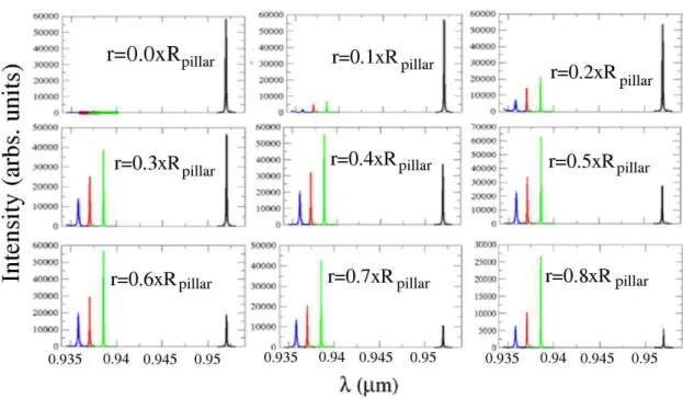
Figure (2.7) shows the theoretical spectra obtained for different dot parameters. We
see that some photonic modes are not excited for some dot orientations and positions,
for example, the T E mode is the only one excited for a dot (0,1,0)-oriented but its
intensity is reduced as the dot is near to the center of the cavity. For these low energy
spectra, the fundamental mode is the one mostly excited, but we see that its intensity is
Figure 2.7: Quantum dot position and orientation effect over modal excitation. Dipoles with orientations (1,0,0), (0,1,0), (1,1,0) and (1,1,1), located in r = 0.3RP illar and
r = 0.6RP illar, where Rpillar is the radius of the pillar.
of the dot in the intensity of the fundamental mode is shown in the figure (2.8) for
angular position φ= 0.
A different behavior is seen in Figure (2.9), where we note that the T M mode is the
only one excited for a dot (0,0,1)-oriented, and that its peak intensity varies as the
radial dot position changes. The intensity of excitation is relatively small compared
with the high excitation intensity of the modes for a dot (1,1,0)-oriented, as seen in
the spectra of Figure (2.10), in which it can be noted that the relative intensity of the
three first excited modes is approximaterly constant as the dot radial position changes.
For r= 0 these modes are not excited.
Figure 2.8: Dependence of the intensity of the fundamental mode emission peak with the radial position of a dot (1,0,0) oriented.
Figure 2.9: Dot dipole position and orientation effect over mode excitation intensity. Dipole with orientation (0,0,1), located in r = 0.3RP illar (a) and r = 0.6RP illar (b).
Radial variation of the T M-mode peak intensity for a dipole with (0,0,1) orientation.
excited modes of lowest energy change with dot position and orientation inside the
pillar. Figure (2.10) shows spectra for these modes and also the fundamental mode
calculated for excitation by a dipole which is oriented in the plane of the cavity, for
several radial positions inside the pillar. It is clear from the figure that the intensity of
excitation varies significantly with dipole (dot) position. The effect of the orientation
spectra for the four modes of lowest energy for two orientations of the dipole in the
plane of the cavity Silva. et al. [17] investigated the emission of 33 nominally identical
pillars with circular cross sections of 1.5µmdiameter. The fundamental mode in these
samples shows an experimental full width at half maximum of (0.22±0.05)nm, which corresponds to aQ around 4300. The 33 pillars investigated were selected from a set of
62 as those in which neither the fundamental nor the first three excited modes showed
a splitting, which would be an indicative of deviations from circular symmetry. We
also chose only pillars which had the fundamental mode emission wavelength inside a
0.22 nm range. We therefore can be reasonably sure of the circularity and regularity
of our pillars, an assumption that was subsequently confirmed by scanning electron
microscope images of some of the samples.
Figure 2.10: Theoretical spectra for a dipole (1,1,0)-oriented, i.e, a dot dipole with equal probability of emission in two orthogonal directions in the plane of the cavity and zero probability of an emission perpendicular to this plane.
Figure 2.11: Comparison of spectra calculated for a dipole (0,1,0)-oriented and a dipole (1,0,0)-oriented, forr = 0,0.2RP illar,0.4RP illar,0.6RP illar and 0.8RP illar.
of the 1.5 µm pillars. For all pillars, the fundamental HE11 mode is always the most
intense but there is a clear distinction in the spectra concerning the relative intensities
of the three higher energy modes. Of the 33 pillars investigated, 70% showed spectra
similar to the one shown in Fig. (2.12-(a)), with the T E01 mode more intense than the
HE21 while the T M01 is weaker. TheT M01 mode is seen with relatively high intensity
in only one sample (3%), shown in Fig. (2.12-(b)). The remaining 27% of the pillars
showed spectra such as the one displayed in Fig. (2.12-(c)), with theHE21 as the most
intense mode of the group of three excited modes.
The experimental spectra shown in Fig. (2.12) were reproduced using the CAMFR code
(see Fig. 2.13) establishing the following conditions for the dot dipole:
Spectrum (a): Equal probabilities of excitonic dot emission in the X and Y directions,
which can be identified with the [110] and [1¯10] crystalline directions.
These directions are in the cavity plane perpendicular to the growth
are intense enough and the coupling is good. But this is not the only
way to reproduce this spectrum, e.g, if the dot is polarized along the X
direction and is located in other position we can obtain the same result.
This result can be better understood with reference to Fig. (2.13), which
shows schematically the electric field profiles for the four lowest energy
modes relative to the dipole, for two polarizations of the dipole in the
plane (1,1,0).
Spectrum (b): This spectrum is a little complicated to reproduce due to the relative
intensity of modes T M01 and HE21. Only if the z component of the
dot polarization is relevant enough the relative intensities shown in the
experimental spectrum can be reproduced. This means that it is not
possible to have T M01 more intense than HE21 without a considerable
degree of Z-polarization. The theoretical spectra shown in Fig. (2.13-(b))
was obtained with polarization Y/Z=1 and X=60%Y.
Spectrum (c): In this case the relation between the components of the dot polarization
taken was X=2Y and the dot is located in position 2 of Figure (2.13). The
same kind of spectrum is obtained for a dot predominantly Y-polarized
but located in position 1 or Figure (2.13).
All results discussed above imply that a large part of the quantum dots inside the pillar
are polarized. This conclusion was verified from photoluminescence measurements at
low power excitation, ∼1 µW [11], which showed experimentally that in a pillar that has a spectrum such as that shown in Figure (2.13)-(c) several dots are linearly
polar-ized. The polarization is usually found to be along [1¯10] with a degree of polarization
as high as 90%. In the case of spectum (2.13)-(b), determining if there are dots with
z-polarisation well defined is difficult, since it would require lateral detection of the
Figure 2.12: Experimental spectra for the set of 1.5 µm pillars studied. The spectra are normalized at the fundamental mode. The spectrum shown in (a) is characteristic of the major (70%) part of the samples, with T E01 mode as the most intense of the group of first three excited. In (b), although the T E01 mode is still of higher intensity, the T M01 mode is significantly excited, being more intense than HE21. Only one (3%) pillar is in this category. The spectrum (c) is displayed by the remaining 27% of the samples.[Figure from ref. [17]].
of Z-polarization of the emission for the dots in these pillars. In conclusion, we showed
that the relative intensities of the electromagnetic modes can be used to obtain
infor-mation about the polarization of emission of quantum dots embedded in micropillars.
Summarizing all aspects treated in this chapter, by means of a relatively simple
the-oretical modelling we were able to understand some interesting results obtained for
circular micropillars. These are structures which have been studied by many different
groups in the world over the last years due to their several potential applications. We
verify experimentally that the efficiency of excitation of the various photonic modes
of the microcavity pillar depends significantly on the position and orientation of the
Figure 2.13: Calculated photoluminescence spectra for the 1.5µm diameter micropillars. The PL spectrum in (a) is obtained with a dipole located in the horizontal axis, displaced 0.225 µm (0.3 times the pillar radius) from the center, with polarization in the plane with components X and Y of equal intensities. To obtain spectrum (b), the dipole is located 20◦from the horizontal axis, 0.225 µm from the center. Its polarization has Y and Z components of equal magnitude and a X component which is 60% of the other two. For spectrum (c), the dipole is located in the horizontal axis, displaced 0.225 µm
from the center, with polarization in the plane with components X and Y, with the Y component half the magnitude of the X component (See Fig. (2.14)).
was also showed that a large percentage of the dots in our pillar have a considerable
degree of linear polarization, which has been experimentally confirmed. The analysis
of the relative intensity of the photonic modes allows us to estimate the overall degree
of in-plane polarization of the quantum dot ensemble and also to give information on
HE
11TE
01HE
21TM
01Chapter 3
Infrared Photodetectors
In this chapter, we present the basic ideas of the method proposed by Gangopadhyay
and Nag [18] to calculate the energy levels of semiconductor structures with quantized
momentum in one or more directions, as in the case of quantum wells, wires and dots,
and more complex heterostructures used by specific technological applications such
as photodetectors devices. Then we describe the implementation of this method to
calculate the structures of our interest, namely, quantum dot infrared photodetectors,
and describe the results obtained for a particular structure.
3.1
Description of the Method
In order to calculate the energy levels of this kind of system, we use the Schr¨odinger
equation in the effective mass approximation with dimensionless units, given by:
−
∇mm∗(e~r) · ∇
ψ(~r) +V(~r)ψ(~r) =Eψ(~r), (3.1)
withmethe free-electron mass and m∗(~r) is the effective-electron mass in structure. We
adopt the RydbergRy = 13.6eV as the unit of energy and the Bohr radiusao = 0.529 ˚A
by Ry and the lengths by ao to get the real value.
To solve (3.1),ψ(~r) is expanded in a suitable set of functions which are solutions of a
similar but less complex system. In other words, let ˆH be a Hamiltonian operator of
our system which can be separated as follows
ˆ
H= ˆHo+ ˆV (3.2)
where ˆV represents the potential of the system and ˆHo is the Hamiltonian of a simple
problem which satisfies the eigenvalue problem
ˆ
Ho|gii=Ei|gii,
with{gi}being the set of functions in which any general functionψ(~r) will be expanded,
ψ(~r) =X
i
aigi(~r), (3.3)
for gi(~r) = h~r|gii. We choose the system represented by ˆHo to be an electron with
effective mass me confined in a large cylinder of potential Vo = 0, radiusR and height
L which is surrounded by air as it is shown in Figure (3.1).
To find {gi} we must solve the Schr¨odinger equation in cylindrical coordinates by
sep-aration of variables
gi→l,m,n(r, ϕ, z) =Rlm(r)φl(ϕ)Zn(z) (3.4)
Figure 3.1: Physical system represented by ˆHo, used to construct the basis to expand
the wave functions.
d2
dϕ2φl+l 2φ
l = 0
d2
dz2Zn+ k 2
−l2
Zn = 0 (3.5a)
ρ2 d
2
dρ2Rlm+ρ
d
dρRlm+ ρ
2
−α2
Rlm = 0
whereρ=αr and k2 = 2m
eE/~2. By use of boundary conditions glmn(r=R, φ, z) = 0
and glmn(r, φ, z = 0, L) = 0, we have
Rlm(r) =
√
2
RJl+1(klm)
Jl klm r R , (3.6)
Φl(ϕ) =
1
√
2πe
Zn(z) = r 2 Lsin nπ L z . (3.8)
with the orthonormalization condition given by
Z
V
dV gl∗′m′n′glmn =δl′lδm′mδn′n. (3.9)
The energies levels for this problem are
Elmn =
~2
2me
n2π2
L2 +
k2
lm
R2
,
with klm the m-zero of the Bessel function of order l. With this set established, we
are going to study the problem of a quantum dot embedded in a cylinder like the one
described above. For this, we need to solve the eigenvalue equation
ˆ
H|ψi=E|ψi,
where ˆH contains all information about the quantum dot and barriers (mass and
po-tential). So, if we replace equation (3.3) into (3.1), multiply this byg∗
l′m′n′ and integrate
over all space, we obtain the characteristic equation
Al′m′n′,lmn−Eδl′lδm′mδn′n = 0, (3.10)
where by use of integration by parts, boundary and orthonormalization conditions for
the gi-functions, we have
Al′m′n′,lmn =−
Z Z Z
space
dV gl∗′m′n′ ·
me
m∗∇
2g
lmn−gl∗′m′n′V glmn
. (3.11)
It is possible to reduce this expression integrating by parts the left term in the