DYNAMIC ANALYSIS OF THE INPUT-CONTROLLED BUCK CONVERTER
FED BY A PHOTOVOLTAIC ARRAY
Marcelo Gradella Villalva
∗ [email protected]Ernesto Ruppert Filho
∗ [email protected]∗University of Campinas - UNICAMP - Brazil
ABSTRACT
The control of the input voltage of DC-DC converters is fre-quently required in photovoltaic applications. In this special situation, unlike conventional converters, the output voltage is constant and the input voltage is controlled. This paper deals with the analysis and the control of the buck converter with constant output voltage and variable input.
KEYWORDS: Converter, buck, control, photovoltaic, PV.
RESUMO
O controle da tensão de entrada de conversores DC-DC é freqüentemente necessário em aplicações com energia fo-tovoltaica. Nesta situação especial, diferentemente do que ocorre com conversores convencionais, a tensão de saída é constante e a tensão de entrada é variável. Este artigo versa sobre a análise e o controle do conversorbuckcom tensão de saída constante e tensão de entrada variável.
PALAVRAS-CHAVE: Conversor, controle, fotovoltaico.
1
INTRODUCTION
The control of the input voltage of DC-DC converters is fre-quently required in photovoltaic (PV) applications. This pa-per analyzes the step-down buck converter fed by a PV array. In this special situation, unlike conventional converters, the
Artigo submetido em 03/09/2007 1a. Revisão em 28/12/2007 2a. Revisão em 10/10/2008
Aceito sob recomendação do Editor Associado Prof. Enes Gonçalves Marra
output voltage is constant and the input voltage is variable. Conventional converter models generally found in the liter-ature are not applicable to this situation. Converters with input voltage control are seldom studied and this paper aims to clarify this subject.
The literature on electronic converters for PV systems is ex-tremely wide. Depending on the characteristics of the PV system (input and output voltage levels, rated power, ne-cessity of electrical isolation, etc) a number of converter topologies may be used. Along the past years many au-thors have proposed many different converters for PV ap-plications. Some examples may be found in (Mocci and Tosi, 1989; Kjaer et al., 2002; Calais et al., 2002; Mar-tins, 2005; Blaabjerg, 2006; Lai et al., 2008). Although the literature on this subject is enormous, it lacks information about the control of the input voltage of converters. Although this situation is quite common in PV applications, where the condition of the PV array is adjusted to meet a desired power flow (generally the maximum available instantaneous power), in most of works little or no attention is given to the control of the converter.
et al., 2002; Martins et al., 2004; Salas et al., 2002b) present systems where a PV array and a battery are interfaced with a buck converter (thus the output voltage of the converter is essentially constant) and study power tracking algorithms to adjust the condition of the PV array in order to match the desired operating point.
Few authors have investigated the input control of con-verters with a mathematical approach. In (Machado and Pomilio, 2004) the authors study the input control of the boost converter used in a fuel cell application. In (Xiao et al., 2007) the boost converter with input control for PV systems is analyzed. In (Cho and Cho, 1997) there is a study of the buck converter with controlled input used in a PV sys-tem. Finally, (Kislovski, 1990) makes considerations about the dynamic analysis of the buck converter employed in a battery charging system.
Although many papers bring information and even experi-mental results with buck-based systems, many questions still remain unanswered. These questions regard the dynamic be-havior of the buck converter with constant output voltage and the design of proportional and integral compensators to con-trol the input voltage of the converter. These subjects are very important if one considers (Kislovski, 1990), who says that if the duty cycle of buck and buck converters is the only quantity subject to modifications (i.e. the transistor ‘on’ and ‘off’ times are directly controlled by the MPPT algorithm) severe dynamic transients and excessive switch stress may take place, among other problems.
In the following sections a buck-based PV system will be modeled and three control strategies will be studied. The first strategy permits the control of the average input volt-age using the transistor duty cycle as the control variable. In the second strategy the average voltage and current of the converter are controlled and two feedback control loops are employed. In the third strategy an analog inductor peak cur-rent controller and a linear feedback voltage loop are used to achieve the control of the input voltage of the converter. Hence the duty cycle is not directly controlled in order to ad-just the condition of the converter. Instead, one or more feed-back loops are used and the duty cycle is subject to smaller and bandwidth-limited perturbations, as (Kislovski, 1990) recommends.
2
MODELING THE PV ARRAY
A common circuit model for PV cells or arrays found in the literature is the electric circuit of Fig. 1, whereIpv is the photovoltaic current andRsandRpare the series and parallel resistances, respectively. Fig. 2 shows the simplified current vs. voltage curve of the photovoltaic array obtained from this circuit. For output voltages lower thanVmpthe array behaves
like a current source (segment 1) and for voltages greater than
Vmpit becomes a voltage source (segment 2).
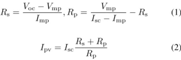
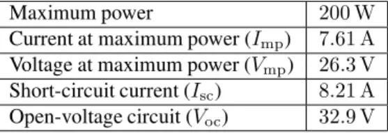
Arrays are composed of cascaded or paralleled photovoltaic cells and have characteristic curves similar (but not equal) to the curve of a single cell (in practice any association or array of cells is subject to partial shading, failure of cells and other external conditions that modify the behavior of the grouped devices). As noticed in Fig. 2, the photovoltaic array has a maximum power point (MPP). Ideally the array must operate at this point in order to deliver the maximum avail-able instantaneous power. Of course, in some applications full power may not be desired in certain situations, thus an-other operating point will be chosen. In grid-connected sys-tems the PV array is forced to operate at the MPP all time in order to extract and supply the grid with the maximum available instantaneous power. The parameters of the model of Fig. 1 can be obtained from Eqs. (1) and (2) with infor-mation found in datasheets supplied by PV array manufac-turers, which generally provide the open-circuit voltage of the array (Voc), the short-circuit current (Isc), the maximum-power voltage (Vmp) and the maximum-power current (Imp).
Rs=
Voc−Vmp
Imp
, Rp=
Vmp
Isc−Imp −
Rs (1)
Ipv=Isc
Rs+Rp
Rp
(2)
In many publications on photovoltaic systems the circuit of Fig. 3a is used as an array linear model. This circuit rep-resents the line that contains the segment 1 seen in Fig. 2. However, this circuit describes the behavior of the array only in the current-source region. Whenvpv > Vmp this model does not represent the array correctly. Fig. 3b shows another linear circuit that may be an array model. This circuit origi-nates the line that contains the segment 2 seen in Fig. 2 and describes the array in the voltage-source region of operation. This model is rare in the literature. If the array is modeled in the current-source region (line 1) the model error increases as
vpv> Vmp. Similarly, the error increases whenvpv < Vmp if the array is modeled as a voltage source (line 2). Both models are unable to correctly represent the array in its full operating range.
3
MODELING AND CONTROLLING THE
CONVERTER
+
-+
-ipv
Rp
Ipv
Rs
vpv
Voc
Figure 1: Equivalent circuit of the photovoltaic array.
ipv
Isc
Imp
Vmp Voc
vpv
current source
voltage source maximum power point
Figure 2: Simplified current vs. voltage curve of the photo-voltaic array.
section linear models for this photovoltaic-buck system and feedback systems with linear compensators are designed to control the input voltage of the converter.
3.1
Average voltage control with single
feedback loop
The first goal is to find the small-signal transfer function that describes the dynamic behavior of the input voltage of the converter of Fig. 4. The control variable is the duty cycled
of the transistor, which switches at the frequencyfs= 1/Ts. The transistor is ‘on’ during the intervaldTsand ‘off’ during
(1−d)Ts. Considering thatfsis sufficiently high, by inspec-tion of the circuit of Fig. 4 the state equainspec-tion of the inductor current may be written as in Eq. (3). The symbol<> repre-sents the average value of the variable (voltage or current) in a switching periodTs.
Ld < i >
dt =< v > d−Vo (3)
In order to obtain the small-signal AC model the average variables can be expressed as a sum of DC and AC compo-nents (Erickson and Maksimovic, 2001), as shown in Eq. (4). The symbol~ represents small AC perturbations and
capi-talized letters represent DC steady-state values. The minus signal in Eq. (4) means that a positive duty cycle increment causes an input voltage decrement.
< v >=V + ˜v, d=D−d, < i >˜ =I+ ˜i (4)
+
-+
-ipv
ipv
Ipv vpv Voc vpv
(a) (b)
Rs
Rs
Rp
Rp
Figure 3: Photovoltaic array linear equivalent circuits. (a) Current source. (b) Voltage source.
+ -v
+
-ipv
vpv Vo
PV array
i
C
L
Ts
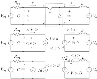
Figure 4: Buck converter with variable input and fixed output voltage fed by a photovoltaic (PV) array.
Eq. (5) is obtained from Eqs. (3) and (4). From Eq. (5), by neglecting the nonlinear productv˜d˜and applying the Laplace transform, the small-signal frequency-domain state equation seen in Eq. (6) is obtained.
Ld˜i
dt =V D+ ˜vD−Vd˜−v˜d˜−Vo (5)
sL˜i=−Vd˜+ ˜vD (6)
In the circuit of Fig. 4Veq andReqare the voltage and re-sistance of the equivalent Thévenin’s circuit of the models of Fig. 3. If the current source model (Fig. 3a) is used:
Veq = IpvRpandReq = Rp+Rs. If the voltage-source model (Fig. 3b) is used: Veq =VocandReq =Rs. Eq. (7) is obtained by inspecting the circuit of Fig. 4. Eq. (8) is ob-tained from Eqs. (7) and (4). From Eq. (8), by neglecting the nonlinear product˜id˜and applying the Laplace transform, the small-signal frequency-domain state equation seen in Eq. (9) is obtained.
Cd < v >
dt =
Veq−< v >
Req −
< i > d (7)
Veq−V −v˜
Req
+Id˜−˜iD−ID+ ˜id˜−Cd˜v
Figure 5: Bode plots ofGvd(s)using the current source
(con-tinuous line) and voltage source (dashed line) array models.
d v
Cvd Gvd
vref
Figure 6: Feedback control of the input voltage of the con-verter.
− v˜
Req
−sC˜v+Id˜−˜iD= 0 (9)
From Eqs. (6) and (9) the small-signal transfer function of Eq. (10) is obtained.
Gvd(s) =
˜
v(s) ˜
d(s) =
Req(V D+sLI)
s2R
eqLC+sL+D2Req
(10)
With a simple DC circuit analysis one finds the expressions of the steady-state valuesIandV of Eq. (11). These expres-sions may be substituted in Eq. (10).
I= Veq−V
ReqD
, V =Vo
D (11)
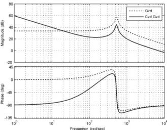
Fig. 5 compares the frequency responses ofGvd(s)when the
PV array models of Figs. 3a and 3b are used. The Bode plots of Fig. 5 were obtained with the transfer functions of the PV-buck system with the parameters and characteristics shown in Tables 1 and 2. When the current source model (Fig. 3a) is used,Gvd(s)presents a resonance with an abrupt phase shift
near 500 rad/s. When the voltage source model (Fig. 3b) is
Table 1: KC200GT solar panel - nominal characteristics. Maximum power 200 W
Current at maximum power (Imp) 7.61 A
Voltage at maximum power (Vmp) 26.3 V
Short-circuit current (Isc) 8.21 A
Open-voltage circuit (Voc) 32.9 V
Table 2: Characteristics of the simulated converter.
L 2mH
C 450µF
Vo 12 V
D 0.5
fs 10 kHz
used, Gvd(s)presents a low-pass response without any
im-portant characteristics.
Although neither of the models of Fig. 3 represents the PV array in its full operating range, the circuit of Fig. 3a is a suitable array linear model for the purpose of modeling the PV-buck system. By comparing the Bode plots of Fig. 5 it is possible to conclude that a feedback control system designed for the current source region of the photovoltaic array will automatically fit for the operation in the voltage-source re-gion. In other words, the control system is designed for the worst case.
The system response with the voltage-source model offers no design difficulties because it is similar to a low-pass filter. The response with the current-source model is more com-plicated due to the presence of a resonance and an abrupt phase shift (Villalva and Ruppert F., 2008). Fig. 6 shows the feedback system employed in the control of the input volt-agev of the converter. The compensatorCvd(s)may be a
proportional-integral one designed with conventional tech-niques of control systems (Villalva and Ruppert F., 2007). Fig. 7 shows the frequency response ofGvd(s)compensated
withCvd(s) = 0.2 + 20/s, which results a crossover
fre-quency of approximately 34000 rad/s and a margin phase of
86◦. Low steady-state error and a fast control response may
be ensured with a correct compensator design.
3.2
Average voltage control with inner
av-erage current control loop
The second control strategy proposed here employs two small-signal transfer functions,Gvd(s)andGid(s). The
Figure 7: Bode plots ofGvd(s)(dashed line) and of the
com-pensated transfer functionCvd(s)Gvd(s)(continuous line).
Gid(s) =
˜i(s) ˜
d(s) =
−V(1 +sReqC) +ReqDI
s2L R
eqC+sL+ReqD2
(12)
Fig. 8 shows the frequency response ofGid(s) and Fig. 9
shows its root locus. The transfer function was obtained for the system with the characteristics shown in Tables 1 and 2, considering the current-source PV array model. This system has a right-half-plane zero and its root locus is mostly on the right half-plane, which brings some difficulty for the design of the feedback control loop. The Bode plot of Fig. 8 shows that near the crossover frequency there is a phase shift of al-most180◦. Such a marginally stable system requires special
attention.
Fig. 10 shows the current control loop with the compensator
Cid(s). This compensator may be a simple
proportional-integral one, but the proportional gain must be carefully cho-sen in order to set a crossover frequency with a good phase margin, keeping all system poles on the left half plane. Be-cause the root locus is mostly on the right side of thesplane, there are strong constraints in the design of the compensator
Cid(s).
A compensator with a low proportional gain, an integrator at the origin and a zero placed at a low frequency makes this system stable. The system poles fall on the outside of the left half plane, making the system unstable, if the closed-loop crossover frequency is set above the resonance frequency of
Gid(s). The only option to stabilize this system is keeping
the magnitude at the resonance frequency bellow 0 dB. The stabilization of the current loop results a very low current control bandwidth. Fig. 8 shows the Bode plot of Gid(s)
compensated withCid(s) = 1.3·10−4(s+ 836.1)/s.
Figure 8: Bode plots ofGid(s)(dashed line) and of the
com-pensated systemCid(s)Gid(s)(continuous line).
Figure 9: Root locus ofGid(s).
A low current-control bandwidth, however, does not mean the system will not work properly. Fig. 10 shows that an external voltage-control loop may be employed. The combi-nation of the inner current loop and the outer voltage loop re-sults a closed-loop system whose transient voltage response may be fast or low according to the design of the voltage compensatorCvi(s). The voltage control may be fast
al-though the minor current loop is inherently slow. The goal now is to design the voltage compensatorCvi(s)used in the
scheme of Fig. 10. Fig. 11 shows the frequency response ofFi(s)Gvd(s) whereFi(s) = Cid/(1 +CidGid). The
compensatorCvi(s)must stabilize the outer voltage loop. A
d
v
i
Cvi Cid
vref iref
Gid
Gvd
Figure 10: Control system of the input voltage with inner current loop.
Figure 11: Frequency responses of Fi(s)Gvd(s) and of Cvi(s)Fi(s)Gvd(s).
3.3
Voltage control with analog peak
cur-rent control
In this control strategy the inductor current is directly con-trolled with an analog peak current controller. The control of the input voltage is achieved with an external control loop that provides the current reference for the current controller. Fig. 12 shows the simplified scheme of the analog peak cur-rent controller. A square-wave oscillator sets the flip-flop and turns ‘on’ the transistor at the beginning of the switching pe-riodTs. The inductor currentiis compared with the current referenceiref. Wheni > iref the flip-flop is reset and the transistor is ‘off’ until the beginning of the next cycle.
Fig. 13 illustrates a typical inductor current waveform ob-tained with this control scheme. The transistor duty cycle is automatically adjusted in order to keep the inductor current near the desired reference current. When the duty cycle is greater than 0.5 this control scheme tends to become unsta-ble (Erickson and Maksimovic, 2001; Pressman, 1997).
The stabilizing ramp signal seen in the scheme of Fig. 12 is necessary for the proper operation of the converter. The
sta-RAMP GENERATOR
CLOCK PULSESGATING FOR THE TRANSISTOR
ANALOG COMPARATOR MEASURED
CURRENT
REFERENCE CURRENT
fs fs
i
iref
Figure 12: Analog inductor peak current controller.
∆i
∆T i iref
Figure 13: Waveform of the inductor current with peak cur-rent control.
bilization with the ramp signal increases the control error, as the peak of the controlled current gets farther from the ref-erence (Erickson and Maksimovic, 2001; Pressman, 1997). However, if this control scheme is employed as the inner part of a control system with an external voltage-control loop the current error has no influence because the current reference is adjusted by the voltage compensator, thus canceling the effect of the current error.
Fig. 14 shows a strategy for controlling the input voltage of the buck converter with the peak current controller of Fig. 12. The input voltagevis fed back and compared with the volt-age referencevref. The current referenceiref is determined by the voltage compensatorCv(s).
The design of theCv(s)compensator requires a
mathemat-ical model that describes the behavior of the converter op-erating with this analog current-control scheme. In order to obtain a converter model one can assume that the control of the inductor current is instantaneous. If the current has a small ripple∆iand a small error due to the stabilizing ramp,
the average inductor current< i > approximately follows the referenceiref. These assumptions are generally valid in a well-dimensioned converter with low current and voltage ripples. When the referenceirefis perturbed the inductor av-erage current< i >is instantaneously adjusted except by the time∆T it takes for the inductor current to grow till its peak
reaches the value of the reference signal at the(+)terminal of the comparator – this is illustrated in Fig. 13.
cur-CURRENT
CONTROLLER CONVERTER
Cv
Gvi
iref
vref i v
Figure 14: Voltage control employing inner system with peak current control.
rent rises linearly during the interval∆T, beginning when
a reference step occurs. During this interval (∆T >> Ts)
the transistor remains ‘on’ and the duty cycle isd = 1. In other words, the converter is out of control during the inter-val∆T. The transistor is simply turned ‘on’ and so it remains
until the flip-flop receives a reset signal. This behavior is ex-tremely nonlinear and difficult to model, since the duration of∆T depends on several variables such as the inductance L, the size of the reference step, and the instantaneous input voltage.
Considering that the dynamics of the current controller de-pends mainly on the duration of ∆T, which is generally
small, this delay may be neglected and the peak current control scheme may be considered practically instantaneous. This simplifies the task of modeling the PV-buck system and permits to obtain the equivalent circuit of Fig. 15. Current is drained from the photovoltaic array and from the capacitor by a controlled current source. Provided that the analog cur-rent controller of Fig. 12 is capable of maintaining the induc-tor current regulated, the current flowing through the current source of Fig. 15 may be expressed as Eq. (13), whereD is the steady-state duty cycle of the transistor.
< ie >=< i > D≈irefD (13)
With Eq. (13), using the definitions of Eq. (14), the transfer functionGvi(s)of Eq. (15) is obtained.
< v >=V + ˜v, < i >=I+ ˜i, < ie>=Ie+ ˜ie, iref =Iref+ ˜iref
(14)
Gvi(s) =
˜
v
˜iref =−
Veq−V
I(1 +sReqC)
(15)
Fig. 16 shows the frequency response of the transfer function Gvi(s) and of the compensated transfer function Cv(s)Gvi(s). Gvi(s)was obtained with the voltage source
PV array model. Because the time response of the open-loop system depends on the initial capacitor charge, which
C
...
...
Veq
Req
< iC>
< ie>
Figure 15: Equivalent circuit of the photovoltaic-buck sys-tem with peak current control.
Figure 16: Frequency response ofGvi(s)(dashed line) and
of the compensated transfer functionCv(s)Gvi(s)
(continu-ous line).
depends on the open-circuit voltage of the PV array, the voltage-source model is more appropriate for the analysis of this system. The compensatorCv(s) may be a simple
proportional-integral one. This system is not critical and the compensator design is straightforward. This example uses
Cv(s) = (10s+ 5000)/s.
4
SIMULATION RESULTS
Figure 17: Step response ofGvd(s)and input voltage of the
switching buck converter with duty-cycle control.
Figure 18: Step response ofGid(s)and inductor current of
the switching buck converter with duty-cycle control.
of the simulated open-loop converter.
Open-loop converter
Fig. 17 shows the open-loop step response of the transfer functionGvd(s)superimposed with the response of the
sim-ulated switching converter. This transfer function almost ex-actly represents the behavior of the switching converter re-garding the duty cycle of the transistor and the capacitor volt-age. Fig. 18 shows the open-loop step response of the trans-fer functionGid(s)superimposed with the response of the
simulated switching converter. This transfer function repre-sents the behavior of the switching converter regarding the duty cycle of the transistor and the inductor current.
The frequency responses of the converter were obtained by simulation in order to verify that the developed transfer func-tions exactly describe the behavior of the converter. Bode plots of the open-loop transfer functionsGvd(s)andGid(s)
have been presented in Figs. 5 and 8, in Section 3, and now will be compared to frequency responses obtained by simu-lation.
The equivalent AC model of the PV-buck system is ob-tained in the Appendix. Fig. 30c shows the AC/DC model used in PSpice to obtain the converter frequency responses of Figs. 19 and 20. Because PSpice is unable to achieve frequency analysis of systems containing nonlinear
switch-Figure 19: Frequency responses (superimposed) ofGvd(s)
and of the AC model of Fig. 30.
ing elements, an equivalent AC model without the nonlinear switches (transistor and diode) is necessary.
Figs. 19 and 20 show that the frequency responses of the sim-ulated converter (equivalent AC model) exactly coincide with the responses of the theoretical transfer functions presented in Section 3. Please notice that in Figs. 19 and 20 the fre-quencies are expressed in Hz, while in Section 3 the frequen-cies are in rad/s.
Average voltage control
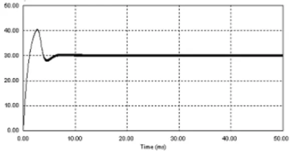
Fig. 21 shows the result of the simulated switching converter with the feedback system of Fig. 6, Section 3.1. The input voltagevreaches the reference with zero steady-state error.
Average voltage and current control
Fig. 22 shows the result of the converter controlled with the double feedback loop scheme of Fig. 10, Section 3.2. The input voltagevof the converter reaches the reference voltage with zero steady-state error. Fig. 23 shows the behavior of the inductor current, which is also controlled in this case.
Average voltage and peak current control
Fig. 24 shows the open-loop step response of the transfer functionGvi(s)superimposed with the response of the
sim-ulated switching converter. This transfer function approx-imately represents the system behavior for small and even large voltage oscillations near the nominal operating point.
cir-Figure 20: Frequency responses (superimposed) ofGid(s)
and of the AC model of Fig. 30.
Figure 21: Input voltage (vref= 30 V) of the buck converter with the control system designed in Section 3.1 (single volt-age loop).
cuit model of Fig. 15. The error between the responses of the transfer function and of the real system is mainly due to the approximation< i > D ≈ iref. This system has a
nonzero initial condition, since the initial capacitor charge does not depend on the existence of current flow through the controlled current source of Fig. 15. The DC value of the transfer functionGvi(s)may not coincide with the
steady-state voltageV.
In order to verify the validity of the converter transfer func-tion developed in the previous secfunc-tion the Bode plot of the theoretical transfer function Gvi(s) (Fig. 16) is compared
with the frequency response of the equivalent circuit. Fig. 25 shows the frequency response of the model circuit of Fig. 15 superimposed with the Bode plot ofGvi(s). Fig. 26 shows
the result of the closed-loop photovoltaic-buck system oper-ating with the current controller of Fig. 12 and the control system of Fig. 14, with the compensator designed in Section 3.3.
Figure 22: Input voltage (vref = 30 V) of the buck converter with the control system designed in Section 3.2 (voltage loop combined with inner current loop).
Figure 23: Inductor current of the buck converter obtained with the inner control loop designed in Section 3.2.
5
EXPERIMENTAL RESULTS
An experimental buck converter was built in order to validate the transfer function and the compensator developed in Sec-tion 3.1. Fig. 27 shows a picture of the experimental setup. The PV array with the parameters of Table 1 was simulated with the Agilent E4350B solar array simulator. The control system was implemented with a PIC18F452 microcontroller. The PWM frequency was set at 20 kHz and the digital con-trol loop was implemented with a sampling rate of 5 kHz. The characteristics of the converter are summarized in Table 3.
time (ms)
Figure 24: Responses ofGvi(s), of the open-loop buck
Figure 25: Frequency responses (superimposed) ofGvi(s),
and of the equivalent circuit of Fig. 15.
Figure 26: Input voltage (vref= 30 V) of the buck converter with the control system designed in Section 3.3 (voltage loop with inner peak current controller).
Fig. 28 shows the closed-loop input voltage of the experi-mental converter. The proportional and integral compensator has the following parameters: ki = 2, kp = 500. The feedback gain of the input voltage is1/62. For comparison, Fig. 29 shows the input voltage obtained with the simulated converter and its transfer function. The converter response differs of the transfer function response because the initial conditions are different. It is difficult to obtain in practice the zero-voltage condition for the input voltage because the capacitor is charged with the open-circuit voltage of the PV array when the converter is off.
Table 3: Characteristics of the experimental buck converter.
C 1000µF
L 5 mH
fs(switching) 20 kHz
Tsample(digital control) 200µs
Figure 27: Experimental buck converter.
Figure 28: Closed-loop input voltage of the experimental buck converter (vref = 20 V).
SIMULATED CONVERTER
TRANSFER FUNCTION
time (s)
+ -+ -2 1 4 3 + -+ -Veq Veq Veq Req Req Req Vo Vo Vo i1
< i1>
< i > < i >
i v L L L v2
< v2>
< v >
Vd˜
Id˜
< i > d
< v > d
< i > D
< V > D C
C
C
Figure 30: (a) Original PV-buck system with switching ele-ments. (b) Nonlinear circuit with dependent sources replac-ing the switchreplac-ing elements. (c) Equivalent linear circuit with dependent sources.
6
CONCLUSIONS
Section 2 has demonstrated why the current-source PV array model is more convenient than the voltage-source one for the purpose of modeling this input-controlled PV system. Al-though neither of the models represents the array in its full operating range, the current-source model may be adopted and considered as a suitable representation of the PV array.
Section 3 has presented the development of converter transfer functions for the input voltage control of the buck converter operating with duty-cycle control (voltage mode) and with inductor peak current control (current-programmed mode). The transfer functions reveal important dynamic characteris-tics of the input-controlled buck converter when it is fed by a PV array. With these transfer functions it is possible to de-sign compensators and feedback controllers for the control of the input voltage of the buck converter.
The modeling and control approaches developed in this pa-per are intended for the control of the input voltage of the buck converter. Many authors diverge about the advantages and disadvantages of controlling the input voltage (i.e. di-rectly controlling the PV array output voltage according to a voltage reference) or the inductor current (i.e. indirectly con-trolling the PV output through the regulation of the buck cur-rent). This depends mainly on the kind of MPPT algorithm employed. Many works deal with the control of the output voltage of the PV array, so the input voltage of the converter
is controlled in order to adjust the PV voltage. Some au-thors have studied control strategies that achieve the MPPT through the control of the buck inductor current (Enslin and Snyman, 1992).
Sections 3.1 and 3.2 have focused on the control of the aver-age input voltaver-age and inductor current of the converter. The model developed in Section 3.3 corresponds to the control of the converter with inductor peak current control.
Section 4 has presented results obtained with simulated switching converters. These results show that the proposed models and transfer functions correctly describe the dynamic behavior of the studied photovoltaic-buck system. The open-loop transfer functionsGvd(s), Gid(s), and Gvi(s)
accu-rately describe the behavior of the converter. In order to certify that the results were correct the frequency and time responses of the open-loop transfer functions have been com-pared to the responses of simulated converters. The re-sponses have almost exactly coincided both in the time and in the frequency domains. The results presented in the previ-ous sections show that the compensators designed in Section 3 can be employed to fast and accurately control the input voltage of the DC-DC buck converter fed by a PV array.
APPENDIX: EQUIVALENT AC MODEL
< i > d= (I+ ˜i)(D−d˜) =
=ID+ ˜iD−˜id˜−Id˜≈D(I+ ˜i)−Id˜ (16)
< v > d= (V + ˜v)(D−d˜) =
=V D+ ˜vD−˜vd˜−Vd˜≈D(V + ˜v)−Vd˜ (17)
The linear circuit of Fig. 30c represents with good accuracy the original switching circuit of Fig. 30a, both for DC and AC signals. If the DC sourcesVeqandVo of Fig. 30c are short-circuited, the remainder circuit is the desired equivalent AC model of the PV-buck converter ready to be used in the PSpice AC SWEEP analysis.
REFERENCES
Blaabjerg, F. (2006). Power converters and control of renew-able energy systems,Proc. 37th IEEE PESC.
Calais, M., Myrzik, J., Spooner, T. and Agelidis, V. (2002). Inverters for single-phase grid connected photovoltaic systems - an overview, Proc. 33rd IEEE PESC, v. 4, pp. 1995–2000.
Cho, Y.-J. and Cho, B. (1997). A digital controlled so-lar array regulator employing the charge control,Proc. 32nd IECEC, v. 4, pp. 2222–2227.
Enslin, J. and Snyman, D. (1992). Simplified feed-forward control of the maximum power point in PV instal-lations, Proc. International Conference on Industrial Electronics, Control, Instrumentation, and Automation, pp. 548–553.
Erickson, R. W. and Maksimovic, D. (2001). Fundamentals of Power Electronics, Kluwer Academic Publishers.
Kislovski, A. S. (1990). Dynamic behavior of a constant-frequency buck converter power cell in a photovoltaic battery charger with a maximum power tracker,Proc. 5th IEEE APEC.
Kjaer, S., Pedersen, J. and Blaabjerg, F. (2002). Power inverter topologies for photovoltaic modules-a review,
Proc. 37th IAS Industry Applications Conf., v. 2, pp. 782–788.
Koutroulis, E., Kalaitzakis, K. and Voulgaris, N. (2001). Development of a microcontroller-based, photovoltaic maximum power point tracking control system, IEEE Trans. on Power Electronics 16(1): 46–54.
Lai, J., Krein, P. and Levran, A. (2008). Power electron-ics for alternative energy,Professional Education Sem-inars Workbook. APEC.
Machado, G. and Pomilio, J. A. (2004). Controle de um sistema de geração distribuída alimentado por célula a combustível composto por conversor boost e inversor,
Proc. XV CBA.
Martins, D. C. (2005). Novas perspectivas da energia solar fotovoltaica no brasil,Proc. VIII COBEP.
Martins, D. C., Weber, C. L., Gonçalves, O. H. and Andrade, A. S. (2004). PV solar energy system distribution using MPP technique,Proc. VI INDUSCON.
Martins, D., Weber, C. and Demonti, R. (2002). Photovoltaic power processing with high efficiency using maximum power ratio technique,Proc. 28th IEEE IECON, v. 2, pp. 1079–1082.
Mocci, F. and Tosi, M. (1989). Comparison of power con-verter technologies in photovoltaic applications,Proc. Mediterranean Electrotechnical Conf., pp. 11–15.
Pressman, A. I. (1997). Switching Power Supply Design, McGraw-Hill.
Salas, V., Manzanas, M., Lazaro, A., Barrado, A. and Olias, E. (2002a). Analysis of control strategies for solar reg-ulators,Proc. IEEE ISIE, v. 3, pp. 936–941.
Salas, V., Manzanas, M., Lazaro, A., Barrado, A. and Olias, E. (2002b). The control strategies for photovoltaic reg-ulators applied to stand-alone systems,Proc. 28th IEEE IECON, v. 4, pp. 3274–3279.
Villalva, M. G. and Ruppert F., E. (2007). Buck converter with variable input voltage for photovoltaic applica-tions,Proc. IX COBEP.
Villalva, M. G. and Ruppert F., E. (2008). Input-controlled buck converter for photovoltaic applications: modeling and design,Proc. 4th IET PEMD, pp. 505–509.